National Semiconductor LM7705 User manual

LM7705
LM7705 Low Noise Negative Bias Generator
Literature Number: SNVS420A

LM7705
June 10, 2009
Low Noise Negative Bias Generator
General Description
The LM7705 is a switched capacitor voltage inverter with a
low noise, −0.23V fixed negative voltage regulator. This de-
vice is designed to be used with low voltage amplifiers to
enable the amplifiers output to swing to zero volts. The −0.23
volts is used to supply the negative supply pin of an amplifier
while maintaining less then 5.5 volts across the amplifier. Rail-
to-Rail output amplifiers cannot output zero volts when oper-
ating from a single supply voltage and can result in error
accumulation due to amplifier output saturation voltage being
amplified by following gain stages. A small negative supply
voltage will prevent the amplifiers output from saturating at
zero volts and will help maintain an accurate zero through a
signal processing chain. Additionally, when an amplifier is
used to drive an ADC’s input, it can output a zero voltage sig-
nal and the full input range of an ADC can be used. The
LM7705 has a shutdown pin to minimize standby power con-
sumption
Features
■Regulated output voltage −0.232V
■Output voltage tolerance 5%
■Output voltage ripple 4 mVPP
■Max output current 26 mA
■Supply voltage 3V to 5.25V
■Conversion efficiency up to 98%
■Quiescent current 78 µA
■Shutdown current 20 nA
■Turn on time 500 µs
■Operating temperature range −40°C to 125°C
■8-Pin MSOP Package
Applications
■True zero amplifier output
■Portable instrumentation
■Low voltage split power supplies
Typical Application
20173001
© 2009 National Semiconductor Corporation 201730 www.national.com
LM7705 Low Noise Negative Bias Generator

Absolute Maximum Ratings (Note 1)
If Military/Aerospace specified devices are required,
please contact the National Semiconductor Sales Office/
Distributors for availability and specifications.
Supply Voltage
VDD - VSS +5.75V
SD VDD+0.3V, VSS-0.3V
ESD Tolerance (Note 2)
Human Body Model
For input pins only 2000V
For all other pins 2000V
Machine Model 200V
Charge Device Model 750V
Storage Temp. Range −65°C to 150°C
Junction Temperature (Note 7) 150°C max
Mounting Temperature
Infrared or Convection (20 sec) 260°C
Operating Ratings
Supply Voltage ( VDD to GND) 3V to 5.25V
Supply Voltage ( VDD wrt VOUT)3.23V to 5.48V
Temperature Range −40°C to 125°C
Thermal Resistance (θJA )
8-Pin MSOP 253°C/W
3.3V Electrical Characteristics
Unless otherwise specified, all limits are guaranteed for TA= 25°C, VDD = 3.3V, VSS = 0V, SD = 0V, CFLY= 5 µF, CRES = 22 µF,
COUT = 22 µF. Boldface limits apply at temperature extremes (Note 5).
Symbol Parameter Conditions Min
(Note 6)
Typical
(Note 7)
Max
(Note 6)
Units
VOUT Output Voltage IOUT = 0 mA −0.242
−0.251
−0.232 −0.219
−0.209 V
IOUT = −20 mA −0.242
−0.251
−0.226 −0.219
−0.209
VROutput Voltage Ripple IOUT = −20 mA 4 mVPP
ISSupply Current No Load 50 78 100
150 μA
ISD Shutdown Supply Current SD = VDD 20 nA
ηPOWER Current Conversion Efficiency −5 mA ≤IOUT ≤−20 mA 98 %
ηPOWER Current Conversion Efficiency IOUT = −5 mA 98 %
tON Turn On Time IOUT = −5 mA 500 μs
t OFF Turn Off Time IOUT = −5 mA 700 μs
tOFF CP Turn Off Time Charge Pump IOUT = −5 mA 11 μs
ZOUT Output Impedance −1 mA ≤IOUT ≤−20 mA 0.23 0.8
1.3 Ω
IO_MAX Maximum Output Current VOUT < −200 mV -26 mA
fOSC Oscillator Frequency 92 kHz
VIL Shutdown Input Low 1.6
1.25 V
VIH Shutdown Input High 1.85
2.15
V
ICShutdown Pin Input Current SD = VDD 50 pA
Load Regulation 0 mA ≤IOUT ≤−20 mA 0.12 0.6
0.85 %/mA
Line Regulation 3V ≤VDD ≤5.25V (No Load) -0.2 0.29 0.7
1.1 %/V
www.national.com 2
LM7705

5.0V Electrical Characteristics Unless otherwise specified, all limits are guaranteed for TA= 25°C, VDD =
5.0V, VSS = 0V, SD = 0V, CFLY = 5 µF, CRES = 22 µF, COUT = 22 µF. Boldfacelimits apply at temperature extremes (Note 5).
Symbol Parameter Conditions Min
(Note 6)
Typical
(Note 7)
Max
(Note 6)
Units
VOUT Output Voltage IOUT = 0 mA −0.242
−0.251
−0.233 −0.219
−0.209 V
IOUT = −20 mA −0.242
−0.251
−0.226 −0.219
−0.209
VROutput Voltage Ripple IOUT = −20 mA 4 mVPP
ISSupply Current No Load 60 103 135
240 μA
ISD Shutdown Supply Current SD = VDD 20 nA
ηPOWER Current Conversion Efficiency −5 mA ≤IOUT ≤−20 mA 98 %
ηPOWER Current Conversion Efficiency IOUT = −5 mA 98 %
tON Turn On Time IOUT = −5 mA 200 μs
t OFF Turn Off Time IOUT = −5 mA 700 μs
tOFF CP Turn Off Time Charge Pump IOUT = −5 mA 11 μs
ZOUT Output Impedance −1 mA ≤IOUT ≤−20 mA 0.26 0.8
1.3 Ω
IO_MAX Maximum Output Current VOUT < − 200 mV −35 mA
fOSC Oscillator Frequency 91 kHz
VIL Shutdown Input Low 2.55
1.95 V
VIH Shutdown Input High 2.8
3.25
V
ICShutdown Pin Input Current SD = VDD 50 pA
Load Regulation 0 mA ≤IOUT ≤−20 mA 0.14 0.6
0.85 %/mA
Line Regulation 3V ≤VDD ≤5.25V (No Load) −0.2 0.29 0.7
1.1 %/V
Note 1: Absolute Maximum Ratings indicate limits beyond which damage to the device may occur. Operating Ratings indicate conditions for which the device is
intended to be functional, but specific performance is not guaranteed. For guaranteed specifications and test conditions, see the Electrical Characteristics.
Note 2: Human Body Model, applicable std. MIL-STD-883, Method 3015.7. Machine model, applicable std JESD22–A115–A (ESSD MM srd of JEDEC). Field
induced Charge-Device Model, applicable std. JESD22–C101–C. (ESD FICDM std of JEDEC).
Note 3: The maximum power dissipation is a function of TJ(MAX), θJA, and TA. The maximum allowable power dissipation at any ambient temperature is
PD= (TJ(MAX) - TA)/ θJA. All numbers apply for packages soldered directly onto a PC board.
Note 4: Electrical Table values apply only for factory testing conditions at the temperature indicated. Factory testing conditions result in very limited self-heating
of the device such that TJ= TA. No guarantee of parametric performance is indicated in the electrical tables under conditions of internal self-heating where
TJ> TA.
Note 5: Boldface limits apply to temperature range of −40°C to 125°C
Note 6: All limits are guaranteed by testing or statistical analysis.
Note 7: Typical values represent the most likely parametric norm as determined at the time of characterization. Actual typical values may vary over time and will
also depend on the application and configuration. The typical values are not tested and are not guaranteed on shipped production material.
3 www.national.com
LM7705

Connection Diagram
8-Pin MSOP
20173002
Top View
Pin Descriptions
Pin Number Symbol Description
1 CF+ CFLY Positive Capacitor Connection
2 VSS Power Ground
3 SD Shutdown Pin
If SD pin is LOW, device is ON
If SD pin is HIGH, device is OFF
4 VDD Positive Supply Voltage
5 VSS Power Ground
6 VOUT Output Voltage
7 CRES Reserve Capacitor Connection
8 CF- CFLY Negative Capacitor Connection
Ordering Information
Package Part Number Package Marking Transport Media NSC Drawing
8-Pin MSOP
LM7705MM
F26A
1k Units Tape and Reel
MUA08ALM7705MME 250 Units Tape and Reel
LM7705MMX 3.5k Units Tape and Reel
Block Diagram
20173003
LM7705
www.national.com 4
LM7705

Typical Performance Characteristics VDD = 3.3V and TA= 25°C unless otherwise noted.
Output Voltage vs. Supply Voltage
20173010
Supply Current vs. Supply Voltage
20173011
Output Voltage vs. Output Current
20173012
Output Voltage vs. Output Current
20173013
Output Voltage Ripple vs. Temperature
20173014
Output Voltage Ripple vs. Temperature
20173015
5 www.national.com
LM7705

Supply Current vs. Output Current
20173016
Supply Current vs. Output Current
20173017
Current Conversion Efficiency vs. Output Current
20173018
Current Conversion Efficiency vs. Output Current
20173019
Turn On Time
20173020
Turn On Time
20173021
www.national.com 6
LM7705

Load Regulation vs. Temperature
20173022
Load Regulation vs. Temperature
20173023
Transient Response
20173024
Transient Response
20173025
Transient Response
20173029
Transient Response
20173030
7 www.national.com
LM7705

Output voltage vs. shutdown Voltage
20173026
Supply Current vs. Shutdown Voltage
20173027
Oscillator Frequency vs. Temperature
20173028
www.national.com 8
LM7705

Application Information
This applications section will give a description of the func-
tionality of the LM7705. The LM7705 is a switched capacitor
voltage inverter with a low noise, −0.23V fixed negative bias
output. The part will operate over a supply voltage range of 3
to 5.25 Volt. Applying a logical low level to the SD input will
activate the part, and generate a fixed −0.23V output voltage.
The part can be disabled; the output is switched to ground
level, by applying a logical high level to the SD input of the
part.
FUNCTIONAL DESCRIPTION
The LM7705, low noise negative bias generator, can be used
for many applications requiring a fixed negative voltage. A key
application for the LM7705 is an amplifier with a true zero
output voltage using the original parts, while not exceeding
the maximum supply voltage ratings of the amplifier.
The voltage inversion in the LM7705 is achieved using a
switched capacitor technique with two external capacitors
(CFLY and CRES). An internal oscillator and a switching net-
work transfers charge between the two storage capacitors.
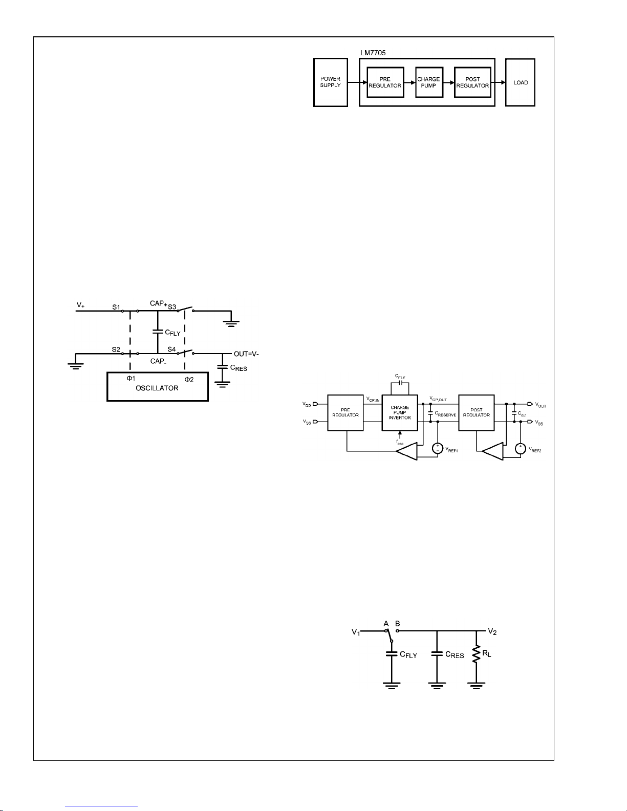
This switched capacitor technique is given in Figure 1.
20173034
FIGURE 1. Voltage Inverter
The internal oscillator generates two anti-phase clock signals.
Clock 1 controls switches S1 and S2. Clock 2 controls switch-
es S3 and S4. When Switches S1 and S2 are closed, capac-
itor CFLY is charged to V+. When switches S3 and S4 are
closed (S1 and S2 are open) charge from CFLY is transferred
to CRES and the output voltage OUT is equal to -V+.
Due to the switched capacitor technique a small ripple will be
present at the output voltage, with a frequency of the oscilla-
tor. The magnitude of this ripple will increase for increasing
output currents. The magnitude of the ripple can be influenced
by changing the values of the used capacitors.
In the next section a more detailed technical description of the
LM7705 will be given.
TECHNICAL DESCRIPTION
As indicated in the functional description section, the main
function of the LM7705 is to supply a stabilized negative bias
voltage to a load, using only a positive supply voltage. A gen-
eral block diagram for this charge pump inverter is given in
Figure 2. The external power supply and load are added in
this diagram as well.
20173031
FIGURE 2. LM7705 Architecture
The architecture given in Figure 2 shows that the LM7705
contains 3 functional blocks:
•Pre-regulator
•Charge pump inverter
•Post-regulator
The output voltage is stabilized by:
•Controlling the power supplied from the power supply to
the charge pump input by the pre-regulator
•The power supplied from the charge pump output to the
load by the post-regulator.
A more detailed block diagram of the negative bias generator
is given in Figure 3. The control of the pre-regulator is based
on measuring the output voltage of the charge pump. The goal
of the post-regulator is to provide an accurate controlled neg-
ative voltage at the output, and acts as a low pass filter to
attenuate the output voltage ripple. The voltage ripple is a re-
sult of the switching behavior of the charge pump and is
dependent of the output current and the values of the used
capacitors.
20173003
FIGURE 3. Charge Pump Inverter with Input/Output
Control
In the next section a simple equation will be derived, that
shows the relation between the ripple of the output current,
the frequency of the internal clock generator and the value of
the capacitor placed at the output of the LM7705.
Charge Pump Theory
This section uses a simplified but realistic equivalent circuit
that represents the basic function of the charge pump. The
schematic is given in Figure 4.
20173033
FIGURE 4. Charge Pump
9 www.national.com
LM7705

When the switch is in position A, capacitor CFLY will charge to
voltage V1. The total charge on capacitor CFLY is Q1= CFLY x
V 1. The switch then moves to position B, discharging CFLY to
voltage V2. After this discharge, the charge on CFLY will be
Q2= CFLY x V2. Note that the charge has been transferred
from the source V1to the output V2. The amount of charge
transferred is:
(1)
When the switch changes between A and B at a frequency f,
the charge transfer per unit time, or current is:
(2)
The switched capacitor network can be replaced by an equiv-
alent resistor, as indicated in Figure 5.
20173032
FIGURE 5. Switched Capacitor Equivalent Circuit
The value of this resistor is dependent on both the capacitor
value and the switching frequency as given in Equation 3
(3)
The value for REQ can be calculated from Equation 3 and is
given in Equation 4
(4)
Equation 4 show that the value for the resistance at an in-
creased internal switching frequency, allows a lower value for
the used capacitor.
Key Specification
The key specifications for the LM7705 are given in the fol-
lowing overview:
Supply Voltage The LM7705 will operate over a supply
voltage range of 3V to 5.25V, and meet
the specifications given in the Electrical
Table. Supply voltage lower than 3.3 Volt
will decrease performance (The output
voltage will shift towards zero, and the
current sink capabilities will decrease) A
voltage higher than 5.25V will exceed the
Abs Max ratings and therefore damage
the part.
Output Voltage/
Line Regulation
The fixed and regulated output voltage of
−0.23 V has tight limits, as indicated in the
Electrical Characteristics table, to guar-
antee a stable voltage level. The usage of
the pre- and post regulator in combination
with the charge pump inverter ensures
good line regulation of 0.29%/V
Output current/
Load regulation
The LM7705 can sink currents > 26 mA,
causing an output voltage shift to −200
mV. A specified load-regulation of 0.14%
mA/V ensures a minor voltage deviation
for load current up to 20 mA.
Quiescent
current
The LM7705 consumes a quiescent
current less than 100 µA. Sinking a load
current, will result in a current conversion
efficiency better than 90%, even for load
currents of 1 mA, increasing to 98% for a
current of 5mA.
In the next section a general amplifier application requiring a
true-zero output, will be discussed, showing an increased
performance using the LM7705.
GENERAL AMPLIFIER APPLICATION
This section will discuss a general DC coupled amplifier ap-
plication. First, one of the limitations of a DC coupled amplifier
is discussed. This is illustrated with two application examples.
A solution is a given for solving this limitation by using the
LM7705.
Due to the architecture of the output stage of general ampli-
fiers, the output transistors will saturate. As a result, the output
of a general purpose op amp can only swing to a few 100 mV
of the supply rails. Amplifiers using CMOS technology do
have a lower output saturation voltage. This is illustrated in
Figure 6. E.g. National Semiconductors LM7332 can swing to
200 mV to the negative rail, for a 10 kΩload, over all tem-
peratures.
www.national.com 10
LM7705

20173040
FIGURE 6. Limitation of the Output of an Amplifier
The introduction of operational amplifiers with output Rail-to-
rail drive capabilities is a strong improvement and the (output)
performance of op amps is for many applications no longer a
limiting factor. For example, National Semiconductors
LMP7701 (a typical rail-to-rail op amp), has an output drive
capability of only 50 mV over all temperatures for a 10 kΩload
resistance. This is close to the lower supply voltage rail.
However, for true zero output applications with a single sup-
ply, the saturation voltage of the output stage is still a limiting
factor. This limitation has a negative impact on the function-
ality of true zero output applications. This is illustrated in
Figure 7.
20173041
FIGURE 7. Output Limitation for Single Supply True Zero
Output Aapplication
In the following section, two applications will be discussed,
showing the limitations of the output stage of an op amp in a
single supply configuration.
•A single stage true zero amplifier, with a 12 bit ADC back
end.
•A dual stage true zero amplifier, with a 12 bit ADC back
end.
One-stage, Single Supply True Zero Amplifier
This application shows a sensor with a DC output signal, am-
plified by a single supply op amp. The output voltage of the
op amp is converted to the digital domain using an Analog to
Digital Converter (ADC). Figure 8 shows the basic setup of
this application.
20173035
FIGURE 8. Sensor with DC Output and a Single Supply
Op Amp
The sensor has a DC output signal that is amplified by the op
amp. For an optimal signal-to-noise ratio, the output voltage
swing of the op amp should be matched to the input voltage
range of the Analog to Digital Converter (ADC). For the high
side of the range this can be done by adjusting the gain of the
op amp. However, the low side of the range can’t be adjusted
and is affected by the output swing of the op amp.
Example:
Assume the output voltage range of the sensor is 0 to 90 mV.
The available op amp is a LMP7701, using a 0/+5V supply
voltage, having an output drive of 50 mV from both rails. This
results in an output range of 50 mV to 4.95V.
Let choose two resistors values for RG1 and RF1 that result in
a gain of 50x. The output of the LMP7701 should swing from
0 mV to 4.5V. The higher value is no problem, however the
lower swing is limited by the output of the LM7701 and won’t
go below 50 mV instead of the desired 0V, causing a non-
linearity in the sensor reading. When using a 12 bit ADC, and
a reference voltage of 5 Volt (having an ADC step size of ap-
proximate 1.2 mV), the output saturation results in a loss of
the lower 40 quantization levels of the ADCs dynamic range.
Two-Stage, Single Supply True Zero Amplifier
This sensor application produces a DC signal, amplified by a
two cascaded op amps, having a single supply. The output
voltage of the second op amp is converted to the digital do-
main. Figure 9 shows the basic setup of this application.
20173036
FIGURE 9. Sensor with DC Output and a 2-Stage, Single
Supply Op Amp.
11 www.national.com
LM7705

The sensor generates a DC output signal. In this case, a DC
coupled, 2-stage amplifier is used. The output voltage swing
of the second op amp should me matched to the input voltage
range of the Analog to Digital Converter (ADC). For the high
side of the range this can be done by adjusting the gain of the
op amp. However, the low side of the range can’t be adjusted
and is affected by the output drive of the op amp.
Example:
Assume; the output voltage range of the sensor is 0 to 90 mV.
The available op amp is a LMP7702 (Dual LMP7701 op amp)
that can be used for A1and A2. The op amp is using a 0/+5V
supply voltage, having an output drive of 50mV from both
rails. This results in an output range of 50 mV to 4.95V for
each individual amplifier.
Let choose two resistors values for RG1 and RF1 that result in
a gain of 10x for the first stage (A1) and a gain of 5x for the
second stage (A2) The output of the A2in the LMP7702 should
swing from 0V to 4.5 Volt. This swing is limited by the 2 dif-
ferent factors:
1. The high voltage swing is no problem; however the low
voltage swing is limited by the output saturation voltage
of A2from the LM7702 and won’t go below 50mV instead
of the desired 0V.
2. Another effect has more impact. The output saturation
voltage of the first stage will cause an offset for the input
of the second stage. This offset of A1is amplified by the
gain of the second stage (10x in this example), resulting
in an output offset voltage of 500mV. This is significantly
more that the 50 mV (VDSAT) of A2.
When using a 12 bit ADC, and a reference voltage of 5 Volt
(having an ADC step size of approximate 1.2 mV), the output
saturation results in a loss of the lower 400 quantization levels
of the ADCs dynamic range. This will cause a major non-lin-
earity in the sensor reading.
Dual Supply, True Zero Amplifiers
The limitations of the output stage of the op amp, as indicated
in both examples, can be omitted by using a dual supply op
amp. The output stage of the used op amp can then still swing
from 50 mV of the supply rails. However, the functional output
range of the op amp is now from ground level to a value near
the positive supply rail. Figure 10 shows the output drive of
an amplifier in a true zero output voltage application.
20173042
FIGURE 10. Amplifier output drive with a dual supply
Disadvantages of this solution are:
•The usage of a dual supply instead of a simple single
supply is more expensive.
•A dual supply voltage for the op amps requires parts that
can handle a larger operating range for the supply voltage.
If the op amps used in the current solution can’t handle
this, a redesign can be required.
A better solution is to use the LM7705. This low noise negative
bias generator has some major advantages with respect to a
dual supply solution:
•Operates with only a single positive supply, and is
therefore a much cheaper solution.
•The LM7705 generates a negative supply voltage of only
−0.23V. This is more than enough to create a True-zero
output for most op amps.
•In many applications, this “small” extension of the supply
voltage range can be within the abs max rating for many
op amps, so an expensive redesign is not necessary.
In the next section a typical amplifier application will be eval-
uated. The performance of an amplifier will be measured in a
single supply configuration. The results will be compared with
an amplifier using a LM7705 supplying a negative voltage to
the bias pin.
TYPICAL AMPLIFIER APPLICATION
This section shows the measurement results of a true zero
output amplifier application with an analog to digital converter
(ADC) used as back-end. The biasing of the op amp can be
done in two ways:
•A single supply configuration
•A single supply in combination with the LM7705, extending
the negative supply from ground level to a fixed -0.23
Voltage.
Basic Setup
The basic setup of this true zero output amplifier is given in
Figure 11. The LMP7701 op amp is configured as a voltage
follower to demonstrate the output limitation, due to the sat-
uration of the output stage. The negative power supply pin of
the op amp can be connected to ground level or to the output
of the negative bias generator, to demonstrate the VDSAT ef-
fect at the output voltage range.
20173043
FIGURE 11. Typical True Zero Output Voltage Application
with/without LM7705
The output voltage of the LMP7701 is converted to the digital
domain using an ADC122S021. This is an 12 bit analog to
digital converter with a serial data output. Data processing
and graphical displaying is done with a computer. The nega-
tive power supply pin of the op amp can be connected to
ground level or to the output of the negative bias generator,
to demonstrate the effect at the output voltage range of the
op amp.
www.national.com 12
LM7705

The key specifications of the used components are given in
the next part of the section.
Supply Voltage/Reference Voltage
Supply voltage +5V
ADC Voltage Reference +5V
LMP7701
VDSAT (typical) 18 mV
VDSAT (over temperature) 50 mV
LM7705
Output voltage ripple 4 mVPP
Output voltage noise 10 mVPP
ADC
Type ADC122S021
Resolution 12 bit
Quantization level 5V/4096 = 1.2mV
Measurement Results
The output voltage range of the LMP7701 has been mea-
sured, especially the range to ground level. A small DC signal,
with a voltage swing of 50 mVPP is applied to the input. The
digitized output voltage of the op amp is measured over a
given time period, when its negative supply pin is connected
to ground level or connected to the output of the LM7705.
Figure 12A and Figure 12B show the digitized output voltage
of the LMP7701 op amp.
20173045
(A)
20173044
(B)
FIGURE 12. Digitized Output Voltage without (A) and with (B) LM7705
Figure 12A shows the digitized output voltage of the op amp
when its negative supply pin is connected to ground level. The
output of the amplifier saturates at a level of 14 mv (this is in
line with the typical value of 18 mV given in the datasheet)
The graph shows some fluctuations (1 bit quantization error).
Figure 12Bshow the digitized output voltage of the op amp
when its negative supply pin is connected to the output of the
LM7705. Again, the graph shows some 1 bit quantization er-
rors caused by the voltage ripple and output noise. In this case
the op amps output level can reach the true zero output level.
The graphs in Figure 12 show that:
•With a single supply, the output of the amplifier is limited
by the VDSAT of the output stage.
•The amplifier can be used as a true zero output using a
LM7705.
•The quantization error of the digitized output voltage is
caused by the noise and the voltage ripple.
•Using the LM7705 does not increase the quantization
error in this set up.
DESIGN RECOMMENDATIONS
The LM7705 is a switched capacitor voltage inverter. This
means that charge is transferred from different external ca-
pacitors, to generate a negative voltage. For this reason the
part is very sensitive for contact resistance between the pack-
age and external capacitors. It’s also recommended to use
low ESR capacitors for CFLY, CRES and COUT in combination
with short traces.
To prevent large variations at the VDD pin of the package it is
recommended to add a decouple capacitor as close to the pin
as possible.
The output voltage noise can be suppressed using a small RF
capacitor, will a value of e.g. 100 nF.
13 www.national.com
LM7705

Physical Dimensions inches (millimeters) unless otherwise noted
8-Pin MSOP
NS Package Number MUA08A
www.national.com 14
LM7705

Notes
15 www.national.com
LM7705

Notes
LM7705 Low Noise Negative Bias Generator
For more National Semiconductor product information and proven design tools, visit the following Web sites at:
Products Design Support
Amplifiers www.national.com/amplifiers WEBENCH® Tools www.national.com/webench
Audio www.national.com/audio App Notes www.national.com/appnotes
Clock and Timing www.national.com/timing Reference Designs www.national.com/refdesigns
Data Converters www.national.com/adc Samples www.national.com/samples
Interface www.national.com/interface Eval Boards www.national.com/evalboards
LVDS www.national.com/lvds Packaging www.national.com/packaging
Power Management www.national.com/power Green Compliance www.national.com/quality/green
Switching Regulators www.national.com/switchers Distributors www.national.com/contacts
LDOs www.national.com/ldo Quality and Reliability www.national.com/quality
LED Lighting www.national.com/led Feedback/Support www.national.com/feedback
Voltage Reference www.national.com/vref Design Made Easy www.national.com/easy
PowerWise® Solutions www.national.com/powerwise Solutions www.national.com/solutions
Serial Digital Interface (SDI) www.national.com/sdi Mil/Aero www.national.com/milaero
Temperature Sensors www.national.com/tempsensors SolarMagic™ www.national.com/solarmagic
Wireless (PLL/VCO) www.national.com/wireless PowerWise® Design
University
www.national.com/training
THE CONTENTS OF THIS DOCUMENT ARE PROVIDED IN CONNECTION WITH NATIONAL SEMICONDUCTOR CORPORATION
(“NATIONAL”) PRODUCTS. NATIONAL MAKES NO REPRESENTATIONS OR WARRANTIES WITH RESPECT TO THE ACCURACY
OR COMPLETENESS OF THE CONTENTS OF THIS PUBLICATION AND RESERVES THE RIGHT TO MAKE CHANGES TO
SPECIFICATIONS AND PRODUCT DESCRIPTIONS AT ANY TIME WITHOUT NOTICE. NO LICENSE, WHETHER EXPRESS,
IMPLIED, ARISING BY ESTOPPEL OR OTHERWISE, TO ANY INTELLECTUAL PROPERTY RIGHTS IS GRANTED BY THIS
DOCUMENT.
TESTING AND OTHER QUALITY CONTROLS ARE USED TO THE EXTENT NATIONAL DEEMS NECESSARY TO SUPPORT
NATIONAL’S PRODUCT WARRANTY. EXCEPT WHERE MANDATED BY GOVERNMENT REQUIREMENTS, TESTING OF ALL
PARAMETERS OF EACH PRODUCT IS NOT NECESSARILY PERFORMED. NATIONAL ASSUMES NO LIABILITY FOR
APPLICATIONS ASSISTANCE OR BUYER PRODUCT DESIGN. BUYERS ARE RESPONSIBLE FOR THEIR PRODUCTS AND
APPLICATIONS USING NATIONAL COMPONENTS. PRIOR TO USING OR DISTRIBUTING ANY PRODUCTS THAT INCLUDE
NATIONAL COMPONENTS, BUYERS SHOULD PROVIDE ADEQUATE DESIGN, TESTING AND OPERATING SAFEGUARDS.
EXCEPT AS PROVIDED IN NATIONAL’S TERMS AND CONDITIONS OF SALE FOR SUCH PRODUCTS, NATIONAL ASSUMES NO
LIABILITY WHATSOEVER, AND NATIONAL DISCLAIMS ANY EXPRESS OR IMPLIED WARRANTY RELATING TO THE SALE
AND/OR USE OF NATIONAL PRODUCTS INCLUDING LIABILITY OR WARRANTIES RELATING TO FITNESS FOR A PARTICULAR
PURPOSE, MERCHANTABILITY, OR INFRINGEMENT OF ANY PATENT, COPYRIGHT OR OTHER INTELLECTUAL PROPERTY
RIGHT.
LIFE SUPPORT POLICY
NATIONAL’S PRODUCTS ARE NOT AUTHORIZED FOR USE AS CRITICAL COMPONENTS IN LIFE SUPPORT DEVICES OR
SYSTEMS WITHOUT THE EXPRESS PRIOR WRITTEN APPROVAL OF THE CHIEF EXECUTIVE OFFICER AND GENERAL
COUNSEL OF NATIONAL SEMICONDUCTOR CORPORATION. As used herein:
Life support devices or systems are devices which (a) are intended for surgical implant into the body, or (b) support or sustain life and
whose failure to perform when properly used in accordance with instructions for use provided in the labeling can be reasonably expected
to result in a significant injury to the user. A critical component is any component in a life support device or system whose failure to perform
can be reasonably expected to cause the failure of the life support device or system or to affect its safety or effectiveness.
National Semiconductor and the National Semiconductor logo are registered trademarks of National Semiconductor Corporation. All other
brand or product names may be trademarks or registered trademarks of their respective holders.
Copyright© 2009 National Semiconductor Corporation
For the most current product information visit us at www.national.com
National Semiconductor
Americas Technical
Support Center
Email: [email protected]
Tel: 1-800-272-9959
National Semiconductor Europe
Technical Support Center
Email: [email protected]
National Semiconductor Asia
Pacific Technical Support Center
Email: [email protected]
National Semiconductor Japan
Technical Support Center
Email: [email protected]
www.national.com

IMPORTANT NOTICE
Texas Instruments Incorporated and its subsidiaries (TI) reserve the right to make corrections, modifications, enhancements, improvements,
and other changes to its products and services at any time and to discontinue any product or service without notice. Customers should
obtain the latest relevant information before placing orders and should verify that such information is current and complete. All products are
sold subject to TI’s terms and conditions of sale supplied at the time of order acknowledgment.
TI warrants performance of its hardware products to the specifications applicable at the time of sale in accordance with TI’s standard
warranty. Testing and other quality control techniques are used to the extent TI deems necessary to support this warranty. Except where
mandated by government requirements, testing of all parameters of each product is not necessarily performed.
TI assumes no liability for applications assistance or customer product design. Customers are responsible for their products and
applications using TI components. To minimize the risks associated with customer products and applications, customers should provide
adequate design and operating safeguards.
TI does not warrant or represent that any license, either express or implied, is granted under any TI patent right, copyright, mask work right,
or other TI intellectual property right relating to any combination, machine, or process in which TI products or services are used. Information
published by TI regarding third-party products or services does not constitute a license from TI to use such products or services or a
warranty or endorsement thereof. Use of such information may require a license from a third party under the patents or other intellectual
property of the third party, or a license from TI under the patents or other intellectual property of TI.
Reproduction of TI information in TI data books or data sheets is permissible only if reproduction is without alteration and is accompanied
by all associated warranties, conditions, limitations, and notices. Reproduction of this information with alteration is an unfair and deceptive
business practice. TI is not responsible or liable for such altered documentation. Information of third parties may be subject to additional
restrictions.
Resale of TI products or services with statements different from or beyond the parameters stated by TI for that product or service voids all
express and any implied warranties for the associated TI product or service and is an unfair and deceptive business practice. TI is not
responsible or liable for any such statements.
TI products are not authorized for use in safety-critical applications (such as life support) where a failure of the TI product would reasonably
be expected to cause severe personal injury or death, unless officers of the parties have executed an agreement specifically governing
such use. Buyers represent that they have all necessary expertise in the safety and regulatory ramifications of their applications, and
acknowledge and agree that they are solely responsible for all legal, regulatory and safety-related requirements concerning their products
and any use of TI products in such safety-critical applications, notwithstanding any applications-related information or support that may be
provided by TI. Further, Buyers must fully indemnify TI and its representatives against any damages arising out of the use of TI products in
such safety-critical applications.
TI products are neither designed nor intended for use in military/aerospace applications or environments unless the TI products are
specifically designated by TI as military-grade or "enhanced plastic."Only products designated by TI as military-grade meet military
specifications. Buyers acknowledge and agree that any such use of TI products which TI has not designated as military-grade is solely at
the Buyer's risk, and that they are solely responsible for compliance with all legal and regulatory requirements in connection with such use.
TI products are neither designed nor intended for use in automotive applications or environments unless the specific TI products are
designated by TI as compliant with ISO/TS 16949 requirements. Buyers acknowledge and agree that, if they use any non-designated
products in automotive applications, TI will not be responsible for any failure to meet such requirements.
Following are URLs where you can obtain information on other Texas Instruments products and application solutions:
Products Applications
Audio www.ti.com/audio Communications and Telecom www.ti.com/communications
Amplifiers amplifier.ti.com Computers and Peripherals www.ti.com/computers
Data Converters dataconverter.ti.com Consumer Electronics www.ti.com/consumer-apps
DLP®Products www.dlp.com Energy and Lighting www.ti.com/energy
DSP dsp.ti.com Industrial www.ti.com/industrial
Clocks and Timers www.ti.com/clocks Medical www.ti.com/medical
Interface interface.ti.com Security www.ti.com/security
Logic logic.ti.com Space, Avionics and Defense www.ti.com/space-avionics-defense
Power Mgmt power.ti.com Transportation and Automotive www.ti.com/automotive
Microcontrollers microcontroller.ti.com Video and Imaging www.ti.com/video
RFID www.ti-rfid.com
OMAP Mobile Processors www.ti.com/omap
Wireless Connectivity www.ti.com/wirelessconnectivity
TI E2E Community Home Page e2e.ti.com
Mailing Address: Texas Instruments, Post Office Box 655303, Dallas, Texas 75265
Copyright ©2011, Texas Instruments Incorporated
Table of contents
Other National Semiconductor Inverter manuals
Popular Inverter manuals by other brands

ensol
ensol ES1V2.0 Installation instruction

Home Zone Security
Home Zone Security ELI0760V installation instructions

Deltran
Deltran HYPERION instruction manual

Lux Power Technology
Lux Power Technology SNA6000WPV user manual

Danfoss
Danfoss TripleLynx CN installation manual

opti-solar
opti-solar GT 3000 Installation and operation manual