Nichia 193F Series User manual

Light Emitting Diode
This document contains tentative information, Nichia may change the contents without notice.
1/14 SP-QR-C2-220184-1
Jun. 8, 2022
Table of Contents
Application Note
NCSW193F, NC2W193F, NC3W193F, NC4W193F, and NC5W193F refer to Nichia part numbers. These Nichia part numbers within this
document are merely Nichia’s part numbers for those Nichia products and are not related nor bear resemblance to any other company’s
product that might bear a trademark.
・・・・・・・・・2-6
・・・・・・・・・・・・・・・・・・7
・・・・・8
・ ・ 9-12
・・・・・・・・・・・・13
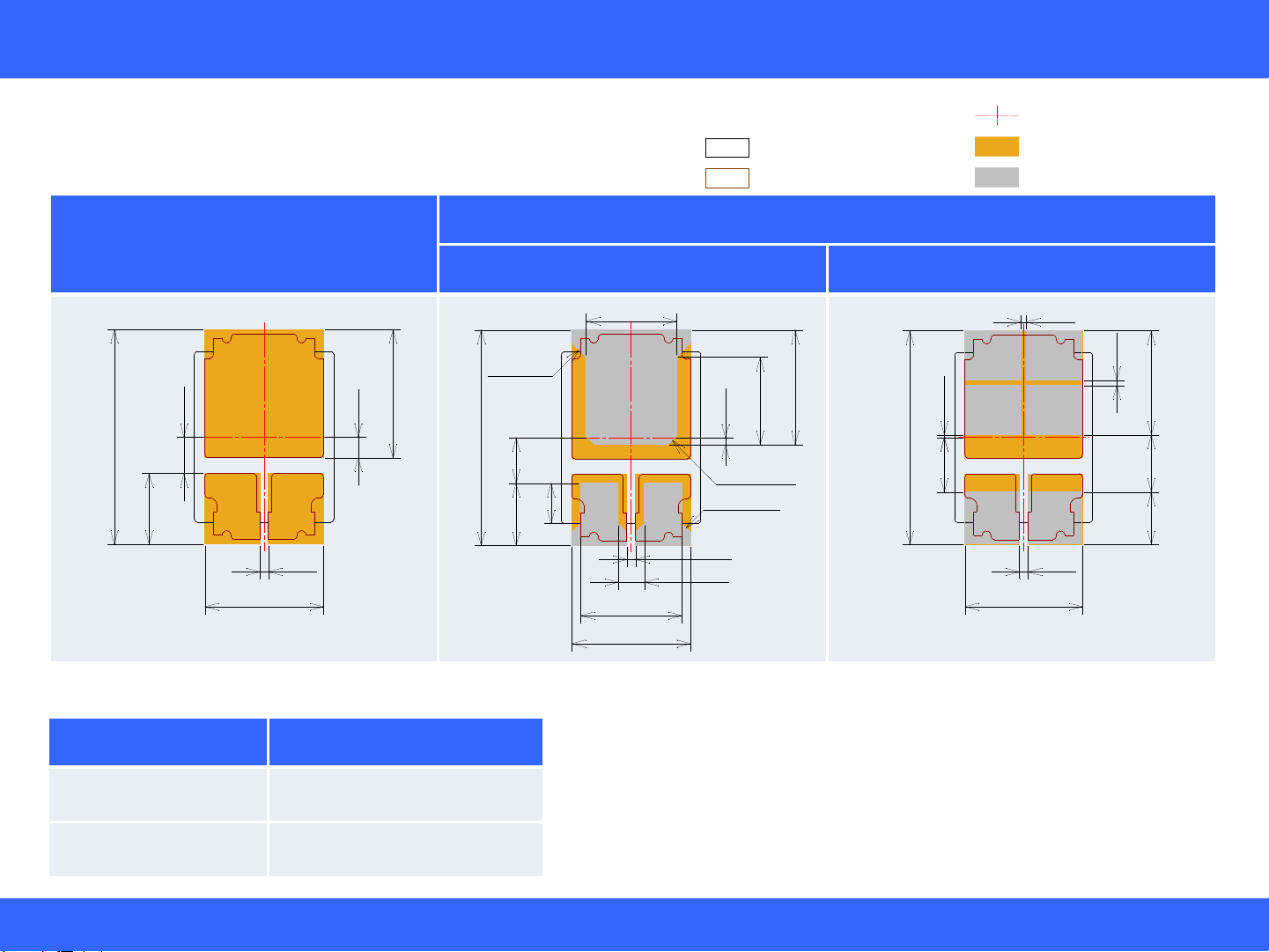
1. LED Outline Dimensions/Tape Dimensions
2. Handling Precautions
3. Design Recommendations for Optimal Amount of Solder
4. Precautions for Setting Up a Pick-and-Place Machine/Nozzle
5. Precautions When Reflow Soldering
Assembly Precautions
for the Nichia 193F Series LEDs

Light Emitting Diode
This document contains tentative information, Nichia may change the contents without notice.
2/14 SP-QR-C2-220184-1
Jun. 8, 2022
Assembly Precautions for the Nichia 193F Series LEDs
LED Embossed Carrier Tape
Weight: typ. 0.35g
(Unit: mm, Tolerance: ±0.1mm)
(単位 Unit: mm)
This product complies with RoHS Directive.
本製品はRoHS指令に適合しております。
(単位 Unit: mm, 公差 Tolerance: ±0.1)
No. STS-DA7-17892
Part No. NCSW193F
The dimension(s) in parentheses are for reference purposes.
括弧で囲まれた寸法は参考値です。
*
*
K A
保護素子
Protection Device
ダイヒートシンク
Die Heat Sink
A5.8
B6.8
0.9
1.4
2.2
5.7
7.1
0.9
Cathode Anode
ダイヒートシンク
Die Heat Sink
1.15±0.05
1.15±0.05
(2.65) 2.5
8
(1.95)
11.8
9.8
(9)
(7.2)
0.5
(2.8)
Cathode Mark
0.2 A
0.2 B
1.8 Max
0.5
0.9
1.27
項目 Item
パッケージ材質
Package Materials
内容 Description
黒色耐熱性ポリマー
Black Heat-resistant Polymer
電極材質
Electrodes Materials
ダイヒートシンク材質
Die Heat Sink
Materials
銅合金+金メッキ
Au-plated Copper Alloy
蛍光体板材質
Phosphor sheet
Materials
封止樹脂材質
Encapsulating Resin
Materials
シリコーン樹脂
Silicone Resin
銅合金+金メッキ
Au-plated Copper Alloy
蛍光体セラミックス
Phosphor Ceramics
質量
Weight 0.35g(TYP)
Dimensions do not include mold flash or metal burr.
バリは寸法に含まないものとします。
*
It may contain the products having the following ribbon shapes.
製品には以下のようなリボン形状が含まれます。
*
形状1
Shape1
形状2
Shape2
形状3
Shape3
カソードマーク
ダイヒートシンク
カソード
アノード
(単位 Unit: mm)
This product complies with RoHS Directive.
本製品はRoHS指令に適合しております。
(単位 Unit: mm, 公差 Tolerance: ±0.1)
No. STS-DA7-17892
Part No. NCSW193F
The dimension(s) in parentheses are for reference purposes.
括弧で囲まれた寸法は参考値です。
*
*
K A
保護素子
Protection Device
ダイヒートシンク
Die Heat Sink
A5.8
B6.8
0.9
1.4
2.2
5.7
7.1
0.9
Cathode Anode
ダイヒートシンク
Die Heat Sink
1.15±0.05
1.15±0.05
(2.65) 2.5
8
(1.95)
11.8
9.8
(9)
(7.2)
0.5
(2.8)
Cathode Mark
0.2 A
0.2 B
1.8 Max
0.5
0.9
1.27
項目 Item
パッケージ材質
Package Materials
内容 Description
黒色耐熱性ポリマー
Black Heat-resistant Polymer
電極材質
Electrodes Materials
ダイヒートシンク材質
Die Heat Sink
Materials
銅合金+金メッキ
Au-plated Copper Alloy
蛍光体板材質
Phosphor sheet
Materials
封止樹脂材質
Encapsulating Resin
Materials
シリコーン樹脂
Silicone Resin
銅合金+金メッキ
Au-plated Copper Alloy
蛍光体セラミックス
Phosphor Ceramics
質量
Weight 0.35g(TYP)
Dimensions do not include mold flash or metal burr.
バリは寸法に含まないものとします。
*
It may contain the products having the following ribbon shapes.
製品には以下のようなリボン形状が含まれます。
*
形状1
Shape1
形状2
Shape2
形状3
Shape3
1
2
Part No. Nxxx193x
No. STS-DA7-17893
(単位 Unit: mm)
テーピング部 Tape
トレーラ部/リーダ部 Trailer and Leader
* 数量は1リールにつき 1800個入りです。
Reel Size: 1800pcs
* 実装作業の中断などでエンボスキャリアテープをリールに巻き取る場合、
エンボスキャリアテープを強く(10N以上)締めないで下さい。
LEDがカバーテープに貼り付く可能性があります。
When the tape is rewound due to work interruptions,
no more than 10N should be applied to
the embossed carrier tape.
The LEDs may stick to the top cover tape.
* 実装作業の開始・中断・再開作業時などでリボンに過度な荷重を加えると、
リボンが変形し、不灯・不具合の原因になる可能性があります。
Ensure that when starting or suspending or resuming the
mounting work, excessive force is not applied to the ribbon.
Otherwise, it may cause damage to the ribbon, which cause
the LED to malfunction(e.g. the LED not to illuminate).
2±0.1 4±0.1
Φ1.5+0.1
1.75±0.1
11.5±0.1
12±0.1
-0
24+0.3
-0.1
トップカバーテープ
引き出し方向
Embossed Carrier Tape
エンボスキャリアテープ
Top Cover Tape
Feed
Direction
Trailer 160mm MIN(Empty Pockets)
リーダ部最小400mm
Leader without Top Cover Tape 400mm MIN
LED装着部
Loaded Pockets
引き出し部最小100mm(空部)
Leader with Top Cover Tape
100mm MIN(Empty Pocket)
トレーラ部最小160mm(空部)
リール部 Reel
Φ100±1
25.5±1
29.5±1
330±2
ラベル
Label
12.05±0.1
0.25±0.05
1.95±0.1
1±0.1
2±0.1
2±0.1
8.25±0.1
2±0.1
2±0.1
Φ2.05±0.05
(0.5 クロスバー凹部)
(0.5 Crossbar Recess)
(0.5 クロスバー凹部)
Feeding
Direction (Unit: mm)
1. LED Outline Dimensions/Tape Dimensions
Table 1. NCSW193F Product Specifications
Direction of the LED in the embossed carrier tape pocket: the
cathode faces the feeding direction of the tape as shown in the
figure above.
Cathode Anode
Die Heatsink
Cathode Mark
(0.5 Crossbar Recess)
1The centerline of the emitting area in the lateral direction is parallel to B; the
deviation in distance between the centerline and B is within ±0.1mm.
2The deviation of the centerline of the emitting area in the longitudinal
direction from the centerline of the die heatsink in the longitudinal direction is
within ±0.1mm.

Light Emitting Diode
This document contains tentative information, Nichia may change the contents without notice.
3/14 SP-QR-C2-220184-1
Jun. 8, 2022
Assembly Precautions for the Nichia 193F Series LEDs
LED Embossed Carrier Tape
Weight: typ. 0.36g
(Unit: mm, Tolerance: ±0.1mm)
(単位 Unit: mm)
This product complies with RoHS Directive.
本製品はRoHS指令に適合しております。
(単位 Unit: mm, 公差 Tolerance: ±0.1)
No. STS-DA7-17856A
Part No. NC2W193F
The dimension(s) in parentheses are for reference purposes.
括弧で囲まれた寸法は参考値です。
*
*
K A
保護素子
Protection Device
ダイヒートシンク
Die Heat Sink
A5.8
B6.8
0.9
1.4
2.2
5.7
7.1
0.9
Cathode Anode
ダイヒートシンク
Die Heat Sink
1.15±0.05
2.3±0.05
(2.2) 2.5
(3.2)
(2.4)
11.8
8
(7.2)
0.5
9.8
(9)
Cathode Mark
0.2 B 0.2 A
1.27
0.5
0.9
1.8 Max
項目 Item
パッケージ材質
Package Materials
内容 Description
黒色耐熱性ポリマー
Black Heat-resistant Polymer
電極材質
Electrodes Materials
ダイヒートシンク材質
Die Heat Sink
Materials
銅合金+金メッキ
Au-plated Copper Alloy
蛍光体板材質
Phosphor sheet
Materials
封止樹脂材質
Encapsulating Resin
Materials
シリコーン樹脂
Silicone Resin
銅合金+金メッキ
Au-plated Copper Alloy
蛍光体セラミックス
Phosphor Ceramics
質量
Weight 0.36g(TYP)
Dimensions do not include mold flash or metal burr.
バリは寸法に含まないものとします。
*
It may contain the products having the following ribbon shapes.
製品には以下のようなリボン形状が含まれます。
*
形状1
Shape1
形状2
Shape2
形状3
Shape3
カソードマーク
ダイヒートシンク
カソード
アノード
Part No. Nxxx193x
No. STS-DA7-17868A
(単位 Unit: mm)
テーピング部 Tape
トレーラ部/リーダ部 Trailer and Leader
* 数量は1リールにつき 1800個入りです。
Reel Size: 1800pcs
* 実装作業の中断などでエンボスキャリアテープをリールに巻き取る場合、
エンボスキャリアテープを強く(10N以上)締めないで下さい。
LEDがカバーテープに貼り付く可能性があります。
When the tape is rewound due to work interruptions,
no more than 10N should be applied to
the embossed carrier tape.
The LEDs may stick to the top cover tape.
* 実装作業の開始・中断・再開作業時などでリボンに過度な荷重を加えると、
リボンが変形し、不灯・不具合の原因になる可能性があります。
Ensure that when starting or suspending or resuming the
mounting work, excessive force is not applied to the ribbon.
Otherwise, it may cause damage to the ribbon, which cause
the LED to malfunction(e.g. the LED not to illuminate).
2±0.1 4±0.1
Φ1.5+0.1
1.75±0.1
11.5±0.1
12±0.1
-0
24+0.3
-0.1
トップカバーテープ
引き出し方向
Embossed Carrier Tape
エンボスキャリアテープ
Top Cover Tape
Feed
Direction
Trailer 160mm MIN(Empty Pockets)
リーダ部最小400mm
Leader without Top Cover Tape 400mm MIN
LED装着部
Loaded Pockets
引き出し部最小100mm(空部)
Leader with Top Cover Tape
100mm MIN(Empty Pocket)
トレーラ部最小160mm(空部)
リール部 Reel
Φ100±1
25.5±1
29.5±1
330±2
ラベル
Label
12.05±0.1
0.25±0.05
1.95±0.1
1±0.1
2±0.1
2±0.1
8.25±0.1
2±0.1
2±0.1
Φ2.05±0.05
(0.5 クロスバー凹部)
(0.5 Crossbar Recess)
(0.5 クロスバー凹部)
1
2
Feeding
Direction (Unit: mm)
1. LED Outline Dimensions/Tape Dimensions
Table 2. NC2W193F Product Specifications
Direction of the LED in the embossed carrier tape pocket: the
cathode faces the feeding direction of the tape as shown in the
figure above.
Cathode Anode
Die Heatsink
Cathode Mark
(0.5 Crossbar Recess)
1The centerline of the emitting area in the lateral direction is parallel to B; the
deviation in distance between the centerline and B is within ±0.1mm.
2The deviation of the centerline of the emitting area in the longitudinal
direction from the centerline of the die heatsink in the longitudinal direction is
within ±0.1mm.

Light Emitting Diode
This document contains tentative information, Nichia may change the contents without notice.
4/14 SP-QR-C2-220184-1
Jun. 8, 2022
Assembly Precautions for the Nichia 193F Series LEDs
LED Embossed Carrier Tape
Weight: typ. 0.37g
(Unit: mm, Tolerance: ±0.1mm)
(単位 Unit: mm)
This product complies with RoHS Directive.
本製品はRoHS指令に適合しております。
(単位 Unit: mm, 公差 Tolerance: ±0.1)
No. STS-DA7-17846A
Part No. NC3W193F
The dimension(s) in parentheses are for reference purposes.
括弧で囲まれた寸法は参考値です。
*
*
K A
保護素子
Protection Device
ダイヒートシンク
Die Heat Sink
A5.8
B6.8
0.9
1.4
2.2
5.7
7.1
0.9
Cathode Anode
ダイヒートシンク
Die Heat Sink
3.45±0.05
1.15±0.05
(2.2) 2.5
(2.4)
(4)
11.8
8
(7.2)
0.5
9.8
(9)
Cathode Mark
0.2 B 0.2 A
1.27
0.5
0.9
1.8 Max
項目 Item
パッケージ材質
Package Materials
内容 Description
黒色耐熱性ポリマー
Black Heat-resistant Polymer
電極材質
Electrodes Materials
ダイヒートシンク材質
Die Heat Sink
Materials
銅合金+金メッキ
Au-plated Copper Alloy
蛍光体板材質
Phosphor sheet
Materials
封止樹脂材質
Encapsulating Resin
Materials
シリコーン樹脂
Silicone Resin
銅合金+金メッキ
Au-plated Copper Alloy
蛍光体セラミックス
Phosphor Ceramics
質量
Weight 0.37g(TYP)
Dimensions do not include mold flash or metal burr.
バリは寸法に含まないものとします。
*
It may contain the products having the following ribbon shapes.
製品には以下のようなリボン形状が含まれます。
*
形状1
Shape1
形状2
Shape2
形状3
Shape3
カソードマーク
ダイヒートシンク
カソード
アノード
Part No. Nxxx193x
No. STS-DA7-17847A
(単位 Unit: mm)
テーピング部 Tape
トレーラ部/リーダ部 Trailer and Leader
* 数量は1リールにつき 1800個入りです。
Reel Size: 1800pcs
* 実装作業の中断などでエンボスキャリアテープをリールに巻き取る場合、
エンボスキャリアテープを強く(10N以上)締めないで下さい。
LEDがカバーテープに貼り付く可能性があります。
When the tape is rewound due to work interruptions,
no more than 10N should be applied to
the embossed carrier tape.
The LEDs may stick to the top cover tape.
* 実装作業の開始・中断・再開作業時などでリボンに過度な荷重を加えると、
リボンが変形し、不灯・不具合の原因になる可能性があります。
Ensure that when starting or suspending or resuming the
mounting work, excessive force is not applied to the ribbon.
Otherwise, it may cause damage to the ribbon, which cause
the LED to malfunction(e.g. the LED not to illuminate).
2±0.1 4±0.1
Φ1.5+0.1
1.75±0.1
11.5±0.1
12±0.1
-0
24+0.3
-0.1
トップカバーテープ
引き出し方向
Embossed Carrier Tape
エンボスキャリアテープ
Top Cover Tape
Feed
Direction
Trailer 160mm MIN(Empty Pockets)
リーダ部最小400mm
Leader without Top Cover Tape 400mm MIN
LED装着部
Loaded Pockets
引き出し部最小100mm(空部)
Leader with Top Cover Tape
100mm MIN(Empty Pocket)
トレーラ部最小160mm(空部)
リール部 Reel
Φ100±1
25.5±1
29.5±1
330±2
ラベル
Label
12.05±0.1
0.25±0.05
1.95±0.1
1±0.1
2±0.1
2±0.1
8.25±0.1
2±0.1
2±0.1
Φ2.05±0.05
(0.5 クロスバー凹部)
(0.5 Crossbar Recess)
(0.5 クロスバー凹部)
1
2
Feeding
Direction (Unit: mm)
1. LED Outline Dimensions/Tape Dimensions
Table 3. NC3W193F Product Specifications
Direction of the LED in the embossed carrier tape pocket: the
cathode faces the feeding direction of the tape as shown in the
figure above.
Cathode Anode
Die Heatsink
Cathode Mark
(0.5 Crossbar Recess)
1The centerline of the emitting area in the lateral direction is parallel to B; the
deviation in distance between the centerline and B is within ±0.1mm.
2The deviation of the centerline of the emitting area in the longitudinal
direction from the centerline of the die heatsink in the longitudinal direction is
within ±0.1mm.

Light Emitting Diode
This document contains tentative information, Nichia may change the contents without notice.
5/14 SP-QR-C2-220184-1
Jun. 8, 2022
Assembly Precautions for the Nichia 193F Series LEDs
LED Embossed Carrier Tape
Weight: typ. 0.38g
(Unit: mm, Tolerance: ±0.1mm)
(単位 Unit: mm)
This product complies with RoHS Directive.
本製品はRoHS指令に適合しております。
(単位 Unit: mm, 公差 Tolerance: ±0.1)
No. STS-DA7-17901
Part No. NC4W193F
The dimension(s) in parentheses are for reference purposes.
括弧で囲まれた寸法は参考値です。
*
*
K
保護素子
Protection Device
A
ダイヒートシンク
Die Heat Sink
A5.8
B6.8
0.9
1.4
2.2
5.7
7.1
0.9
Cathode Anode
ダイヒートシンク
Die Heat Sink
(9)
9.8
0.5
(7.2)
8
11.8
(2.4)
(5.1)
2.5
(2.2)
1.15±0.05
4.6±0.05
Cathode Mark
0.2 A
0.2 B
1.27
0.5
0.9
1.8 Max
項目 Item
パッケージ材質
Package Materials
内容 Description
黒色耐熱性ポリマー
Black Heat-resistant Polymer
電極材質
Electrodes Materials
ダイヒートシンク材質
Die Heat Sink
Materials
銅合金+金メッキ
Au-plated Copper Alloy
蛍光体板材質
Phosphor sheet
Materials
封止樹脂材質
Encapsulating Resin
Materials
シリコーン樹脂
Silicone Resin
銅合金+金メッキ
Au-plated Copper Alloy
蛍光体セラミックス
Phosphor Ceramics
質量
Weight 0.38g(TYP)
Dimensions do not include mold flash or metal burr.
バリは寸法に含まないものとします。
*
It may contain the products having the following ribbon shapes.
製品には以下のようなリボン形状が含まれます。
*
形状1
Shape1
形状2
Shape2
形状3
Shape3
カソードマーク
ダイヒートシンク
カソード
アノード
Part No. Nxxx193x
No. STS-DA7-17902
(単位 Unit: mm)
テーピング部 Tape
トレーラ部/リーダ部 Trailer and Leader
* 数量は1リールにつき 1800個入りです。
Reel Size: 1800pcs
* 実装作業の中断などでエンボスキャリアテープをリールに巻き取る場合、
エンボスキャリアテープを強く(10N以上)締めないで下さい。
LEDがカバーテープに貼り付く可能性があります。
When the tape is rewound due to work interruptions,
no more than 10N should be applied to
the embossed carrier tape.
The LEDs may stick to the top cover tape.
* 実装作業の開始・中断・再開作業時などでリボンに過度な荷重を加えると、
リボンが変形し、不灯・不具合の原因になる可能性があります。
Ensure that when starting or suspending or resuming the
mounting work, excessive force is not applied to the ribbon.
Otherwise, it may cause damage to the ribbon, which cause
the LED to malfunction(e.g. the LED not to illuminate).
2±0.1 4±0.1
Φ1.5+0.1
1.75±0.1
11.5±0.1
12±0.1
-0
トップカバーテープ
引き出し方向
Embossed Carrier Tape
エンボスキャリアテープ
Top Cover Tape
Feed
Direction
Trailer 160mm MIN(Empty Pockets)
リーダ部最小400mm
Leader without Top Cover Tape 400mm MIN
LED装着部
Loaded Pockets
引き出し部最小100mm(空部)
Leader with Top Cover Tape
100mm MIN(Empty Pocket)
トレーラ部最小160mm(空部)
リール部 Reel
Φ100±1
25.5±1
29.5±1
330±2
ラベル
Label
12.05±0.1
0.25±0.05
1.95±0.1
1±0.1
2±0.1
2±0.1
8.25±0.1
2±0.1
2±0.1
24+0.3
-0.1
Φ2.05±0.05
(0.5 クロスバー凹部)
(0.5 Crossbar Recess)
(0.5 クロスバー凹部)
1
2
Feeding
Direction (Unit: mm)
1. LED Outline Dimensions/Tape Dimensions
Table 4. NC4W193F Product Specifications
Direction of the LED in the embossed carrier tape pocket: the
cathode faces the feeding direction of the tape as shown in the
figure above.
Cathode Anode
Die Heatsink
Cathode Mark
(0.5 Crossbar Recess)
1The centerline of the emitting area in the lateral direction is parallel to B; the
deviation in distance between the centerline and B is within ±0.1mm.
2The deviation of the centerline of the emitting area in the longitudinal
direction from the centerline of the die heatsink in the longitudinal direction is
within ±0.1mm.

Light Emitting Diode
This document contains tentative information, Nichia may change the contents without notice.
6/14 SP-QR-C2-220184-1
Jun. 8, 2022
Assembly Precautions for the Nichia 193F Series LEDs
LED Embossed Carrier Tape
Weight: typ. 0.38g
(Unit: mm, Tolerance: ±0.1mm)
Part No. Nxxx193x
No. STS-DA7-17873
(単位 Unit: mm)
テーピング部 Tape
トレーラ部/リーダ部 Trailer and Leader
* 数量は1リールにつき 1800個入りです。
Reel Size: 1800pcs
* 実装作業の中断などでエンボスキャリアテープをリールに巻き取る場合、
エンボスキャリアテープを強く(10N以上)締めないで下さい。
LEDがカバーテープに貼り付く可能性があります。
When the tape is rewound due to work interruptions,
no more than 10N should be applied to
the embossed carrier tape.
The LEDs may stick to the top cover tape.
* 実装作業の開始・中断・再開作業時などでリボンに過度な荷重を加えると、
リボンが変形し、不灯・不具合の原因になる可能性があります。
Ensure that when starting or suspending or resuming the
mounting work, excessive force is not applied to the ribbon.
Otherwise, it may cause damage to the ribbon, which cause
the LED to malfunction(e.g. the LED not to illuminate).
2±0.1 4±0.1
Φ1.5+0.1
1.75±0.1
11.5±0.1
12±0.1
-0
24+0.3
-0.1
トップカバーテープ
引き出し方向
Embossed Carrier Tape
エンボスキャリアテープ
Top Cover Tape
Feed
Direction
Trailer 160mm MIN(Empty Pockets)
リーダ部最小400mm
Leader without Top Cover Tape 400mm MIN
LED装着部
Loaded Pockets
引き出し部最小100mm(空部)
Leader with Top Cover Tape
100mm MIN(Empty Pocket)
トレーラ部最小160mm(空部)
リール部 Reel
Φ100±1
25.5±1
29.5±1
330±2
ラベル
Label
12.05±0.1
0.25±0.05
1.95±0.1
1±0.1
2±0.1
2±0.1
8.25±0.1
2±0.1
2±0.1
Φ2.05±0.05
(0.5 クロスバー凹部)
(0.5 Crossbar Recess)
(0.5 クロスバー凹部)
(単位 Unit: mm)
This product complies with RoHS Directive.
本製品はRoHS指令に適合しております。
(単位 Unit: mm, 公差 Tolerance: ±0.1)
No. STS-DA7-17872
Part No. NC5W193F
The dimension(s) in parentheses are for reference purposes.
括弧で囲まれた寸法は参考値です。
*
*
K
保護素子
Protection Device
A
ダイヒートシンク
Die Heat Sink
A5.8
B6.8
0.9
1.4
2.2
5.7
7.1
0.9
Cathode Anode
ダイヒートシンク
Die Heat Sink
5.75±0.05
1.15±0.05
(2.2) 2.5
(6.1)
(2.4)
11.8
8
(7.2)
0.5
9.8
(9)
Cathode Mark
0.2 B0.2 A
1.27
0.5
0.9
1.8 Max
項目 Item
パッケージ材質
Package Materials
内容 Description
黒色耐熱性ポリマー
Black Heat-resistant Polymer
電極材質
Electrodes Materials
ダイヒートシンク材質
Die Heat Sink
Materials
銅合金+金メッキ
Au-plated Copper Alloy
蛍光体板材質
Phosphor sheet
Materials
封止樹脂材質
Encapsulating Resin
Materials
シリコーン樹脂
Silicone Resin
銅合金+金メッキ
Au-plated Copper Alloy
蛍光体セラミックス
Phosphor Ceramics
質量
Weight 0.38g(TYP)
Dimensions do not include mold flash or metal burr.
バリは寸法に含まないものとします。
*
It may contain the products having the following ribbon shapes.
製品には以下のようなリボン形状が含まれます。
*
形状1
Shape1
形状2
Shape2
形状3
Shape3
カソードマーク
ダイヒートシンク
カソード
アノード
1
2
Feeding
Direction (Unit: mm)
1. LED Outline Dimensions/Tape Dimensions
Table 5. NC5W193F Product Specifications
Direction of the LED in the embossed carrier tape pocket: the
cathode faces the feeding direction of the tape as shown in the
figure above.
Cathode Anode
Die Heatsink
Cathode Mark
(0.5 Crossbar Recess)
1The centerline of the emitting area in the lateral direction is parallel to B; the
deviation in distance between the centerline and B is within ±0.1mm.
2The deviation of the centerline of the emitting area in the longitudinal
direction from the centerline of the die heatsink in the longitudinal direction is
within ±0.1mm.

Light Emitting Diode
This document contains tentative information, Nichia may change the contents without notice.
7/14 SP-QR-C2-220184-1
Jun. 8, 2022
Assembly Precautions for the Nichia 193F Series LEDs
Caution: Do not touch the
prohibited area.
Suggestion: Grab/hold the LEDs with
tweezers by the package.
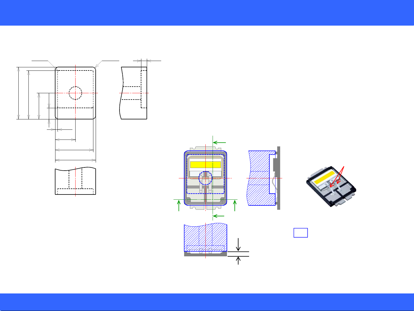
2.1 Prohibited area
Do not touch the prohibited area shown in Figure 1. This may cause the LED malfunction (e.g. the LED not to
illuminate).
2.2 Handling with bare hands
Do not handle the LEDs with bare hands:
- this may contaminate the LED surface and have an effect on the optical characteristics,
- this may cause the LED to deform or to be damaged causing a catastrophic failure (i.e. the LED not to
illuminate),
- the electrodes and/or the die heatsink may cause injuries when the LED is handled with bare hands.
2.3 Handling with tweezers
Ensure that when handling the LEDs with tweezers, grab/hold the LEDs by the package (i.e. the black part) and
ensure that excessive force is not applied to the LED. Otherwise, it may cause damage to the LED (e.g. cut,
scratch, chip, crack, etc.) and have an effect on the optical characteristics and/or the reliability. See Figure 2.
2.4 ESD Precautions
The LEDs are sensitive to transient excessive voltages (e.g. ESD, lightning surge). If this excessive voltage
occurs in the circuit, it may cause the LED to be damaged causing issues (e.g. the LED to become dimmer or
not to illuminate [i.e. catastrophic failure]). When handling the LEDs, ensure that necessary measures have
been taken to protect them from transient excess voltages.
2.5 Stacking assembled PCBs together
Do not stack assembled PCBs together. Otherwise, it may cause damage to the LED (e.g. cut, scratch, chip,
crack, etc.) and have an effect on the optical characteristics and/or the reliability.
2.6 Storage
The storage/packaging requirements for the Nichia 193F Series LEDs are comparable to JEDEC Moisture
Sensitivity Level (MSL) 2 or equivalent. Nichia used IPC/JEDEC STD-020 as a reference to rate the MSL of the
LEDs. Table 6 shows the required storage conditions for the LEDs.
Conditions Temperature Humidity Time
Storage
Before Opening Aluminum Bag ≤30℃≤90%RH Within 1 Year from Delivery Date
After Opening Aluminum Bag ≤30℃≤70%RH Within 1 Year Figure 2. Correct/Incorrect Examples
of Handling with Tweezers
Figure 1. Prohibited area
Prohibited
area
2. Handling Precautions
Table 6. Storage Conditions
Correct
Incorrect
Light Emitting Diode
This document contains tentative information, Nichia may change the contents without notice.
8/14 SP-QR-C2-220184-1
Jun. 8, 2022
Assembly Precautions for the Nichia 193F Series LEDs
Recommended Soldering Pad Pattern
Recommended Metal Solder Stencil Aperture
Pattern Recommended in the Specification Modified Pattern4
(Unit: mm) (Unit: mm) (Unit: mm)
Item Recommended Conditions
Metal Solder Stencil
(Thickness) 120μm
Solder Paste
(Composition) Sn-3.0Ag-0.5Cu
Center of the Soldering Pad
Pattern
Metal Solder Stencil Aperture
Soldering Pad Pattern
3. Design Recommendations for Optimal Amount of Solder
Soldering Pad Pattern/Metal Solder Stencil Aperture
Table 7. Recommended Soldering Pad Pattern/Metal Solder Stencil Aperture3
Table 8. Recommended Solder/Metal Solder Stencil Conditions3
6 .8
0 .5
2 .1
7 .35
1 .2
12 .3
4 .05
6 .8
0 .5
0 .3
0 .3
6
3 .3
3
3 .15 0 .15
12 .3
5 .2
2 .6
3 .55
12 .3
2 .3
5
6 .55
0 .5
1 .5
5 .8
6 .8
0 .4
2-C0 .8
4-C0 .5
2-C0 .5
Electrodes and Die Heatsink
Package Outline
3The recommended soldering pad pattern, metal solder stencil aperture, and thickness
of the metal solder stencil provided in Tables 7 and 8 have been determined under
Nichia’s conditions: ensure that there are no issues with the chosen assembly conditions
prior to use.
4If the aperture is large, the solder paste may not be applied evenly (i.e. thinner for the
middle area of the aperture) in the solder printing process causing the amount of the
solder paste applied to the soldering pad pattern to vary for each operation. This
modified pattern has four small apertures for the die heatsink instead of one large
aperture while the total area of the aperture is almost the same as that for the pattern
recommended in the specification.

Light Emitting Diode
This document contains tentative information, Nichia may change the contents without notice.
9/14 SP-QR-C2-220184-1
Jun. 8, 2022
Assembly Precautions for the Nichia 193F Series LEDs
Item Recommended Conditions/Specifications Cautions/Suggestions
Pick-and-place machine Modular mounter YS100 High-Speed General-Purpose Modular
(manufactured by Yamaha Motor Co., Ltd.)
Pick-and-place nozzle Nozzle specifically designed for the LEDs (see Figure 3) See “4.1 Pick-and-Place Nozzle” on Page 10 for details.
Tape-and-reel feeder Electrical (motorized) feeder Tape width: 24mm
Feeder pitch: 12mm
Top cover tape removal
position Immediately before pick-up See “4.2 Tape-and-Reel Feeder” on Page 11 for details.
Nozzle height for pick-up
operations
The contact surface of the nozzle head for pick
operations should be adjusted to 1.05mm below the
edge of the embossed carrier tape pocket.
See “4.3 Recommended Nozzle Height for Pick-up
Operations” on Page 11 for details.
Nozzle height for placement
operations (i.e. placement
depth)
0.2mm for the placement depth See “4.4 Recommended Nozzle Height for Placement
Operations (Placement Depth)” on Page 12 for details.
Imaging-based automatic
inspection
To locate the center of the LED, using the electrodes
and die heatsink as a reference is recommended.
See “4.5 Imaging-based Automatic Inspection" on Page
12 for details.
4. Precautions for Setting up a Pick-and-Place Machine/Nozzle
Table 9. Cautions/Suggestions for Setting up the Equipment
Light Emitting Diode
This document contains tentative information, Nichia may change the contents without notice.
10/14 SP-QR-C2-220184-1
Jun. 8, 2022
Assembly Precautions for the Nichia 193F Series LEDs
5 The height of the LED is the same for all the LEDs in
the 193F series.
1. Use a pick-and-place nozzle that does not come in contact with the bonding ribbons of
the LED. Figure 3 shows the recommended dimensions for the pick-and-place nozzle.
Ensure that the size and shape of the nozzle tip are appropriate for the LEDs. Otherwise,
this may damage the LED (i.e. scratch, chip, crack, deformation, etc.), affecting the optical
characteristics and/or the reliability, or causing the LED not to illuminate. This may also
lead to an incorrect pick up (i.e. the LED is picked up in a tilted position).
2. When setting the LED pick-up position, ensure that the center of the nozzle and the
center of the LED are aligned and that the nozzle is oriented correctly (see Figure 4).
If the nozzle does not pick up the LED at the center of the LED, and/or if the orientation
of the nozzle is incorrect, this may damage the LED (i.e. scratch, chip, crack, deformation,
etc.), affecting the optical characteristics and/or the reliability, or causing the LED not to
illuminate. This may also lead to an incorrect pick up (i.e. the LED is picked up in a tilted
position).
5 .1
9 .5
10 .2
7 .5
8
4
0 .5
2 .2
1 .1R0 .75
R0 .25
Figure 4. LED Pick-up Position (the NC5W193F LED is shown as an example.)
(Unit: mm)
Bonding Ribbons
A
A’
Pick-and-Place Nozzle
0.9mm 5
BB’
4.1 Pick-and-Place Nozzle
Figure 3. Recommended Nozzle Dimensions Cross-sectional
View along A-Aʼ
Cross-sectional View along B-Bʼ

Light Emitting Diode
This document contains tentative information, Nichia may change the contents without notice.
11/14 SP-QR-C2-220184-1
Jun. 8, 2022
Assembly Precautions for the Nichia 193F Series LEDs
1. For the tape-and-reel feeder, the tape width is set to
24mm and the feeder pitch is set to 12mm.
2. Use a tape-and-reel feeder that ensures it does not
create excessive vibrations causing assembly issues.
Example: Electric (motorized) feeder
3. It is recommended to remove the top cover tape at
the recommended position shown in Figure 5 (i.e.
immediately before LED pick-up).
4. When handling the reel of the LEDs, ensure that
excessive force is not applied to the bonding ribbons
of the LEDs. Otherwise, this may cause the ribbons to
deform causing the LED to be damaged or not to
illuminate.
Feeding Direction of the Embossed Carrier Tape
LED Pick up
position
Recommended
Top Cover Tape
Removal Position
Top Cover Tape
Feeder Cover
Pick-and-Place Nozzle
1.05mm below the edge
of the tape pocket (i.e.
Pick-up depth)
Pick-and-Place
Nozzle
Embossed Carrier Tape (Pocket)
LED
4.2 Tape-and-Reel Feeder
Figure 5. Recommended Top Cover Tape Removal Position
4.3 Recommended Nozzle Height for Pick-up Operations
Figure 6. Recommended Nozzle Height for Pick-up Operations
1. Ensure that the nozzle goes down onto the LED in the tape pocket until the tip
touches the package (i.e. the black part).
Pick-up depth: 1.05mm
Note: If the reference level for the nozzle setting is at the edge of the tape pocket.
2. The recommended nozzle height for pick-up operations has been determined by
Nichia under specific verification conditions (see Table 9) and may not function as
expected with some other pick-and-place machines. If the pick-up operations are
unstable even with using the recommended nozzle height, adjust the nozzle height
appropriately for the pick-and-place machine being used.
If the pick point of the nozzle is too high,
- it may cause insufficient suction power leading to picking errors (e.g. the
nozzle’s failure to pick/lift the LED into the air, incorrect picking causing the
LED to tilt when in the air).
If the pick point of the nozzle is too low,
- it may cause issues (e.g. causing the embossed carrier tape to shake, causing
the tape pocket to deform) leading to picking failure.

Light Emitting Diode
This document contains tentative information, Nichia may change the contents without notice.
12/14 SP-QR-C2-220184-1
Jun. 8, 2022
Assembly Precautions for the Nichia 193F Series LEDs
Figure 8. Example of Reference Point to Detect, Recognize, or Locate
the Electrodes/Die Heatsink
1. The nozzle should further press the LED 0.2mm onto the PCB from the
height where the LED first touches solder paste.
If the release point of the nozzle is too high,
- it may cause placement issues (e.g. the LED to stick to the nozzle
after placement, the LED to be mounted in an incorrect
place/rotated position, the LED to become soldered to the PCB in
a tilted position, etc.).
If the release point of the nozzle is too low,
- excessive forces may be applied to the LED during placement and
it may cause the LED to become damaged.
1. Nichia recommends using the electrodes and die heatsink as a reference
to locate the center of the LED.
2. If the imaging device has trouble detecting/recognizing the
electrodes/die heatsink, adjust the settings (i.e. the brightness of the
light, etc.) of the pick-and-place machine.
3. If an automatic polarity detector is used for the LEDs, set up the imaging
device to detect the empty space between the die heatsink and
electrodes (i.e. Polarity Detection/Recognition Point in Figure 8 to the
left). In the example in Figure 8, the equipment measures the brightness
of the empty space against the threshold to locate the electrodes
and/or determine the polarity.
Placement
Depth
0.2mm
Pick-and-Place Nozzle
PCB
LED
0.9mm
4.4 Recommended Nozzle Height for Placement Operations (Placement Depth)
Figure 7. Recommended Nozzle Height for Placement (Placement Depth)
4.5 Imaging-based Automatic Inspection
Electrode/Die Heatsink Location
Detection/Recognition Points
Polarity Detection/Recognition
Point
Light Emitting Diode
This document contains tentative information, Nichia may change the contents without notice.
13/14 SP-QR-C2-220184-1
Jun. 8, 2022
Assembly Precautions for the Nichia 193F Series LEDs
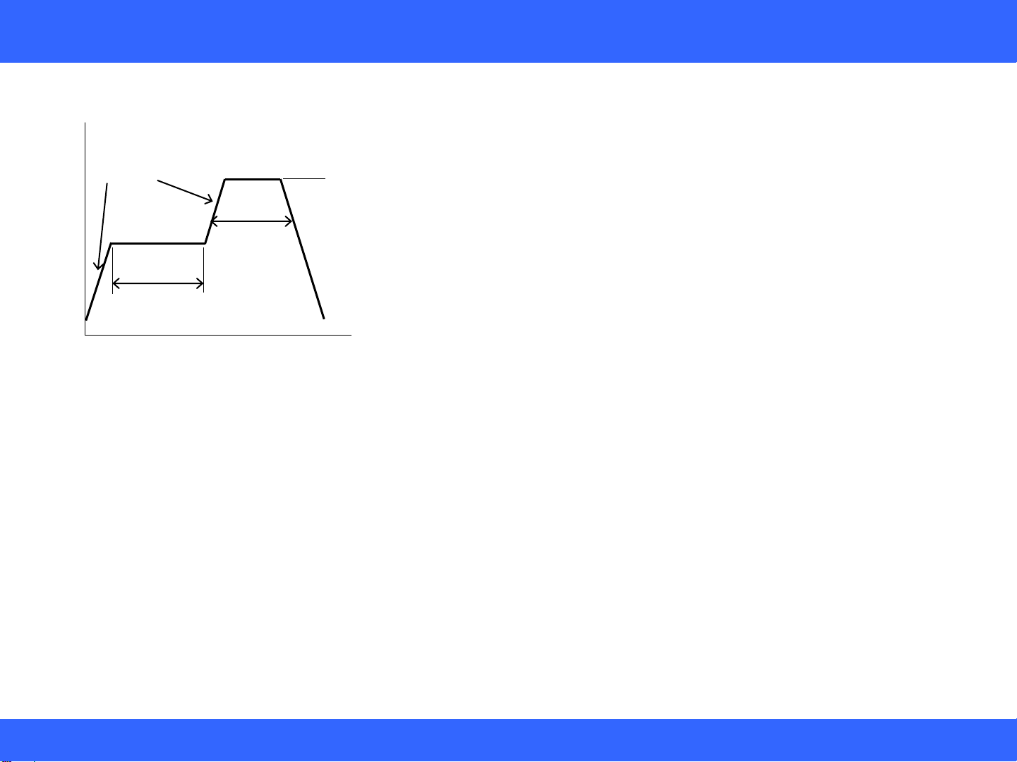
120sec Max
Pre-heat
180~200℃
260℃Max
10sec Max
220℃Max
60sec Max
1~5℃/sec
5. Precautions When Reflow Soldering
Figure 9. Recommended Reflow Soldering Condition
(Lead-free Solder)
1. Reflow soldering must not be performed more than twice.
2. Nichia recommends using the reflow soldering conditions detailed in Figure 9
to the left; use the recommended reflow conditions specified by the
manufacturer of the solder paste being used if it works better for the chosen
application.
Note: To ensure that these reflow conditions have no negative effect on the
LEDs, perform sufficient verification prior to use.
3. When cooling the LEDs from the peak temperature a gradual cooling slope is
recommended; do not cool the LEDs rapidly.
4. During reflow soldering, the heat and atmosphere in the reflow oven may cause
the optical characteristics to degrade. In particular, reflow soldering performed
with an air atmosphere may have a greater negative effect on the optical
characteristics than if a nitrogen atmosphere is used; Nichia recommends using
a nitrogen reflow atmosphere.

Light Emitting Diode
This document contains tentative information, Nichia may change the contents without notice.
14/14 SP-QR-C2-220184-1
Jun. 8, 2022
Disclaimer
Assembly Precautions for the Nichia 193F Series LEDs
This application note is a controlled document of Nichia Corporation (Nichia) published to provide technical information/data for
reference purposes only. By using this application note, the user agrees to the following:
•This application note has been prepared solely for reference on the subject matters incorporated within it and Nichia makes no
guarantee that customers will see the same results for their chosen application.
•The information/data contained herein are only typical examples of performances and/or applications for the product. Nichia
does not provide any guarantees or grant any license under or immunity from any intellectual property rights or other rights
held by Nichia or third parties.
•Nichia makes no representation or warranty, express or implied, as to the accuracy, completeness or usefulness of any
information contained herein. In addition, Nichia shall not be liable for any damages or losses arising out of exploiting, using,
or downloading or otherwise this document, or any other acts associated with this document.
•The content of this application note may be changed without any prior or subsequent notice.
•Copyrights and all other rights regarding the content of this document are reserved by Nichia or the right holders who have
permitted Nichia to use the content. Without prior written consent of Nichia, republication, reproduction, and/or redistribution
of the content of this document in any form or by any means, whether in whole or in part, including modifications or derivative
works hereof, is strictly prohibited.
NICHIA CORPORATION
491 Oka, Kaminaka-Cho, Anan-Shi,
TOKUSHIMA 774-8601, JAPAN
Phone: +81-884-22-2311 Fax: +81-884-21-0148
http://www.nichia.co.jp
This manual suits for next models
5
Table of contents
Popular Lighting Equipment manuals by other brands

Robert Juliat
Robert Juliat ZEP 360 manual

Ibiza
Ibiza HYPNO40-LED user manual

Lutron Electronics
Lutron Electronics EcoSystem 5-Series installation guide

GTD
GTD GTD-L1516P user manual

Home Accents Holiday
Home Accents Holiday TY315-1314 Use and care guide

Starling Technologies
Starling Technologies Pocket Spin Drift instruction manual


Welch Allyn
Welch Allyn GS 600 quick start guide

Piaa
Piaa 2000 Back-Up installation instructions

Larson Electronics
Larson Electronics GL-29000GB instruction manual

Poltronova
Poltronova Gherpe instructions

WDT
WDT Tele Indication Touch-V1 Operating and installation instructions

SUNSET
SUNSET F9806-30-3K Installation instructions manual