NXP Semiconductors AN5025 Installation and operating instructions

1 Introduction
This application note describes the usage of the DC-DC Switching Mode
Power Supply (SMPS) converter for the MKW4xZ/3xZ/3xA/2xZ families. This
document covers operating voltages, types of circuit operation, hardware
design guidelines, software configuration, and power capabilities.
2 MKW DC-DC converter
This application note is based on the MKW41Z technical data. For other part numbers, see the part-specific documentation as
operating conditions, features, specifications, and requirements may vary. For example, some parts do not support boost mode
(MKW36, MKW35, MKW37, MKW38).
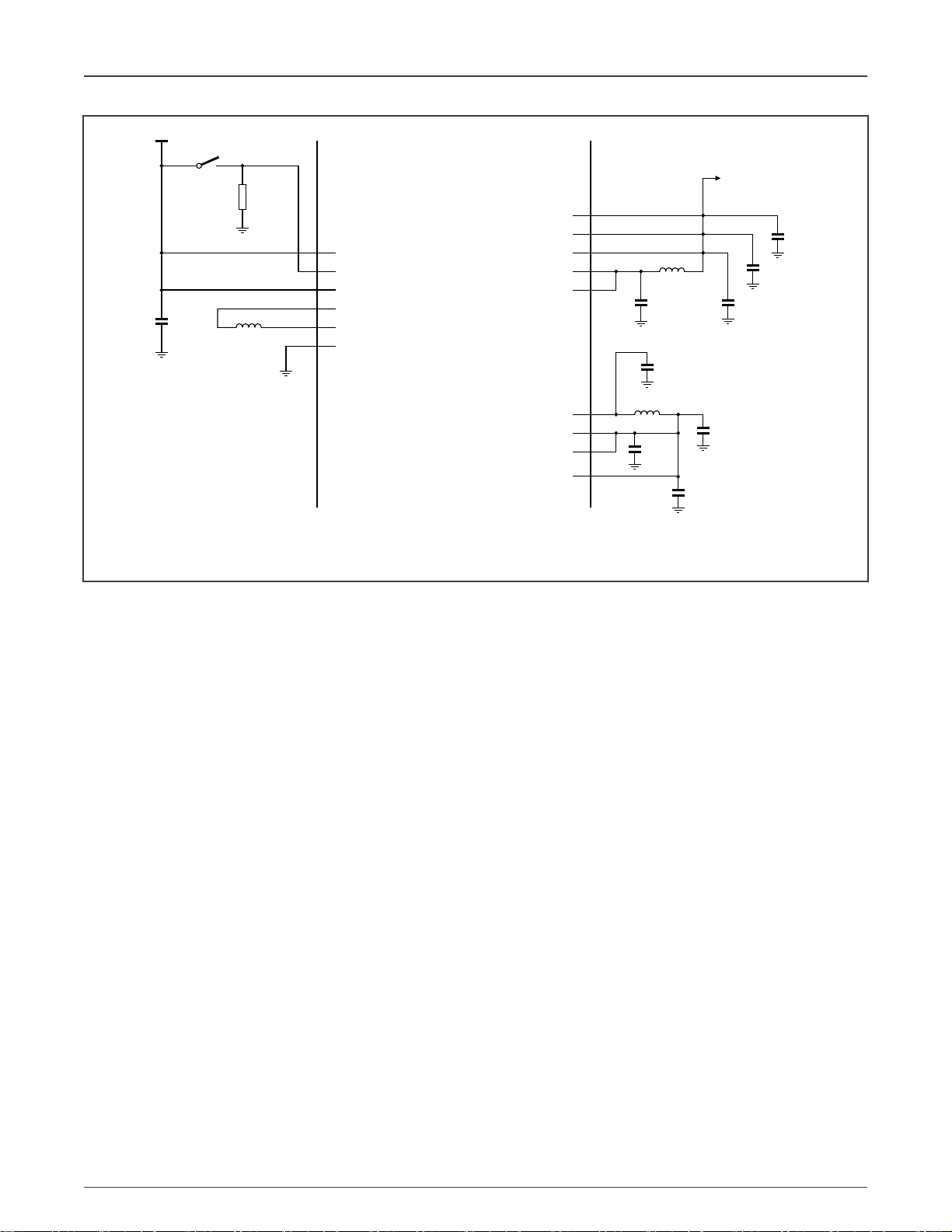
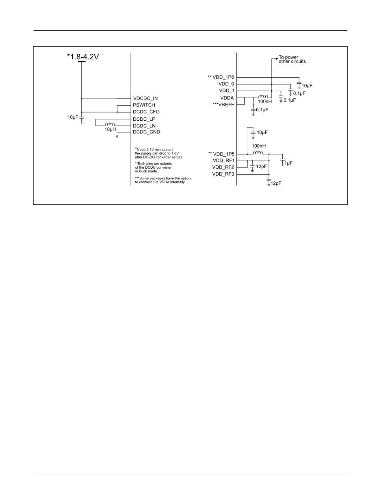
The DC-DC converter for MKW41Z is a dual output converter that supports three operating modes; Bypass, Buck, and Boost. In
Bypass mode, the DC-DC converter is disabled and the supply pins of the microcontroller must be supplied externally. In Buck
mode, the DC-DC converter is enabled and requires a DC supply in the range of 1.8 V to 4.2 V (during startup, the minimum supply
required is 2.1 V). In Boost mode, the DC-DC converter requires a DC supply in the range of 0.9 V to 1.795 V (during startup, the
minimum supply required is 1.1 V).
Startup and operating modes are configured with hardware selection through the DCDC_CFG and PSWITCH pins.
When the DC-DC converter is powered on, two outputs assume default voltage settings. By software, it is possible to change the
output voltages within the ranges shown in the table below, provided that, in Buck mode, for all input ranges the outputs are lower
than input voltage by 50 mV, or higher than input voltage by 50 mV when operating in Boost mode.
WARNING
VDD_1P8 must always be greater or equal to VDD_1P5. Otherwise, the internal protection diodes are forward biased, and may
cause electrical overstress, damaging the part.
Mode VDD1P8 VDD1P5
Default
Value
Range Default Value Range
Buck 1.8 V 1.71 V ≤ VDD_1P8 ≤ 3.50 V 1.5 V 1.425 V ≤ VDD_1P5 ≤ 1.65 V
Boost 1.8 V 1.71 V ≤ VDD_1P8 ≤ 3.50 V 1.8 V 1.425 V ≤ VDD_1P5 ≤ 2.0 V
The DC-DC operates in two different modes; Continuous and Pulsed mode. When operating in continuous mode, the internal
digital controls are constantly on and the operating frequency is 1/16th of the DC-DC reference frequency. In most applications,
the RF oscillator (or main oscillator) is used as the DC-DC reference frequency and this is a 32 MHz clock. This results in a 2 MHz
operating frequency. Some applications may use a 26 MHz crystal. This would result in a 1.625 MHz operating frequency. The
DC-DC also has an internal RC oscillator that can be used as a reference when the RF oscillator is not being used. The frequency
of this oscillator is 26 MHz.
Contents
1 Introduction......................................1
2 MKW DC-DC converter...................1
3 DC-DC Power modes......................2
4 DC-DC converter software setup.... 6
5 Hardware design Guidelines......... 16
6 Current estimation and efficiency
report.............................................21
7 Revision history.............................27
AN5025
MKW4xZ/3xZ/3xA/2xZ DC-DC Power Management
Rev. 3 — 04 June 2021 Application Note

In Pulsed mode, the DC-DC PWM is turned on until the output capacitor is charged to the configured high trigger limit. Then the
DC-DC PWM is temporarily turned off until the output voltage drops to the lower trigger limit, whereby a PWM burst then charges
the output capacitor again. In general, pulsed mode is entered when the SoC enters a low-power mode, and is in continuous mode
when the SoC is in a RUN mode. Software can configure which DC-DC mode (Continuous or Pulsed) is selected when entering
some low-power modes. Pulsed mode improves energy efficiency in low-power modes where the current does not exceed 0.5 mA.
VDD_1P8 should supply VDD1, VDD2, and VDDA through external PCB traces and, within the current capability, may also power
other circuits of the system. The VDD_1P5 is designed to supply just the Radio Frequency circuit. This power supply should be
externally connected to only the VDD_RF pins.
The DC-DC SMPS uses the voltage VDD_0/1 as feedback for the loop control of the VDD_1P8 output, so application hardware
designer must ensure the correct return signal without series resistance from VDD_1P8 to VDD_0/1.
It is not possible to configure the DC-DC for buck or boost modes while sourcing VDD_0/1 from an external source.
3 DC-DC Power modes
3.1 Bypass mode
In Bypass mode, the DC-DC converter is disabled. Both the VDD_1P8 and VDD_1P5 are inputs. MKW devices require individual
DC supply for the VDDx, VDDA, VDD_1P8, VDD_1P5, and VDD_RFx domains to be functional.
Below is the minimum recommended circuit configurations for DC-DC converter in Bypass mode.
VDCDC_IN
VDD_1P8
VDD_0
VDD_1
VDDA
VDD_1P5
VDD_RF1
VDD_RF2
VDD_RF3
* VREFH
DCDC_CFG
DCDC_LP
* Some packages have the
option to connect it to VDDA
internally
DCDC_LN
DCDC_GND
10 µF
PSWITCH
10
9
11
12
13
8
0.1 µF
1.71 - 3.6 V
1.45 - 3.6 V
1.71 - 3.6 V
0.1 µF
12 pF
0.1 µF
0.1 µF
0.1 µF
12 pF
10 µF
10 µF
Figure 1. MKW DC-DC in Bypass Mode
3.2 Buck mode
In Buck mode, the input voltage VDCDC_IN is converted to a lower voltage which is output to the VDD_1P8 and VDD_1P5 pins.
These pins are initialized to the below default startup values (after POR resets only), and then by software, those values may
be changed:
VDD_1P8 = 1.8 V and VDD_1P5 = 1.5 V
NXP Semiconductors
DC-DC Power modes
MKW4xZ/3xZ/3xA/2xZ DC-DC Power Management, Rev. 3, 04 June 2021
Application Note 2 / 28

In Buck mode, at steady state, the DC-DC converter accepts input voltages ranging from 1.8 V to 3.6 V (4.2 V for certain use cases
on KWx1Z; refer to the device-specific data sheet for conditions and limits). To guarantee the startup, it is necessary to have a
minimum input voltage of 2.1 V. The typical conversion efficiency is 90%.
There are two ways to start the DC-DC in Buck mode: Manual and Auto-Startup. The main difference is that on Auto-Startup,
when the VDCDC_IN voltage is applied, the DC-DC immediately starts the PWM, generating voltages on VDD_1P8 and VDD_1P5
outputs. In manual mode, the DC-DC is triggered to start after a pulse/level high on the PSWITCH.
It is possible to shut down the DC-DC after it has started, only in Buck Manual mode. The application must ensure that the
PSWITCH is not at a logic high level when the DC-DC is shut down. Otherwise, the DC-DC enters an abnormal state.
The tank capacitors connected to VDD_1P8 and VDD_1P5 must be in the range of 10 µF to 30 µF. Capacitor values outside this
range can have negative effects on the control loop response of the DC-DC converter. Larger capacitor value can save power
consumption in low-power mode due to a longer interval between refresh. However, if the capacitance is too great (greater than
30 uF) the DC-DC converter may not regulate properly. The lower ESR (Equivalent Series Resistance), the better for efficiency.
3.2.1 Buck Mode – Manual Startup
In this mode, the DC-DC is not automatically started upon the presence of voltage on VDCDC_IN. Instead, the DC-DC is started
after a pulse or level high on the PSWITCH pin; This pulse may come from a push button, switch, or externally generated by
another device. In either case, PSWITCH must be above the required startup level for longer than the DC-DC turn on time for the
DC-DC to start up correctly (refer to the device-specific data sheet for the PSWITCH VIH level and DC-DC turn on time). If an
external device is used, the application must guarantee the correct power-up sequence and voltage levels. This means:
• PSWITCH cannot be at a higher voltage than VDCDC_IN. Otherwise, the internal protection diode is forward biased,
damaging the device.
• The controlling circuit must keep PSWITCH at VIH voltage level with respect to VDCDC_IN. VIH voltage is defined in this
case as 0.7 x VDCDC_IN for 2.7 V <= VDCDC_IN or 0.75 x VDCDC_IN for 1.7 V <= VDD <= 2.7 V, unless otherwise
specified by the Voltage and current operating requirements table of the device-specific data sheet.
To shut down the DC-DC in this mode, the PSWITCH pin must be at a low logic level, and it is necessary to set the
DCDC_SW_SHUTDOWN bit at the same time as writing the unlock key 0x3E77 to the Unlock bits on register DCDC_REG4.
Below are the recommended hardware configurations for DC-DC converter in Buck Manual Start mode.
NXP Semiconductors
DC-DC Power modes
MKW4xZ/3xZ/3xA/2xZ DC-DC Power Management, Rev. 3, 04 June 2021
Application Note 3 / 28

VDCDC_IN
** VDD_1P8
To power
other circuits
VDD_0
VDD_1
VDDA
** VDD_1P5
VDD_RF1
VDD_RF2
VDD_RF3
** VREFH
DCDC_CFG
DCDC_LP
* Need 2.1 V min to start,
the supply can drop to 1.8 V
after DC-DC converter settles
** Both pins are outputs
of the DCDC converter
in Buck mode
*** Some packages have the
option to connect it to VDDA
internally
DCDC_LN
DCDC_GND
10 µH
10 µF
100 kΩ
SW1
*1.8 - 4.2 V
PSWITCH
0.1 µF
100 nH
0.1 µF
0.1 µF
10 µF
12 pF
1 µF
100 nH
12 pF
10 µF
*
Figure 2. MKW DC-DC in Buck mode (manual start)
3.2.2 Buck Mode – Auto start
This mode allows the DC-DC to automatically turn on immediately after power is applied to the device. Typical startup time is 2.3
ms and varies with the loading of the converter.
As the PSWITCH is always tied to VDCDC_IN, there is no possibility to turn off the DC-DC SMPS after it starts. If software attempts
to shut down the module, the device enters in an abnormal state, requiring a power cycle to recover the unit.
Below is the recommended circuit for DC-DC converter in Buck Auto Start mode:
NXP Semiconductors
DC-DC Power modes
MKW4xZ/3xZ/3xA/2xZ DC-DC Power Management, Rev. 3, 04 June 2021
Application Note 4 / 28

Figure 3. MKW DC-DC in Buck mode (auto start)
WARNING
This configuration is not recommended for Lithium-ion battery designs as over-discharging this type of battery may lead to
permanent damage, reducing its lifetime or causing degradation effects on performance.
3.3 Boost Mode
In Boost mode, the DC-DC converter accepts input voltage in the range of 0.9 V to 1.795 V. To guarantee startup, the DC-DC
requires a minimum of 1.1 V. The typical conversion efficiency is 90%.
In this mode, the DC-DC converter increases the input voltage, VDCDC_IN, to the below default startup values, and then by
software, those values may be changed:
VDD_1P8 = 1.8 V and VDD_1P5 = 1.8 V
Below is the recommended circuit for the DC-DC converter in Boost mode.
NXP Semiconductors
DC-DC Power modes
MKW4xZ/3xZ/3xA/2xZ DC-DC Power Management, Rev. 3, 04 June 2021
Application Note 5 / 28

VDCDC_IN
** VDD_1P8
To power
other circuits
VDD_0
VDD_1
VDDA
** VDD_1P5
VDD_RF1
VDD_RF2
VDD_RF3
** VREFH
DCDC_CFG
DCDC_LP
* Need 1.1 V min to start,
the supply can drop to 0.9 V
after DC-DC converter settles
** Both pins are outputs
of the DCDC converter
in Buck mode
*** Some packages have the
option to connect it to VDDA
internally
DCDC_LN
DCDC_GND
10 µH
10 µF
PSWITCH
0.1 µF
100 nH
0.1 µF
0.1 µF
10 µF
12 pF
1 µF
100 nH
12 pF
10 µF
*0.9 - 1.795 V
*
Figure 4. MKW DC-DC in Boost mode
3.4 Buck-Boost mode
The MKW DC-DC converter does not support Buck-Boost switching. Based on the battery voltage range for the system, the
application should be designed for either Buck or Boost configuration. It is not possible to switch modes on the fly. For example,
a hypothetical configuration circuit switching from buck to boost mode is not allowed. The DC-DC mode must change after the
power is turned off and the pin configuration correctly set.
4 DC-DC converter software setup
The DC-DC operates in two different modes; Continuous Mode and Pulsed Mode. In Continuous Mode, the control loop keeps
the PWM ON, constantly adjusting the pulse width to maintain the two output voltages.
The Pulsed Mode option periodically generates a PWM burst, recharging the bulk capacitors. When the voltage falls below the
configured threshold, the DC-DC module starts the PWM, and after voltage reaches the maximum threshold value, it turns off,
starting a new cycle. Pulsed mode is automatically entered whenever the MCU enters VLPR, VLPW, VLPS, LLS, or VLLSx modes.
Note that it is possible to, by software, select either Continuous or Pulsed Mode when entering VLPR, VLPW, or VLPS modes.
Below oscilloscope plots show the difference between Continuous and Pulsed modes.
NXP Semiconductors
DC-DC converter software setup
MKW4xZ/3xZ/3xA/2xZ DC-DC Power Management, Rev. 3, 04 June 2021
Application Note 6 / 28

Figure 5. Continuous Mode and Pulsed Modes
The two images on the left side show the continuous mode, the bottom images are the zoom of the upper ones. The images on
the right are screen captures of pulsed mode. Note that the VDD_1P8 presents a higher ripple due to DC-DC being turned off for
some time until minimum voltage threshold is reached. The ripple can be configured from -75 mV to +75 mV (in 25 mV increments)
via register bit fields DCDC_LP_STATE_HYS_L and DCDC_LP_STATE_HYS_H.
Note that these register bits should not be set to 0 mV offset at the same time as this will create a situation where the DC-DC
controller is active more than necessary and consumes more current than desired.
4.1 Application Initialization Requirements
To ensure optimum DC-DC operation, it is highly recommended to configure the Loop Control bits as below during the DC-DC
startup routine. These bits properly configure the internal hardware hysteresis parameters and improve transient supply ripple
and efficiency.
DCDC_REG1[DCDC_LOOPCTRL_DF_HST_THRESH] = 0 (This is already the reset value)
DCDC_REG1[DCDC_LOOPCTRL_CM_HST_THRESH] = 0 (This is already the reset value)
DCDC_REG1[DCDC_LOOPCTRL_EN_DF_HYST] = 1
DCDC_REG1[DCDC_LOOPCTRL_EN_CM_HYST] = 1
DCDC_REG2[DCDC_LOOPCTRL_HYST_SIGN] = 1
If Pulsed mode is used, the below bit must also be configured as follows:
NXP Semiconductors
DC-DC converter software setup
MKW4xZ/3xZ/3xA/2xZ DC-DC Power Management, Rev. 3, 04 June 2021
Application Note 7 / 28

DCDC_REG0[DCDC_LP_DF_CMP_ENABLE] = 1
If the DC-DC mode is Boost mode, it is necessary to set POSLIMIT_BOOST_IN to 0x12 after startup. During startup, this register
is set to a small value to limit voltage spikes and the software application must configure this bit field to the recommended value
to allow higher currents, especially when battery voltage is low.
DCDC_REG1[POSLIMIT_BOOST_IN] = 0x12
The DC-DC recommended software initialization and periodically voltage monitoring flowchart is given below:
Enable DCDC
Module Clock Gating
Set
POSLIMIT_BOOST_IN
to 0x12
Configure DCDC
LoopControl Registers and
DCDC_LP_DF_CMP ENABLE
Configure VDD_1P8
and VDD_1P5 output
targets
Is Boost mode
?
Enable Bandgap 1V
buffer
Measure the
VDCDC_IN with ADC
Measure the 1 V
reference bandgap
with ADC
Calculate VDCDC_IN
using bandgap
reference with 8 mV
LSB resolution
Disable
BATTMONITOR_EN_BATADJ
Update
DCDC_BATTMONITOR_BAT
T_VAL
Enable
BATTMONITOR_EN_BATADJ
Initialize ADC
Initialize Timer
Need to adjust
VBATT_DIV
?
no no
yes
Adjust
VBATT_DIV_CTRL
yes
Timer periodically runs this portion
Figure 6. Flowchart of DC-DC initialization
The period for the Timer to trigger the measurement of the VDCDC_IN is user controlled and depends on the applications
VDCDC_IN voltage dynamics. Every time the application expects a voltage change, it is recommended to execute the
DCDC_BATTMONITOR_BATT_VAL calibration routine.
It is expected that software monitors the VDCDC_IN periodically, using the SAR ADC, and adjust the DC-DC settings as required
to optimize the performance. Not adjusting the DCDC_BATTMONITOR_BATT_VAL when the VDCDC_IN voltage level has
changed could lead to erratic behavior. The DC-DC does not have a bypass circuit. So when configured for buck or boost, the
controller attempts to regulate the voltage no matter what the level of VDCDC_IN.
There are multiple ways to initialize the DC-DC: the DC-DC SDK (Software Development Kit) drivers (fsl_dcdc.c
and fsl_dcdc.h), direct register accesses, or the connectivity framework drivers. The DC-DC connectivity framework is
contained within the DCDC.c and DCDC.h files. Consider the below code segment from the MCUXpresso DC-DC
connectivity Framework as an example to initialize the DC-DC, Timer, and the ADC to set VDD1P8 to 1.8 V and
NXP Semiconductors
DC-DC converter software setup
MKW4xZ/3xZ/3xA/2xZ DC-DC Power Management, Rev. 3, 04 June 2021
Application Note 8 / 28

VDD1P5 to 1.5 V in Buck mode. This connectivity framework code can be found on the KW41 SDK examples
folder (SDK_2.2_MKW41Z512xxx4\boards\frdmkw41z\wireless_examples\smac\connectivity_test\bm\iar).
/* Default DCDC Mode used by the application */
#define APP_DCDC_MODE gDCDC_Mode_Buck_c
#define APP_DCDC_VBAT_MONITOR_INTERVAL (50000)
/**Configure the DCDC parameters though this const variable**/
const dcdcConfig_t mDCDCBuckDefaultConfig =
{
.vbatMin = 1800,
.vbatMax = 4200,
.dcdcMode = APP_DCDC_MODE,
.vBatMonitorIntervalMs = APP_DCDC_VBAT_MONITOR_INTERVAL,
.pfDCDCAppCallback = NULL, /* .pfDCDCAppCallback = DCDCCallback, */
.dcdcMcuVOutputTargetVal = gDCDC_McuV_OutputTargetVal_1_500_c,
.dcdc1P8OutputTargetVal = gDCDC_1P8OutputTargetVal_1_800_c
};
At the hardware initialization, call DCDC_Init function from the DCDC.c connectivity framework and the initialization, including the
ADC and timer setup, is executed.
//Init DCDC with VDD1P8 @ 1.8V
DCDC_Init(&mDCDCBuckDefaultConfig); // call to DCDC SDK Framework
4.2 Configuring Continuous mode
The DC-DC converter operates only in Continuous Mode when the MCU is in RUN, WAIT, and STOP modes. The DC-DC
converter may operate in Continuous mode or Pulsed mode through register selection when MCU is in VLPR, VLPW, and VLPS
modes. Continuous mode is not available for LLSx and VLLSx modes.
Depending on the use case and the low-power mode usage, it may be more efficient to select continuous mode rather than pulsed
mode. For current up to 0.5 mA, the recommendation is to measure the loading dynamics of the application to verify which mode
has better performance. Above 0.5 mA, the DC-DC must be configured for Continuous mode.
4.2.1 Target voltage adjustment
In Buck and Boost modes, the DC-DC converter output voltages are programmable. To adjust the target voltages of VDD_1P8
and VDD_1P5 in Continuous Mode, follow the below steps:
NXP Semiconductors
DC-DC converter software setup
MKW4xZ/3xZ/3xA/2xZ DC-DC Power Management, Rev. 3, 04 June 2021
Application Note 9 / 28

Below conditions must be met before starting output voltages adjustment:
bits
*Clear
and
Change target register bits
bit must be in set state (DCDC stable)
Read
Voltage adjustment complete
1 (DCDC stable)
0 (DCDC unstable)
and
and
1 - DCDC must be in Continuous Mode Operation
2 -
3 - Stepping control must be enabled*
Figure 7. Flowchart of target output voltage adjustment
*When the step bits are cleared, stepping control is enabled. It is mandatory to be in this state before adjusting the target output
voltage to avoid overshoot/undershoot, as this mode forces the DC-DC control loop to increase or decrease the voltage in steps
of 25mV until it reaches the target voltage.
4.3 Pulsed mode
The DC-DC converter can also operate in Pulsed mode when MCU is in VLPR, VLPW, and VLPS, which is software selectable.
The total current loading from VDD_1P8 must be less than 0.5 mA to select this mode.
Pulsed mode has better efficiency when loading is less than 0.5 mA. As mentioned before, larger tank capacitors on VDD_1P8
and VDD_1P5 lead to better efficiency in pulsed mode as the refresh time increases.
Pulsed mode is automatically set for the low-power modes; LLS3, LLS2, VLLS3, VLLS2, and VLLS1. The DC-DC converter is not
operational in VLLS0. Only Bypass mode is supported in VLLS0.
To ensure optimum DC-DC operation, it is mandatory to enable the low-power differential comparators, instead of common mode
sense. It reduces the ripple in pulsed mode, which means below bit must be set before entering in pulsed mode.
DCDC_REG0[DCDC_LP_DF_CMP_ENABLE] = 1
To guarantee correct regulation, before entering the Pulsed Mode, stepping must be disabled. It means that the below bits must
also be set:
DCDC_REG3 [DCDC_VDD1P8CTRL_DISABLE_STEP] = 1
DCDC_REG3 [DCDC_VDD1P5CTRL_DISABLE_STEP] = 1
4.3.1 Procedure to enter Pulsed mode
To enter Pulsed mode, follow the below steps:
• Perform these configurations during startup:
NXP Semiconductors
DC-DC converter software setup
MKW4xZ/3xZ/3xA/2xZ DC-DC Power Management, Rev. 3, 04 June 2021
Application Note 10 / 28

DCDC_REG0[VLPR_VLPW_CONFIG_DCDC_HP] = 0 (To enable pulsed mode on VLPR and VLPW)
DCDC_REG0[VLPS_CONFIG_DCDC_HP] = 0 (To enable pulsed mode on VLPS)
DCDC_REG0[DCDC_LP_DF_CMP_ENABLE] = 1 (Needed configuration to reduce ripple and to avoid voltage falling below
minimum limit)
Application software:
• Stepping must be disabled before entering Pulsed Mode:
DCDC_REG3[DCDC_VDD1P8CTRL_DISABLE_STEP] = 1 and DCDC_REG3[DCDC_VDD1P5CTRL_DISABLE_STEP] = 1
• Call user application low-power mode routine
There is no need to re-enable stepping after leaving Pulsed Mode. If there is a need to change the output voltages; VDD_1P8 and
VDD_1P5, the stepping must be re-enabled.
Consider the below code segment using SDK 2.x, instead of the Connectivity Framework, as an example to set Pulsed Mode when
entering low-power mode.
/** DCDC Low power configuration structure **/
dcdc_low_power_config_t dcdc_Low_Power_Config =
{
.workModeInVLPRW = kDCDC_WorkInPulsedMode,
.workModeInVLPS = kDCDC_WorkInPulsedMode,
.enableHysteresisVoltageSense = true,
.enableAdjustHystereticValueSense = false,
.enableHystersisComparator = true,
.enableAdjustHystereticValueComparator = false,
.hystereticUpperThresholdValue = kDCDC_HystereticThresholdOffset75mV,
.hystereticLowerThresholdValue = kDCDC_HystereticThresholdOffset0mV,
.enableDiffComparators = true,
};
/** Code **/
/** DCDC Low Power Configuration **/
DCDC_SetLowPowerConfig(DCDC, &dcdc_Low_Power_Config);
/**Disable Stepping prior to call low power API **/
DCDC_LockTargetVoltage(DCDC); //disable stepping prior to enter low power mode
/** User Call to enter Low Power mode**/
Here goes the low power routine call
After exiting low-power mode, there is no need to re-enable stepping. Enabling the stepping mode is required during the
application output voltages adjustment.
4.3.2 DC-DC spectral content
Due to DC-DC switching frequencies, as shown in Figure 5, it is expected to have a spectral content of 2 MHz (if using a 32 MHz
reference clock) and its harmonics for continuous mode. Also, for low-power modes (Pulsed Mode), as the DC-DC is turned off
for some time and when the voltage drops to a lower threshold, a 2 MHz burst is generated (assuming a 32 MHz reference clock).
This behavior adds another spectral content for the turn-on and turn-off frequency. That low frequency spectral content depends
on the dynamics of the loading, therefore, for each application, it has a different value.
Consider below chart (not to scale) showing the expected spectral content for DC-DC in pulsed mode.
NXP Semiconductors
DC-DC converter software setup
MKW4xZ/3xZ/3xA/2xZ DC-DC Power Management, Rev. 3, 04 June 2021
Application Note 11 / 28

Frequency
Amplitude
3SF
2SF
SF
4PF
3PF
2PF
PF
Figure 8. Spectral content on Pulsed Mode
There are two frequency domains in Pulsed Mode; PF and SF. The PF is the Pulsed Frequency and SF is the Switching Frequency.
The PF varies according to the loading and if we consider, for example, PF = 2.5 kHz, the lower frequency domain has this
fundamental frequency and the harmonics 5.0 kHz, 7.5 kHz, 10 kHz, and so on. The SF is equal to 2 MHz, so on the right side of
the above chart, the spectrum content is 2 MHz, 4 MHz, 6 MHz, and so on.
This information must be considered on applications sensitive to a particular frequency domain, such as another radio or
transceiver that may suffer interference from the DC-DC. For cases where PF and its harmonics cause interference, it is possible
to shift right or left the PF by simply using a different DC-DC software configuration, such as changing the hysteresis, FET size,
half clock for pulsed mode or adding a larger tank capacitor.
If PF is interfering on other circuits, there are many combinations for shifting right or left the PF. Some tests were performed
on a test board containing just the microcontroller with device running in VLPR pulsed mode and a minimal number of internal
modules enabled. For this example (which uses the default DC-DC register values, the PF measured 2.4 kHz. By just changing
the hysteresis bits, it was possible to move PF from 1.53 kHz to 3.8 kHz. This is only one example on how to perform a frequency
shifting. Many other combinations can be performed to fine-tune the PF based on system loading.
4.4 Shutting down DC-DC
Shutting down the DC-DC is only allowed when DC-DC is configured as Buck Mode Manual Start. An attempt to shut down in either
Boost or Buck Auto Start modes cause the DC-DC module to enter an abnormal state, requiring a power cycle to reset the DC-DC.
On Buck Mode Manual Start, before shutting down the DC-DC, software must verify if PSWITCH is released (0 volts present), and
if this condition is true, then DC-DC may be turned off. Otherwise, the DC-DC shutdown should be aborted.
To shut down the DC-DC is necessary to write the Unlock bits at the same time as setting the DCDC_SW_SHUTDOWN bit. The
procedure is shown in the below flowchart.
NXP Semiconductors
DC-DC converter software setup
MKW4xZ/3xZ/3xA/2xZ DC-DC Power Management, Rev. 3, 04 June 2021
Application Note 12 / 28

Is
DCDC Shutdown in Buck Manual Start
Mode
DCDC shutdown
not allowed
Write to
N
Y
Figure 9. Flowchart of shutting down the DC-DC
Below is an example code to shut down DC-DC using the SDK 2.2:
if((DCDC->REG0 & DCDC_REG0_PSWITCH_STATUS_MASK) == 0)
{
DCDC_DoSoftShutdown(DCDC);
}
4.4.1 Software strategies when battery is running out
If the application needs to stop executing the code, for example, if battery is running out during the periodic VDCDC_IN
measurement, then the application can shut down the DC-DC, as explained previously. This makes the VDD_1P8 and VDD_1P5
to be in off state. In case the operation mode is not the Buck Manual Start Mode, it is not possible to shut down the DC-DC and
software may use an interrupt to decide how to handle a low battery situation.
In other applications, it may be advantageous to force a reset hold condition. To force a reset hold condition, a solution is to use
the Low Voltage Detect module that monitors VDD. The code needs to configure VDD_1P8, which supplies to VDD, to have a
value below VLVDx, for example if VDD_1P8 is configured to generate 1.8 V, when selecting the threshold VLVDH (2.56 V), the
microcontroller will immediately be hold on reset until a power-off and power-on cycle is performed. Note that if VDCDC_IN returns
to its normal value, as the VDD_1P8 is still programmed to be below VLVDx, just a complete power cycle releases the device from
reset condition.
4.5 System impact in function of registers configuration
This section details some specific bits that have no clear relation to how the system is impacted by selecting or disabling them.
These bits may be left on default state with no major impact. For more details, refer to below descriptions. You can also refer to
the latest device-specific Reference Manual for the most up-to-date descriptions.
4.5.1 DCDC_REG0
• DCDC_REG0[DCDC_DISABLE_AUTO_CLK_SWITCH]
In case the external clock is selected as the DC-DC clock source, and if the oscillator is lost, this feature automatically switches
to internal DC-DC oscillator to avoid DC-DC abnormal behavior.
• DCDC_REG0[DCDC_SEL_CLK]
This bit selects the external 32 MHz clock or the internal oscillator to drive DC-DC. Selecting the crystal oscillator leads to a better
and consistent DC-DC performance. This bit does not apply when DCDC_REG0[DCDC_DISABLE_AUTO_CLK_SWITCH] is 0.
NXP Semiconductors
DC-DC converter software setup
MKW4xZ/3xZ/3xA/2xZ DC-DC Power Management, Rev. 3, 04 June 2021
Application Note 13 / 28

• DCDC_REG0[DCDC_PWD_OSC_INT]
This bit enables or disables the DC-DC internal oscillator. Only set this bit (internal oscillator is powered down) when a 32 MHz
crystal oscillator is present. The application must ensure that the external oscillator is always present if decide to turn off the
DC-DC internal oscillator. This internal oscillator is the backup source in case of problems with the external clock.
• DCDC_REG0[DCDC_LP_DF_CMP_ENABLE]
This bit selects either a differential or a common mode comparator to measure the output voltages on pulsed mode. To guarantee
better performance, it is recommended to select the differential comparator.
• DCDC_REG0[DCDC_LP_STATE_HYS_L] and DCDC_REG0[DCDC_LP_STATE_HYS_H]
These two bits select the hysteresis upper and lower limits for pulsed mode, varying from -75 mV to +75 mV of the VDD_1P8 target
value. Selecting a tighter value makes the DC-DC to wake up in a higher frequency, that is, a higher refresh rate when comparing
to a wider value. Decreasing the refresh rate improves DC-DC performance, but increases the ripple.
• DCDC_REG0[HYST_LP_COMP_ADJ], DCDC_REG0[HYST_LP_CMP_DISABLE],
DCDC_REG0[OFFSET_RSNS_LP_ADJ], and DCDC_REG0[OFFSET_RSNS_LP_DISABLE] are factory debug bits that
must be left on reset state value.
• DCDC_REG0[PWD_CMP_OFFSET]
This bit enables the comparator to provide a faster loop response on the DC-DC control module. It is recommended
to be powered on (logic 0) only if a high dynamic load is present, otherwise may be left disabled. When
powered on, it reduces overshoot/undershoot for high dynamic loading. The response time increment gets configure
on DCDC_REG2[DCDC_LOOPCTRL_EN_RCSCALE].
The tradeoff is that it increases the power consumption a little. The ripple is higher when there is no high dynamic loading.
4.5.2 DCDC_REG1
• DCDC_REG1[POSLIMIT_BUCK_IN]
This bit limits the duty cycle of DC-DC converter and it is recommended to leave it with the default reset values.
• DCDC_REG1[POSLIMIT_BOOST_IN]
This bit is used to limit the duty cycle in boost mode, limiting voltage spikes during startup. After DC-DC settles, this bit must
be configured with value 0x12 to allow higher currents for the load. It is recommended not to write values other than 0X12 to
this register.
• DCDC_REG1[DCDC_LOOPCTRL_CM_HST_THRESH]
This bit must be maintained in its reset default state, logic 0.
• DCDC_REG1[DCDC_LOOPCTRL_DF_HST_THRESH]
This bit must be maintained in its reset default state, logic 0.
• DCDC_REG1[DCDC_LOOPCTRL_EN_CM_HYST]
Value of this bit is set to logic 1 after DC-DC startup to guarantee proper operation.
• DCDC_REG1[DCDC_LOOPCTRL_EN_DF_HYST]
Value of this bit is set to logic 1 after DC-DC startup to guarantee proper operation.
4.5.3 DCDC_REG2
• DCDC_REG2[DCDC_LOOPCTRL_EN_RCSCALE]
This bit works in conjunction with DCDC_REG0[PWD_CMP_OFFSET] and determines the response time increment for the loop
control when high dynamic load is present.
• DCDC_REG2[DCDC_LOOPCTRL_HYST_SIGN]
Value of this bit is set to logic 1 after DC-DC startup to guarantee proper operation.
NXP Semiconductors
DC-DC converter software setup
MKW4xZ/3xZ/3xA/2xZ DC-DC Power Management, Rev. 3, 04 June 2021
Application Note 14 / 28

• DCDC_REG2[DCDC_BATTMONITOR_EN_BATADJ]
This Bit enables the DC-DC to perform the loop control calculation based on the VDCDC_IN value contained on
DCDC_BATTMONITOR_BATT_VAL field. To guarantee the output voltages regulation, it is recommended to use the method of
periodically measuring the VDCDC_IN, using the ADC, and to update the DCDC_BATTMONITOR_BATT_VAL.
The bit DCDC_BATTMONITOR_EN_BATADJ must be cleared before updating the DCDC_BATTMONITOR_BATT_VAL and
must be set to 1 after correct writing to DCDC_BATTMONITOR_BATT_VAL. This procedure is important to allow the DC-DC
control loop machine to calculate the output voltages.
• DCDC_REG2[DCDC_BATTMONITOR_BATT_VAL]
This field is responsible for providing the accurate input VDCDC_IN voltage value to the DC-DC control machine to perform the
proper loop calculation. It is very important to update this value at a refresh rate needed by the application. For example, if it is
expected the battery to decay slowly, this field may be updated a couple of times per hour our days. If it is expected a stable
input voltage, the application may program this value once after startup. If this field is not correctly updated, it is expected a wrong
VDD_1P8 and VDD_1P5 output voltage values.
The accepted format value for this bit field is 8 mV LSB, that means each binary step represents 8 mV. For example, if the
VDCDC_IN ADC measured voltage is 3.0 V (3000 mV), the value to update this field is 3000/8 = 375 in decimal or 0x177
in hexadecimal.
4.5.4 DCDC_REG3
• DCDC_REG3[DCDC_VDD1P5CTRL_ADJTN]
This bit field is only used for manual control loop, where DCDC_REG2[DCDC_BATTMONITOR_EN_BATADJ] is cleared,
disabling the battery monitor feature and turning off the automatic calculation for the loop control. It is recommended not to use
this method and always leave this field in its reset default state.
• DCDC_REG3[DCDC_MINPWR_DOUBLE_FETS_PULSED]
This bit adds a double size FET on the DC-DC output, replacing the normal size FET on low-power modes (pulsed). This double
FET has a smaller RDS (resistance from drain to source), but pre-driver consumes a slightly higher current. As the current
consumption depends on the application dynamic loading, the recommendation is to try out if this feature reduces current.
Otherwise, application may leave it on reset default state.
• DCDC_REG3[DCDC_MINPWR_HALF_FETS_PULSED]
This bit adds a half size FET on the DC-DC output, replacing the normal size FET on low-power modes (pulsed). This half FET has
a slightly higher RDS (resistance from drain to source), but pre-driver consumes less current. As the current consumption depends
on the application dynamic loading, the recommendation is to try out if this feature reduces current. Otherwise, application may
leave it on reset default state.
• DCDC_REG3[DCDC_MINPWR_DOUBLE_FETS]
This bit is similar as previous bit explained, the only difference is that it configures the double FETs for continuous mode.
• DCDC_REG3[DCDC_MINPWR_HALF_FETS]
This bit is similar as previous bit explained, the only difference is that it configures the half FETs for continuous mode.
• DCDC_REG3[DCDC_VDD1P5CTRL_DISABLE_STEP]
This bit enables or disables the stepping mode during VDD_1P5 voltage adjustment. Before changing the VDD_1P5 output
voltage level, it is recommended to enable the stepping, that is, to configure this bit to logic 0. It makes the DC-DC module to
increase or decrease the voltage in steps of 25 mV, eliminating unwanted overshoot or undershoot.
Before entering to low-power mode (pulsed), this bit must be set to disable the stepping control.
• DCDC_REG3[DCDC_VDD1P8CTRL_DISABLE_STEP]
This bit enables or disables the stepping mode during VDD_1P8 voltage adjustment. Before changing the VDD_1P8 output
voltage level it is recommended to enable the stepping, that is, to configure this bit to logic 0. It makes the DC-DC module to
increase or decrease the voltage in steps of 25 mV, eliminating unwanted overshoot or undershoot.
NXP Semiconductors
DC-DC converter software setup
MKW4xZ/3xZ/3xA/2xZ DC-DC Power Management, Rev. 3, 04 June 2021
Application Note 15 / 28

Before entering low-power mode (pulsed), this bit must be set to disable the stepping control.
4.5.5 DCDC_REG7
This register is used to bypass the DCDC_BATTMONITOR_BATT_VAL configuration and manually configure the Integrator Value
for the loop control. It is recommended to use the BattMonitor control loop method, leaving this register in its default state.
• DCDC_REG7[PULSE_RUN_SPEEDUP]
This bit speeds up the refresh rate in low-power mode. To use this feature, set the integrator value manually based on battery
voltage and output target. Then DC-DC will stop after reaching target voltage. In next resume, it will pick the manually entered
integrator value.
5 Hardware design Guidelines
5.1 DC-DC inductor and capacitor layout recommendation
When laying out the inductor and capacitor in your design, it is important to understand how the DC-DC switching works and
the paths that the current take. In a buck converter, the higher frequency contents of the inductor current will circulate in one
of two loops: the first when charging (charging phase), the second when discharging (rectification phase). The figure below is a
simplified circuit diagram of the DC-DC that demonstrates these paths with the red line outlining the charge path and the yellow line
outlining the discharge path. Note that the capacitors and inductor are all external components while the transistors are internal
components. The open circles denote MCU pins.
C402
M1
Input 1.8 V
8 13
11
M4
M3
9
10,12
M2 C410 C418
1.5 V
C402
M1
Input 1.8 V
8 13
11
M4
M3
9
10,12
M2 C410 C418
1.5 V
Figure 10. Charge and discharge current paths during buck mode
Since this DC-DC converter has two outputs, there are four current loops to be aware of. These loops are shown in the
following figure.
NXP Semiconductors
Hardware design Guidelines
MKW4xZ/3xZ/3xA/2xZ DC-DC Power Management, Rev. 3, 04 June 2021
Application Note 16 / 28

C402
M1
Input 1.8 V
8 13
11
M4
M3
9
10,12
M2 C410 C418
1.5 V
C402
M1
Input 1.8 V
8 13
11
M4
M3
9
10,12
M2 C410 C418
1.5 V
C402
M1
Input 1.8 V
8 13
11
M4
M3
9
10,12
M2 C410 C418
1.5 V
C402
M1
Input 1.8 V
8 13
11
M4
M3
9
10,12
M2 C410 C418
1.5 V
Figure 11. Current loops of the two outputs of the DC-DC converter in buck mode
In boost mode, there will be similar loops but they take different paths. The below images show the different paths in boost mode.
Note that the images on top display the charging phase of boost mode while the bottom images display the recirculation phase.
C402
M1
Input 1.8 V
8 13
11
M4
M3
9
10,12
M2 C410 C418
1.5 V
C402
M1
Input 1.8 V
8 13
11
M4
M3
9
10,12
M2 C410 C418
1.5 V
C402
M1
Input 1.8 V
8 13
11
M4
M3
9
10,12
M2 C410 C418
1.5 V
C402
M1
Input 1.8 V
8 13
11
M4
M3
9
10,12
M2 C410 C418
1.5 V
Figure 12. Current loops of the two outputs of the DC-DC converter in boost mode
Physical location of the components in this route determines the area/shape of these current loops. Reduction of area/distance of
these loops minimize the emissions from the switching of the DC-DC. Not only should the loop geometry be minimized, the loops
should overlap as closely as possible. Therefore, it is recommended to keep the traces thick and as short as possible. It is not
recommended to have vias or have the inductor on a different layer than the microcontroller. As the switching frequency is high,
keeping traces in parallel reduces the electromagnetic field volume, increasing EMC performance.
An example of a minimized loop area for the KW36 40-pin wettable QFN package and the path the current will take is shown below.
NXP Semiconductors
Hardware design Guidelines
MKW4xZ/3xZ/3xA/2xZ DC-DC Power Management, Rev. 3, 04 June 2021
Application Note 17 / 28

Figure 13. Current route during charging phase
NXP Semiconductors
Hardware design Guidelines
MKW4xZ/3xZ/3xA/2xZ DC-DC Power Management, Rev. 3, 04 June 2021
Application Note 18 / 28

Figure 14. Current path during rectification phase
5.2 Inductor and Capacitor selection
Proper DC-DC operation requires an inductor and a tank capacitor. These components are critical and can significantly impact the
operation of the DC-DC. The inductor and tanks capacitor must not only be in of the correct inductive or capacitive value, but the
quality can also affect the operation. The purpose of this section is to provide insight to aid in the selection of these components.
5.2.1 Capacitor selection
The tank capacitors connected to VDD_1P8 and VDD_1P5 must be in the range of 10 µF to 30 µF with the lowest ESR that your
application constraints (or budget) will allow. Larger capacitor value can save power consumption in low-power mode due to longer
interval between refresh.
It should also be noted here that while surface mount capacitors are advantageous due to their size, they have the negative side
effect of often times having an actual capacitance less than their rated capacitance. Take the below chart taken from Murata’s
characteristic simulator. In this chart, the capacitance change of two similar capacitors is graphed versus the DC bias voltage
applied to them. In the graph, the blue trace represents a nominal 22 uF capacitor in a 0603 package. The green trace represents
a nominal 22 uF capacitor in a 0805 package. Notice that the larger package changes capacitance at a much slower rate than the
smaller package. This should be taken into account when selecting capacitors for your design. It is recommended that you consult
your manufacturer sales representative to discuss these tolerances in your design phase.
NXP Semiconductors
Hardware design Guidelines
MKW4xZ/3xZ/3xA/2xZ DC-DC Power Management, Rev. 3, 04 June 2021
Application Note 19 / 28

Figure 15. Capacitance change versus DC bias voltage
5.2.2 Inductor selection
The chosen DC-DC inductor can be particularly important. Many applications can have several different parameters to consider.
These parameters can include size, composition, price, or emission level to name a few. The table below presents the minimum
electrical characteristics for the inductor to meet the data sheet ratings. Note that your application may require inductors that
exceed these characteristics for a variety of reasons.
Table 1. Electrical characteristics for the DC-DC inductor
Inductor size 10 µH Only recommend the nominal value 10 uH, +-20% tolerance
Inductor current rating* 120 mA Buck mode
Inductor current rating* 320 mA Boost mode vdd1p8 supplying 1.8 V
Inductor current rating* 400 mA Boost mode, vdd1p8 supplying 3.3 V
Inductor DC resistance (ESR)
0.2 Ω For boost mode, it is needed a <0.2 Ω inductor
0.5 Ω For buck mode to achieve better efficiency it is recommend <0.2 Ω
*Current rated as saturation current (Isat)
For the DC-DC inductor’s ESR, it is estimated that the addition of each 0.1 Ω causes 1~2 percent efficiency lost. This resistance
includes inductor’s ESR, PCB trace and component leads. Higher values than 0.5 Ω, may cause instability, especially with low
VDCDC_IN voltage. Below are some recommended inductors.
NXP Semiconductors
Hardware design Guidelines
MKW4xZ/3xZ/3xA/2xZ DC-DC Power Management, Rev. 3, 04 June 2021
Application Note 20 / 28
Table of contents
Other NXP Semiconductors Media Converter manuals