2002 Nov 22 8
NXP Semiconductors Preliminary specification
48 kHz IEC 60958 audio DAC UDA1352TS
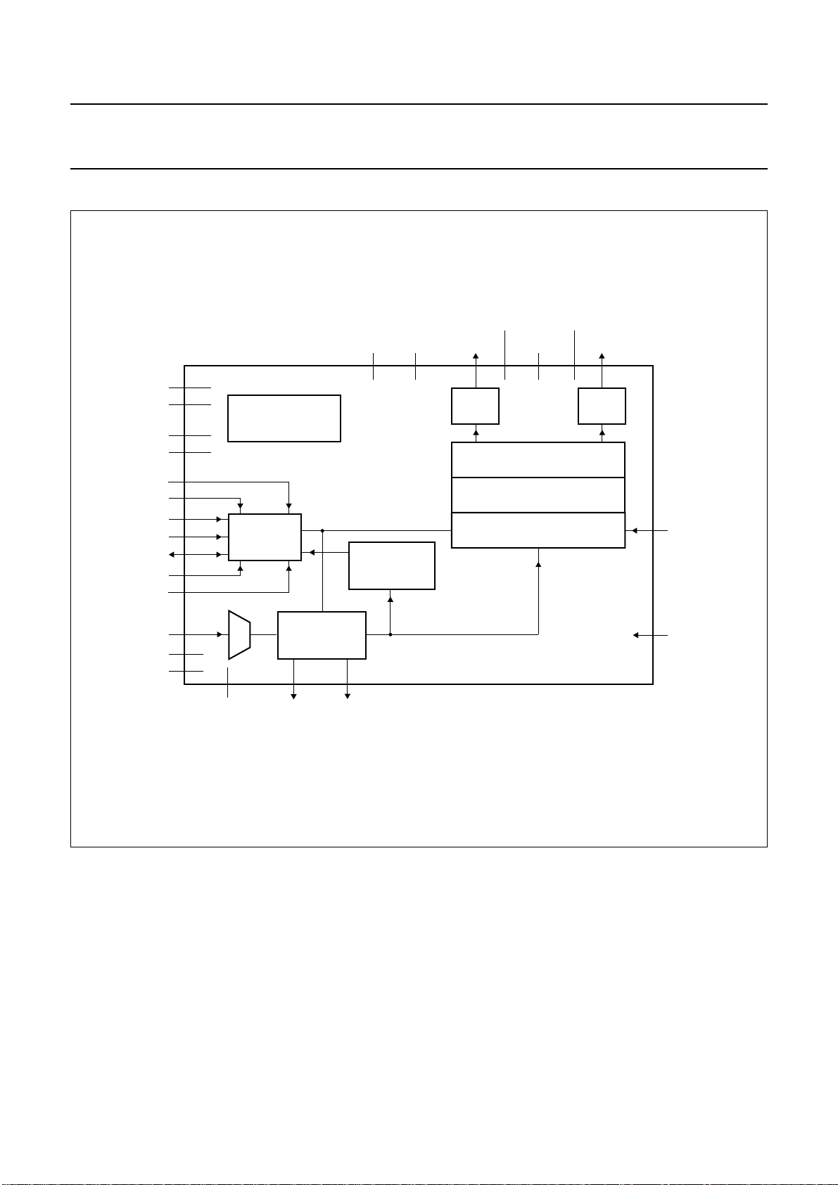
8 FUNCTIONAL DESCRIPTION
8.1 Clock regeneration and lock detection
The UDA1352TS contains an on-board PLL for
regenerating a system clock from the IEC 60958 input
bitstream.
Remark: If there is no input signal, the PLL generates a
minimum frequency and the output spectrum shifts
accordingly. Since the analog output does not have an
analog mute, this means noise that is out of band under
normal conditions can move into the audio band.
When the on-board clock locks to the incoming frequency,
the lock indicator bit is set and can be read via the L3-bus
or I2C-bus interface. Internally, the PLL lock indication can
be combined with the PCM status bit of the input data
stream and the status whether any burst preamble is
detected or not. By default, when both the IEC 60958
decoder and the on-board clock have locked to the
incoming signal and the input data stream is PCM data,
pin LOCKwillbeasserted.However,whenthe ICislocked
but the PCM status bit reports non-PCM data, pin LOCK is
returned to LOW level. This combination of the lock status
and the PCM detection can be overruled by the L3-bus or
I2C-bus register setting.
The lock indication output can be used, for example, for
muting purposes. The lock signal can be used to drive an
external analog muting circuit to prevent out of band noise
from becoming audible when the PLL runs at its minimum
frequency (e.g. when there is no SPDIF input signal).
TheUDA1352TShasa dedicated pin PCMDET toindicate
whether valid PCM data stream is detected or (supposed
to be) non-PCM data is detected.
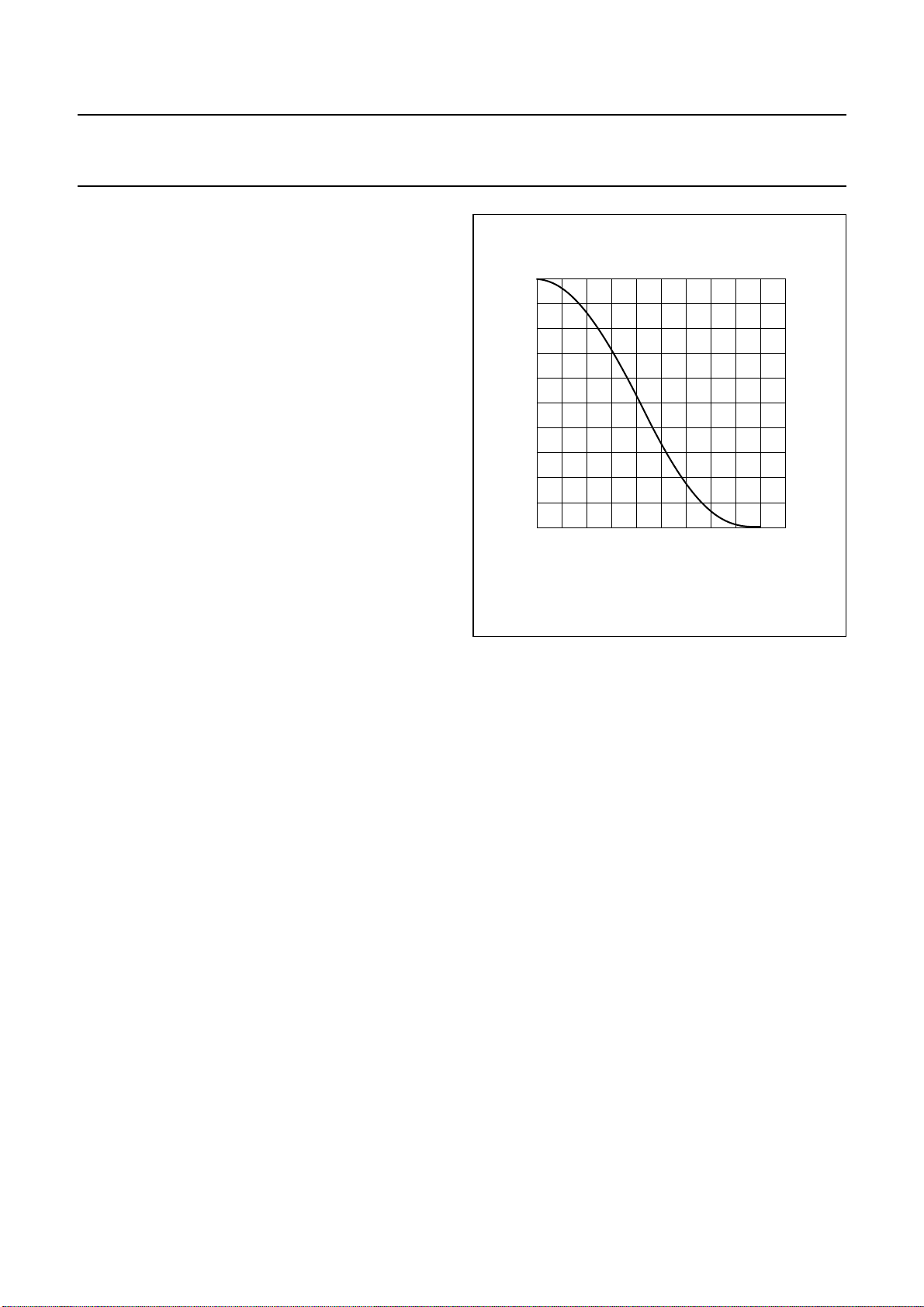
8.2 Mute
The UDA1352TS is equipped with a cosine roll-off mute in
the DSP data path of the DAC part. Muting the DAC (by
pin MUTE or via bit MT in the L3-bus or I2C-bus mode)
will result in a soft mute as shown in Fig.3. The cosine
roll-off soft mute takes 32 ×32 samples = 23 ms at
44.1 kHz sampling frequency.
When operating in the L3-bus or I2C-bus mode, the device
will mute on start-up. In the L3-bus or I2C-bus mode, it is
necessary to explicitly switch off the mute for audio output
by means of bit MT in the device register.
In the L3-bus or I2C-bus mode, pin MUTE will at all time
mute the output signal. This is in contrast to the UDA1350
and the UDA1351 in which pin MUTE in the L3-bus mode
does not have any function.
8.3 Auto mute
By default, the DAC outputs will be muted until the
UDA1352TS is locked, regardless of the level on
pin MUTEorthe stateofbit MT.In thisway,onlyvalid data
will be passed to the outputs. This mute is done in the
SPDIF interface and is a hard mute, not a cosine roll-off
mute.
If needed, this muting can be bypassed by setting
bit MUTEBP = 1 via the L3-bus or I2C-bus interface. As a
result, the UDA1352TS will no longer mute during
out-of-lock situations.
handbook, halfpage
01051525
1
0
0.8
MGU119
20
0.6
0.4
0.2
t (ms)
mute
factor
Fig.3 Mute as a function of raised cosine roll-off.