NXP Semiconductors i.MX RT Series User manual

1 Overview
This document focuses on the procedure of entering boundary scan mode for
board-level test. It provides the setup sequence and script examples to ensure
first-pass success.
Engineers should understand the standard for test access port and boundary
scan architecture from IEEE 1149.1.
1.1 Boundary Scan
Boundary scan is a method for testing interconnects on PCBs and internal IC
sub-blocks. It is defined in the IEEE 1149.1 standard.
In boundary scan test, each primary input and output signal on a device is supplemented with a multi-purpose memory element
called a boundary scan cell. These cells are connected to a shift register, which is referred to as the boundary scan register. This
register can be used to read and write port states.
In normal mode, these cells are transparent and the core is connected to the ports. In boundary scan mode, the core is isolated
from the ports and the port signals are controlled by the JTAG interface.
Figure 1 shows the principle of boundary scan chain.
Contents
1 Overview......................................... 1
1.1 Boundary Scan............................ 1
1.2 Test Access Port (TAP) JTAG..... 2
2 Installing software............................3
3 Hardware connection diagram........ 3
4 BSDL file validation using Lauterbach
JTAG debugger...............................8
5 Introduction to other EVK board of
i.MX RT series...............................13
6 Revision history.............................14
AN12919
Introduction to Boundary Scan of i.MX RT Series
Rev. 1 — March 2, 2021 Application Note

Figure 1. Boundary scan principle
1.2 Test Access Port (TAP) JTAG
The TAP is a general-purpose port and it can provide access to many test support functions built into the component. It has four
or five signals, as described in Table 1.
NXP Semiconductors
Overview
Introduction to Boundary Scan of i.MX RT Series, Rev. 1, March 2, 2021
Application Note 2 / 15

Table 1. JTAG pin signal description
Signal name I/O type Description
TCK Input The test clock input provides the clock for the test logic.
TMS Input The value of the signal present at TMS at the time of a rising edge at TCK
determines the next state of the TAP controller.
TDI Input Serial test instructions and data are received by the test logic.
TDO Output Serial output for test instructions and data from the test logic.
TRST_N Input Optional active low signal to reset the TAP controller.
2 Installing software
The TRACE32 installation package can be found on the Lauterbach page.
Download the
TRACE32_201909.7z
to the computer and install it.
1. Because the installation package is relatively large, you can install software components according to the target
processor to save hard disk space.
2. You can find installed driver at
C:\T32\bin\windows64\drivers
.
3 Hardware connection diagram
The TRACE32 debugger hardware always consists of:
• Universal debugger hardware
• Debug cable specific to the processor architecture
Figure 2 is a schematic diagram of hardware connection.
NXP Semiconductors
Installing software
Introduction to Boundary Scan of i.MX RT Series, Rev. 1, March 2, 2021
Application Note 3 / 15

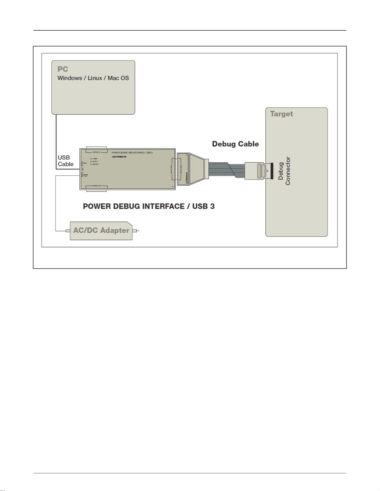
Figure 2. Schematic diagram of hardware connection
Suggestions for users include:
• To prevent the debuggers or target being damaged, it is forbidden to plug or unplug the debugger while target is powered on.
The recommended sequence for powering on or off is as follow:
— Power on: debugger >target
— Power off: target >debugger
• The debugger interface has pin1. Please double check the direction to prevent damages to the debugger or target.
• It is recommended to press F1 to enter the on-line help system to get familiar with debugger.
1. Taking RT1064 EVK board as an example, the hardware connection is as shown in Figure 3.
a. Connect Lauterbach JTAG debugger to the EVK board by the 20pin JTAG interface.
b. Connect to the PC through the USB cable, and then power on the debugger with a 5 V power adapter.
c. Connect the EVK USB port to the PC.
NXP Semiconductors
Hardware connection diagram
Introduction to Boundary Scan of i.MX RT Series, Rev. 1, March 2, 2021
Application Note 4 / 15

Figure 3. RT1064 EVK board hardware connection
2. Apply the NXP-MCUBootUtility-2.3.0 to burn one bit, 0x460 Boot Cfg1, in eFuse to enable JTAG. It can’t go back to SWD
after eFuse burn. Figure 4 shows the setup information.
NXP Semiconductors
Hardware connection diagram
Introduction to Boundary Scan of i.MX RT Series, Rev. 1, March 2, 2021
Application Note 5 / 15

Figure 4. NXP-MCUBootUtility-2.3.0 in eFuse to enable JTAG
3. Check the signals of three pins, TEST_MODE, GPIO_AD_B0_08, POR_B , according to the settings corresponding to
the COMPLIANCE_PATTERN part of the
BSDL
file. They should have the same status, 011, on the EVK board. Figure 5 is
compliance_patterns part of the
BSDL
file. Figure 6 shows test mode and the por_b connection.
Figure 5. COMPLIANCE_PATTERN PART OF BSDL FILE
NXP Semiconductors
Hardware connection diagram
Introduction to Boundary Scan of i.MX RT Series, Rev. 1, March 2, 2021
Application Note 6 / 15

Figure 6. Test mode and POR connection
4. The value of GPIO_AD_B0_08 is 1 in the
BSDL
file, but we pull down it to GND on the EVK board. So we should disconnect
the resistor R303 ground terminal, and pull up this pin with DCDC_3V3.
Figure 7. GPIO_AD_B0_08 connection
5. We used OPENSDA circuit on the RT1064 EVK board, which will affect the JTAG signal level during the Boundary
Scan test. So we should disconnect the SWD jump connectors, J47, J48, J49, and J50. Figure 8 shows SWD jump
connector disconnection.
NXP Semiconductors
Hardware connection diagram
Introduction to Boundary Scan of i.MX RT Series, Rev. 1, March 2, 2021
Application Note 7 / 15

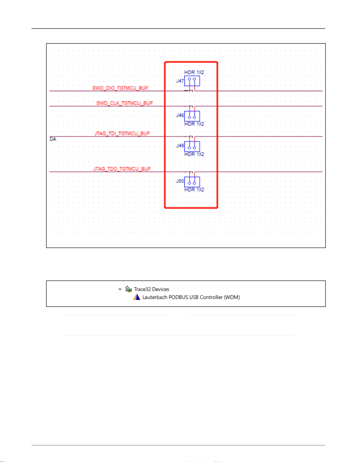
Figure 8. SWD jump connector disconnection
4 BSDL file validation using Lauterbach JTAG debugger
1. Trace32 Devices should appear in the Device Manager.
Lauterbach JTAG debugger recommended is LA-4533 Debug-USB3, with LA-7960/4513. Related information can
be found on the lauterbach page.
NOTE
2. Open the TRACE32 software and choose ARM32 USB.
NXP Semiconductors
BSDL file validation using Lauterbach JTAG debugger
Introduction to Boundary Scan of i.MX RT Series, Rev. 1, March 2, 2021
Application Note 8 / 15

3. Type in below commands, with each command followed by entering:
SYStem.Down
BSDL.RESet
BSDL.ParkState Select-DR-Scan
BSDL.state
4. BSDL.state window should now appear. Click the FILE button and load the BSDL file you want to validate. Figure 9 shows
the BSDL.state window.
Figure 9. BSDL.state window
5. After loading the file, type in command as below:
BSDL.SOFTRESET
6. Switch to the Check tab of the BSDL.state window. Click BYPASSall and IDCODEall button to see if both results can pass.
The BYPASS/CLAMP/HIGHZ check pass, as shown in Figure 10.
NXP Semiconductors
BSDL file validation using Lauterbach JTAG debugger
Introduction to Boundary Scan of i.MX RT Series, Rev. 1, March 2, 2021
Application Note 9 / 15

Figure 10. BYPASS and IDCODE check
7. Click the SAMPLEall button, and you will see No result becomes Test done. Double click the entity name, and the
BSDL.SET window appears, as shown in Figure 11.
Figure 11. SAMPLE check
8. In the BSDL.SET window, uncheck Intern to filter out the internal registers. The remaining contents are the sampled value
on each signal pins. Use a multimeter to measure voltage of at least three signal pins, and see if the logic state matches
the sampled value. SAMPLE check pass, Figure 12 shows BSDL.SET window.
NXP Semiconductors
BSDL file validation using Lauterbach JTAG debugger
Introduction to Boundary Scan of i.MX RT Series, Rev. 1, March 2, 2021
Application Note 10 / 15

Figure 12. BSDL.SET window
9. In the Instructions field, click EXTEST and in the DR mode field, choose Set Write as shown in Figure 13. Then switch to
the BSDL.state window and check SetAndRun and TwoStepDR, as shown in Figure 14.
Figure 13. BSDL.SET window EXTEST set up
NXP Semiconductors
BSDL file validation using Lauterbach JTAG debugger
Introduction to Boundary Scan of i.MX RT Series, Rev. 1, March 2, 2021
Application Note 11 / 15

Figure 14. BSDL.STATE window set up
10. Switch back to BSDL.SET window, click the buttons in the Enable column to enable output of corresponding signal pins
and click the buttons in “Reg.” column to toggle their output logic state 0 or 1. Use a multimeter to measure if the logic state
really toggles on those signal pins. At least three signal pins need to be verified. Then RELOAD/EXTEST check pass other
pins, as shown in Figure 15.
Figure 15. BSDL.SET window enable and toggle signal level
The following uses GPIO_AD_B0_14 as an example. It connects U1.H14 (RT1064 chip, as shown in Figure 16) and U12.1 (CAN
BUS chip, as shown in Figure 17) with the net name of CAN2_TX. When Reg. is set to 0, the corresponding level of above two pins
are 0 V. When Reg. is set to 1, the corresponding level of above two pins are 3.3 V.
NXP Semiconductors
BSDL file validation using Lauterbach JTAG debugger
Introduction to Boundary Scan of i.MX RT Series, Rev. 1, March 2, 2021
Application Note 12 / 15

Figure 16. The pin of RT1064 chip
Figure 17. The pin of CAN BUS chip
5 Introduction to other EVK board of i.MX RT series
For the boundary scan test, follow steps as below:
•RT1010-EVK board
1. Change to JTAG mode by burning eFuse.
2. Check the BSDL file to confirm the status of three pins in COMPLIANCE_PATTERN, as shown below:
(TEST_MODE, GPIO_AD_11, POR_B) (011)
Similar to RT1060-EVK, remove the pull-down resistor, R303, of the JTAG_MOD pin and connect it to the DCDC_3V3
power supply.
3. Ensure independent JTAG topology, avoid level interference of other multiplexed signals, and disconnect the
headers, J61, J62, J63, and J64.
4. Use the Lauterbach debugger to test. For details, see the introduction above.
•RT1020 includes two package types, LQFP144 and LQFP100, corresponding to two boards, RT1020-EVK and RT1020-
EVK100.
— RT1020-EVK board (LQFP144)
NXP Semiconductors
Introduction to other EVK board of i.MX RT series
Introduction to Boundary Scan of i.MX RT Series, Rev. 1, March 2, 2021
Application Note 13 / 15

1. Change to JTAG mode by burning eFuse.
2. Check the BSDL file to confirm the status of three pins in COMPLIANCE_PATTERN, shown as below:
(TEST_MODE, GPIO_AD_B0_02, POR_B) (011)
Similar to RT1060-EVK, remove the pull-down resistor, R57, of the JTAG_MOD pin, and connect it to the DCDC_3V3
power supply.
3. As the PMIC_ON_REQ signal will affect the boundary scan test, delete the R41 resistor and mount R39 with 100
K resistor.
4. Ensure independent JTAG topology, avoid level interference of other multiplexed signals, delete the R116
resistor, and disconnect the headers, J47, J48, J49, and J50.
5. Use the Lauterbach debugger to test. For details, see the introduction above.
— RT1020-EVK100 board (LQFP100)
1. Change to JTAG mode by burning eFuse.
2. Check the BSDL file to confirm the status of three pins in COMPLIANCE_PATTERN, shown as below:
(TEST_MODE, GPIO_AD_B0_02, POR_B) (011)
Similar to RT1060-EVK, remove the pull-down resistor, R41, of the JTAG_MOD pin, and connect it to the DCDC_3V3
power supply.
3. As the PMIC_ON_REQ signal will affect the boundary scan test, delete the R21 resistor and mount R16 with 100
K resistor.
4. Ensure independent JTAG topology, avoid level interference of other multiplexed signals, disconnect the
headers, J35, J36, J37, and J38.
5. Use the Lauterbach debugger to test. For details, see the introduction above.
•RT1170-EVK board
1. No need to change to JTAG mode by burning eFuse.
2. Check the BSDL file to confirm the status of three pins in COMPLIANCE_PATTERN, shown as below:
(TEST_MODE, GPIO_LPSR_13, POR_B, ONOFF) (0011)
Different from the RT1060-EVK, keep the pull-down resistor, R403, of the JTAG_MOD pin.
3. As the PMIC_ON_REQ signal will affect the boundary scan test, delete the R266 resistor and mount R421 with 100 K
resistor.
4. Ensure independent JTAG topology, avoid level interference of other multiplexed signals, delete the resistors R187,
R208, R195, R78, and disconnect the headers J6, J7, J8, and J9.
5. Use the Lauterbach debugger to test. For details, see the introduction above.
6 Revision history
Table 2. Revision history
Rev. Date Description
0 June, 2020 Initial release
1 March, 2021 Added Introduction to other EVK board of i.MX RT series
NXP Semiconductors
Revision history
Introduction to Boundary Scan of i.MX RT Series, Rev. 1, March 2, 2021
Application Note 14 / 15

How To Reach Us
Home Page:
nxp.com
Web Support:
nxp.com/support
Information in this document is provided solely to enable system and software implementers to use NXP products. There
are no express or implied copyright licenses granted hereunder to design or fabricate any integrated circuits based on the
information in this document. NXP reserves the right to make changes without further notice to any products herein.
NXP makes no warranty, representation, or guarantee regarding the suitability of its products for any particular purpose, nor
does NXP assume any liability arising out of the application or use of any product or circuit, and specifically disclaims any
and all liability, including without limitation consequential or incidental damages. “Typical” parameters that may be provided
in NXP data sheets and/or specifications can and do vary in different applications, and actual performance may vary over
time. All operating parameters, including “typicals,” must be validated for each customer application by customer's technical
experts. NXP does not convey any license under its patent rights nor the rights of others. NXP sells products pursuant to
standard terms and conditions of sale, which can be found at the following address: nxp.com/SalesTermsandConditions.
Right to make changes - NXP Semiconductors reserves the right to make changes to information published in this
document, including without limitation specifications and product descriptions, at any time and without notice. This
document supersedes and replaces all information supplied prior to the publication hereof.
Security — Customer understands that all NXP products may be subject to unidentified or documented vulnerabilities.
Customer is responsible for the design and operation of its applications and products throughout their lifecycles to reduce
the effect of these vulnerabilities on customer’s applications and products. Customer’s responsibility also extends to other
open and/or proprietary technologies supported by NXP products for use in customer’s applications. NXP accepts no
liability for any vulnerability. Customer should regularly check security updates from NXP and follow up appropriately.
Customer shall select products with security features that best meet rules, regulations, and standards of the intended
application and make the ultimate design decisions regarding its products and is solely responsible for compliance with all
legal, regulatory, and security related requirements concerning its products, regardless of any information or support that
may be provided by NXP. NXP has a Product Security Incident Response Team (PSIRT) (reachable at [email protected])
that manages the investigation, reporting, and solution release to security vulnerabilities of NXP products.
NXP, the NXP logo, NXP SECURE CONNECTIONS FOR A SMARTER WORLD, COOLFLUX,EMBRACE, GREENCHIP,
HITAG, ICODE, JCOP, LIFE, VIBES, MIFARE, MIFARE CLASSIC, MIFARE DESFire, MIFARE PLUS, MIFARE FLEX,
MANTIS, MIFARE ULTRALIGHT, MIFARE4MOBILE, MIGLO, NTAG, ROADLINK, SMARTLX, SMARTMX, STARPLUG,
TOPFET, TRENCHMOS, UCODE, Freescale, the Freescale logo, AltiVec, CodeWarrior, ColdFire, ColdFire+, the Energy
Efficient Solutions logo, Kinetis, Layerscape, MagniV, mobileGT, PEG, PowerQUICC, Processor Expert, QorIQ, QorIQ
Qonverge, SafeAssure, the SafeAssure logo, StarCore, Symphony, VortiQa, Vybrid, Airfast, BeeKit, BeeStack, CoreNet,
Flexis, MXC, Platform in a Package, QUICC Engine, Tower, TurboLink, EdgeScale, EdgeLock, eIQ, and Immersive3D are
trademarks of NXP B.V. All other product or service names are the property of their respective owners. AMBA, Arm, Arm7,
Arm7TDMI, Arm9, Arm11, Artisan, big.LITTLE, Cordio, CoreLink, CoreSight, Cortex, DesignStart, DynamIQ, Jazelle,
Keil, Mali, Mbed, Mbed Enabled, NEON, POP, RealView, SecurCore, Socrates, Thumb, TrustZone, ULINK, ULINK2,
ULINK-ME, ULINK-PLUS, ULINKpro, μVision, Versatile are trademarks or registered trademarks of Arm Limited (or its
subsidiaries) in the US and/or elsewhere. The related technology may be protected by any or all of patents, copyrights,
designs and trade secrets. All rights reserved. Oracle and Java are registered trademarks of Oracle and/or its affiliates. The
Power Architecture and Power.org word marks and the Power and Power.org logos and related marks are trademarks and
service marks licensed by Power.org.
© NXP B.V. 2020-2021. All rights reserved.
For more information, please visit: http://www.nxp.com
For sales office addresses, please send an email to: [email protected]
Date of release: March 2, 2021
Document identifier: AN12919
This manual suits for next models
1
Table of contents