Oakley Eurorack Modular Series User manual

Oakley Sound Systems
Eurorack Modular Series
Eight Step Sequencer
PCB Issue 1
Builder's Guide
1.2
Tony Allgood
Oakley Sound Systems
CARLISLE
United Kingdom

Introduction
This is the Project uilder's Guide for the issue 1 Sequencer module from Oakley Sound. This
document contains a basic introduction to the board set, a full parts list for the components needed
to populate the boards and some hints on how to build the unit.
For the User Manual, which contains an overview of the operation of the unit and the calibration
procedure, please visit the main project webpage at:
http://www.oakleysound.com/sequencer-e.htm
For general information regarding where to get parts and suggested part numbers please see my
useful Parts Guide at the project webpage or http://www.oakleysound.com/parts.pdf.
For general information on how to build my modules, including circuit board population, mounting
front panel components and making up board interconnects please see my generic Construction
Guide at the project webpage or http://www.oakleysound.com/construct.pdf.
2

The Sequencer PC set
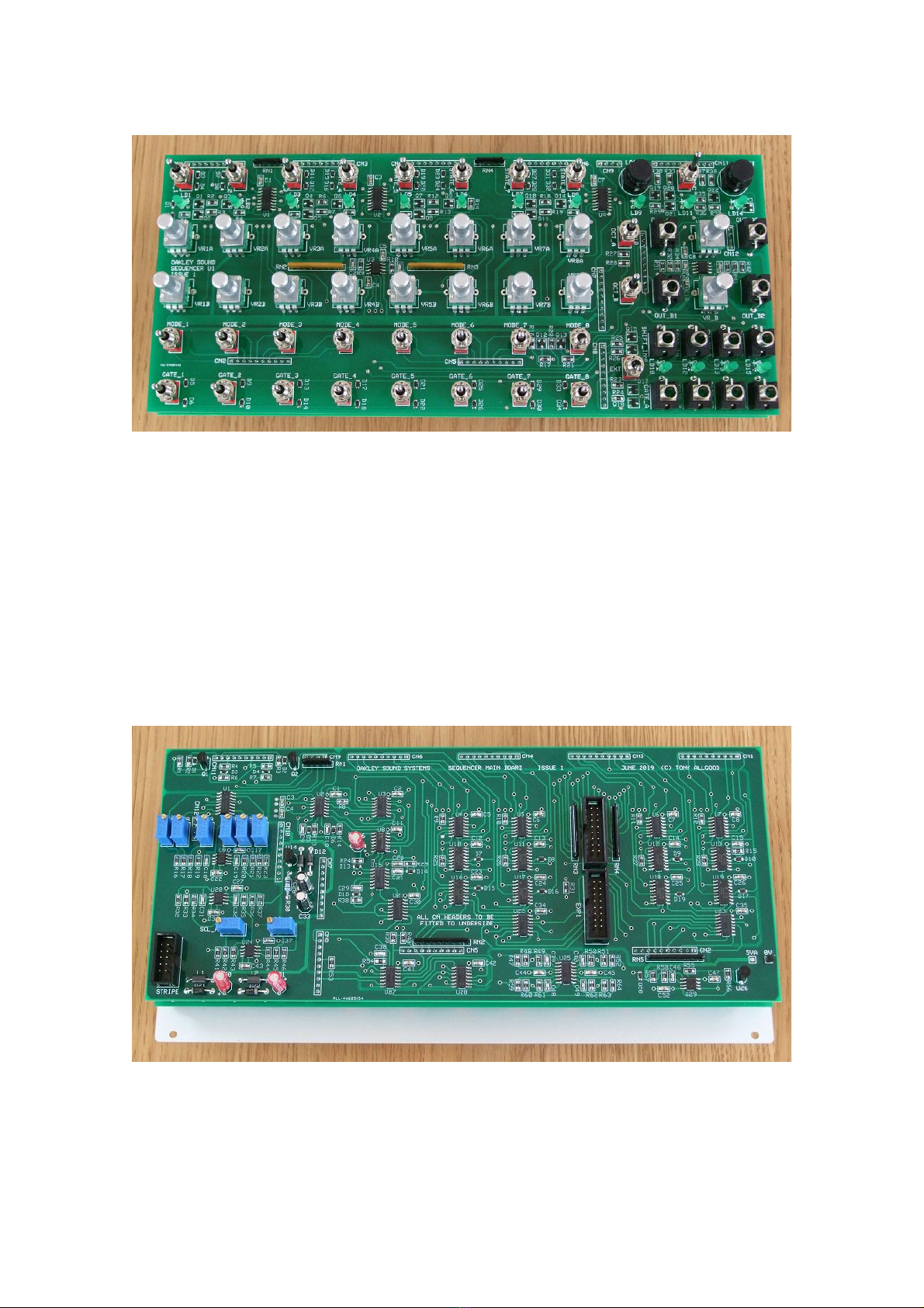
The issue 1 pot and switch board of the sequencer.
The electronics of the Oakley Sequencer is built on two printed circuit boards (PC s). The Pot and
Switch board hold the pots, switches, input and output sockets, LEDs, and the circuitry the controls
the LEDs and pots. All the front panel components are directly soldered to the Pot and Switch
board. The board is a double sided design meaning that there are electrically conductive copper
tracks on the top and bottom surfaces of the board. The surface mount components are all soldered
to the top side of the board.
The second board is called the main board. This holds the bulk of the sequencer circuitry, the
analogue output processing circuitry, the power supply conditioning, the +5V supply and the
precision +5V reference voltage used by the pot drivers on the Pot and Switch board.
The issue 1 Main Board fitted to the Pot and Switch Board and front panel.
The main board is a four layer design. This means that the board has layers of copper on top and
bottom sides, as well as two internal copper layers. The top internal layer is reserved for the two
3

main 0V connections used on the main board. The components, again a mixture of through hole and
surface mount devices, are soldered to the top of the board. However, because the boards used in
this project are fitted together so that their undersides face each other, the main board's components
are all accessible from the rear of the module. Although this means that you need to be a little
careful when handling the module, it does mean that fault finding is much easier than it would be if
the main board was facing the other way and no components would be visible.
The design requires plus and minus 12V supplies. The power supply should be adequately
regulated. The current consumption is around +85mA and -40mA. The 45mA difference between
the positive and negative rails is almost entirely due to the constant current LED drivers. The LED
driver circuits ensure that the module takes the same current whether the LEDs are on or off. This
reduces current spikes when the LEDs are turned on and off thus reducing unwanted noise on the
power supply lines in your modular.
The two boards are fitted back to back to allow easy access to all the components.
Power is routed onto the main board via the usual 10 way keyed IDC header. Reverse polarity
protection is provided by two Schottky diodes in series with the +12V and -12V lines. Internally the
Sequencer uses three 0V connections. One is used exclusively for the digital circuitry and LEDs,
another solely for the analogue circuitry like the pot drivers, and the third one for grounding the
front panel, ground lugs of the sockets and the pot's metalwork. These three 0V connections are
made using two pins each of the middle block of six pins on the 10 way power lead. It is imperative
therefore that any power supply distribution system connects all six middle pins of the ten way
power lead to the power supply's 0V (ground). This is the expected behaviour of any Eurorack
system but should the Sequencer not behave correctly be sure to check your power lead and power
distribution system first.
oth circuit boards are the same size, that is, 249 mm (wide) x 107 mm (high). The boards are
designed to go behind a panel that is 50HP wide.
4

Sequencer Parts Lists
The components are grouped into values, the order of the component names is of no particular
consequence.
Many of the parts for this circuit board are surface mount devices but not all of them. Take special
care when ordering your parts that you order the correct type of part. This parts list shows the type
of part needed whereas the circuit diagram does not.
A quick note on European part descriptions. R is shorthand for ohm. K is shorthand for kilo-ohm. R
is shorthand for ohm. So 22R is 22 ohm, 1K5 is 1,500 ohms or 1.5 kilohms. For capacitors: 1uF =
one microfarad = 1000nF = one thousand nanofarad. For electrolytic capacitors the maximum
working voltage is normally given with the value, eg. 1uF/63V is a one microfarad capacitor with a
working DC voltage of 63V.
To prevent loss of the small ‘.’ as the decimal point, a convention of inserting the unit in its place is
used. eg. 4R7 is a 4.7 ohm, 4K7 is a 4700 ohm resistor, 6n8 is a 6.8 nF capacitor.
Sequencer Main oard issue 1
Resistors
All single resistors except R30 are surface mount, size 0805 (or metric 2012) 1% 125mW metal
film.
120R R57
220R R51, R32, R48, R60, R63, R37
2K2 R31
3K3 R64, R50, R62, R52, R49, R61, R59, R47
10K R56
18K R7, R6
22K R54, R36, R35, R29, R38, R14, R34, R33, R58, R55, R13
39K R19, R20
47K R1, R8
62K R23, R16
82K R4, R5
97K6 R42, R45
100K R3, R12, R27, R11, R10, R25, R46, R2, R26, R44, R24, R41, R43, R15, R28, R9,
R40, R53, R39
130K R17, R22, R21, R18
47R, 1/4W through hole metal film R30
100K x 4 5-pin bussed* resistor network RN1
100K x 8 9-pin bussed* resistor network RN2, RN3, RN4, RN5
* A bussed or commoned resistor network is a single component that contains a number of 2%
resistors connected together. The commoned pin is labelled with a dot and must be put into the
board so that the dot lines up with the square pad on the PC .
5

Capacitors
The following capacitors are surface mount, size 0805 (or metric 2012) multilayer ceramic,
dielectric C0G (or NP0), working voltage 50V, tolerance +/-5%.
33pF C18, C19
47pF C31, C32
100pF C39, C48, C49, C46, C40
1nF C9, C21, C29, C10, C38
The following capacitors are surface mount, size 0805 (or metric 2012) multilayer ceramic,
dielectric X7R, working voltage 50V, tolerance +/-5%.
100nF C1, C12, C14, C42, C30, C3, C4, C20, C2, C5, C35, C7, C11, C15, C24, C26, C8,
C6, C23, C41, C34, C25, C13, C22, C44, C45, C47, C43, C37, C17, C36, C52, C27
The following capacitors are standard through hole electrolytic capacitors with 0.1” (2.5mm) or
0.2” (5mm) radial leads.
1uF/63V electrolytic C16
4u7/63V electrolytic C50, C51
10uF/35V electrolytic C33
47uF/25V electrolytic C28
Discrete Semiconductors
The following devices are surface mount parts.
1N4148WS signal diode D1, D17, D20, D3, D8, D10, D16, D13, D2, D9, D15, D7, D4, D19
AT42WS Schottky diode D5, D14, D6, D18
The following devices are standard through hole parts.
1N4001 diode D11
1N5819 Schottky diode D12, D22, D21
C550 NPN transistor Q1, Q2
Integrated Circuits
The following parts are all surface mount devices. All are small outline (SOIC) narrow body
packages.
74HC00D quad NAND gate U8
74HC02D quad NOR gate U22, U28, U3, U23
74HC14D hex schmitt trigger U27, U2, U15
74HC74D dual d-type flip-flop U5, U21, U7, U4, U6
74HC4053D analogue switch U12, U18, U19, U13, U16, U10, U17, U11
DG202 DY analogue switch U1
6

TL072ACD dual op-amp U20, U24, U29
AD712JRZ dual op-amp U9
TL074CDR quad op-amp U25
The following devices are standard through hole parts.
78L05 +5V regulator U14
LM4040-5.0V 5V reference U26
Trimmers (preset) resistors
The multiturn trimmers are ourns 3296W, Vishay T93YA or similar.
10K multiturn trimmer T1A, T2A, T3A, T1 , T2 , T3
5K multiturn trimmer SCL_A, SCL_
Miscellaneous
Leaded ferrite bead L1, L2
2 x 5 0.1” boxed header STRIPE
2 x 8 0.1” boxed header EXP1, EXP2
4 way 0.1” SIL socket CN9, CN12
10 way 0.1” SIL socket CN1, CN2, CN3, CN4, CN5, CN6, CN7, CN8, CN10, CN11
CN1 to CN12 are mounted on the underside of the board, facing down, and soldered from the top.
Special care must to be taken to ensure that these connectors are mounted perpendicular to the
board surface.
7

Sequencer Pot & Switch oard issue 1
Resistors
All single resistors are surface mount, size 0805 (or metric 2012) 1% 125mW metal film.
120R R19, R36, R20, R35, R7, R16, R13, R3
220R R34, R40
470R R21, R15, R17, R11, R1, R39, R29, R5
10K R37
12K R31, R42
51K R9, R10
100K R6, R8, R4, R32, R41, R2, R38, R26, R23, R24, R25, R33, R22, R30, R12,
R14, R27, R28, R18
100K x 4 5-pin bussed* resistor network RN1, RN4
220K x 8 9-pin bussed* resistor network RN2, RN3
* A bussed or commoned resistor network is a single component that contains a number of 2%
resistors connected together. The commoned pin is labelled with a dot and must be put into the
board so that the dot lines up with the square pad on the PC .
Capacitors
The following capacitors are surface mount, size 0805 (or metric 2012) multilayer ceramic,
dielectric C0G (or NP0), working voltage 50V, tolerance +/-5%.
47pF C6, C11, C9, C2
The following capacitors are surface mount, size 0805 (or metric 2012) multilayer ceramic,
dielectric X7R, working voltage 50V, tolerance +/-5%.
100nF C8, C7, C3, C10, C5, C4, C1
Discrete Semiconductors
The following devices are surface mount parts.
1N4148WS signal diode D1 – D34
C850 NPN transistor Q19, Q20, Q10, Q17, Q16, Q15, Q7, Q4, Q6, Q9, Q23, Q14, Q3, Q1,
Q18
C860 PNP transistor Q2, Q8, Q13, Q22, Q11, Q12, Q5, Q21
8

The following devices are standard through hole parts.
3mm green LED LD1 – LD15
See later in this document for details regarding the fitting of the LEDs.
Integrated Circuits
The following parts are all surface mount devices. All are small outline (SOIC) narrow body
packages.
CD4049U D hex inverter U1, U2, U4
AD712JRZ dual op-amp U3
TL072ACD dual op-amp U5
Potentiometers
All pots are Alpha 9mm vertical pots with 6.35mm round shafts.
50K linear 9mm VR_A, VR_ , VR1A – VR8A, VR1 – VR8
Switches
C&K D6R push switch SHIFT, LOAD
On-Off-On toggle switch GATE_1 – GATE_8, STATE_1 – STATE_8, MODE_1 – MODE_7,
OCT_A, OCT_
On-On toggle switch SYNC, EXT, MODE_8
Miscellaneous
4 way 0.1” SIL header* CN9, CN12
10 way 0.1” SIL header* CN1, CN2, CN3, CN4, CN5, CN6, CN7, CN8, CN10, CN11
* SIL headers fitted to the underside of the board and soldered from the top. ie. the pins face down.
Thonkiconn 3.5mm socket OUT_A1, OUT_A2, OUT_ 1, OUT_ 2, CV_IN_A, CV_IN_ ,
RESET, GATE_A, GATE_ , GATE_A , SHIFT_IN, LOAD_IN
18 knobs to suit. Davies 1900H or clones thereof are to be recommended.
9

Part Sourcing
For general information regarding where to get parts and suggested part numbers for Oakley
projects please see my Parts Guide at the project webpage or www.oakleysound.com/parts.pdf.
The front panel is obtained either from Schaeffer in Germany, or Front Panel Express (FPE) in the
US. The database for the panel is provided on the project webpage and this file can be opened,
edited and ordered using the Frontplatten Designer program available free from Schaeffer or FPE.
The cost of the 50HP wide panel was around 55Euros at the time of writing. The panel is 2.5mm
thick and has a natural silvery finish. The black text is printed, although it is possible to edit the
database to have the text engraved.
The pots are Alpha 9mm vertical pots as sold by Thonk and others. I use Thonk's standard ones
with 6.35mm (0.25”) round shafts. Other shaft types are available, like splined or D-type, and you
should purchase those that are compatible with your choice of control knob. I prefer the round
shafts as they require control knobs that have a fixing screw. Although these knobs take more time
to place and secure, the height at which the knob sits on the pot shaft is under your control. Push fit
knobs can sometimes not sit at the right height which is unsightly if they are too high, or graunch
against the pot's securing nut and washer if they are too low.
For control knobs I use Davies 1900H clones available from Thonk and others.
The two C&K D6R tactile switches are available from Thonk as their 'C&K Tactile switch'. You
can get them in different colours but I prefer black.
The toggle switches are a standard sub-miniature type that are designed to fit directly into a PC .
The three way on-off-off ones are available from Thonk as their DW2 sub-miniature switch. The
two on-on switch is available from Thonk as their DW1 sub-miniature switch. oth the DW1 and
DW2 switches are made by Dailywell and offer good performance for their price.
All of the 3.5mm sockets are the same type and are available from Thonk known either by their
Thonkiconn moniker or as part number PJ398SM.
The fixed 2.54mm (0.1”) interconnects are in two parts, the male header, and the female socket or
receptacle. I use both ten way and four way single in line (SIL) connectors in the Sequencer. The
ones I use are made by Multicomp, although more expensive types are available which may offer
increased longevity. These are the Multicomp part numbers for the parts I used:
10 way socket 2212S-10SG-85
10 way header 2211S-10G
4 way socket 2212S-04SG-85
4 way header 2211S-04G
You can carefully cut the ten way header to give you two four way headers. It is not possible,
however, to cut down the ten way socket to smaller sizes.
The 3mm light emitting diodes (LED) are green in my prototype. However, you can chose any
colour you wish so long as the LED's forward voltage (Vf) does not exceed 2.5V. Red, yellow, and
orange should work fine. I chose to use flat topped 'cylindrical' LEDs so that the flat top of the LED
10

lies in the same plane as the front of the panel. Standard dome topped LEDs would work just as
well. Standard diffused LEDs are to be recommended as they can be seen more clearly from an
angle. The green ones I use are Mouser part number 859-LTL-2231AT, or Farnell part number
1142496.
For resistor networks RN2 and RN3 on the Pot and Switch board if you can get the 220K network
in 1% tolerance then this is to be preferred. However, most suppliers only have 2% types in stock.
Using 1% networks will make the ranges of the individual step pots more closely matched but 2%
networks will give acceptable performance.
All the dual op-amps, with the exception of U3 on the Pot and Switch board and U9 on the Main
oard, are recommended to be TL072ACD. Note the A in the part number suffix, this is the
improved specification version of the standard TL072 which has lower offset voltages. Offset
voltage is an unwanted voltage on the inputs of an op-amp which then manifests itself as an error
voltage on the output of the op-amp. For example, if all the pots on the sequencer were at their
minimum one might expect the output of the sequencer to be exactly 0V. However, because of
offset voltages in the various op-amps in the signal chain, it is likely to be something between
+5mV and -5mV. Using a standard TL072 would give appreciably higher offset voltages than this
which may cause noticeable pitch discrepancies.
U3 on the Pot and Switch board and U9 on the Main oard are both AD712JRZ. (Mouser part
number 584-AD712JRZ, Farnell part number 9426400.) This is a dual precision FET op-amp and is
somewhat more expensive than the TL072ACD. However, the AD712JRZ has a very low offset
voltage and since U3 and U9 form important parts of the CV signal chain it is useful to make these
parts as accurate as possible. It is possible to use a TL072ACD in these two locations should the
additional expense prove to be too much. However, if you can, then U3 should be a AD712JRZ at
the very least.
Schaeffer's panels allow text and simple raphics to be either printed or en raved. Printin is enerally cheaper
on bi er panels but the text is not so well defined as from their en ravin service.
11

Populating the Circuit oards
For general information on how to build Oakley modules, including circuit board population,
mounting front panel components and making up board interconnects please see my generic
Construction Guide at the project webpage or http://www.oakleysound.com/construct.pdf.
Main Board Construction
All the surface mount components should be soldered first. Take care to treat all semiconductors as
static sensitive devices even when they have been soldered to the board. Later, once the board is
complete and the resistor packs are soldered into place, the board will be more resilient to static
discharge.
The next items to be soldered are the single in line (SIL) sockets. These are to be fitted to the
underside of the board and soldered from the top side.
Special care should be taken to ensure that each SIL socket sits at right angles to the board surface.
One way to do this is to temporarily fit the SIL headers into the SIL sockets and slide the Main
board and Pot and Switch board together with the headers and sockets in between. Then solder the
headers to the main board. Pulling the two boards apart should reveal all the sockets neatly in place
and at the correct angle.
The next items to be soldered will be the through hole components. If you are water washing your
board do this before fitting the eight trimmers as these devices are cannot be immersed in water.
Take special care with the resistor networks to ensure that the dot or line on the package lines up
with the square pad on the circuit board. You should also make sure that the three boxed headers are
correctly orientated. Pin 1 is normally designated with a little arrow shape on the plastic housing of
12

the header and this should align with the square pad on the board. Also, the hole in the housing
should correspond to the little box shape on the board's legend.
The power supply inlet, a 10 way (2 x 5) IDC boxed header. Note the orientation of the notch in the side of the
plastic housin .
You should also fill the two holes, marked 0V and 5VA, in the bottom right corner of the Main
oard with a bit of solder. Or, make a handy ground tag by soldering a spare header pin in the 0V
hole.
The 0V hole makes a handy round reference point for scope probes and voltmeters.
13

Pot and Switch Board Construction
The surface mount parts should be soldered first. Take care to treat all semiconductors, especially
the 4049U devices, as static sensitive devices even when they have been soldered to the board.
Once the board is complete and the resistor packs are soldered into place, the board will be more
resilient to static discharge.
Now solder the four resistor networks into place. These are mounted on the top of the board and
soldered from the underside. Fit the SIL headers into place from the underside of the board and
solder from the top of the board. It may be worth temporarily fitting the Pot and Switch board to the
Main oard so as to hold the headers exactly at right angles while you solder.
The remaining parts are the front panel components and to fit these properly you should have your
front panel ready. The panel will be used as a jig to hold the parts in the correct place while you
solder. Failure to use the panel as a jig for these components will almost certainly mean that the
panel will not slide onto the components.
The first parts to place, but not solder will be the pots. Issue 1 of the Pot and Switch board has the
two securing lugs' holes for the pots a little further apart than perhaps they should be. As such, the
pots should be fitted so that the three pot pins go into the board first and then ease in the two lugs
into their holes. The pot should then be firmly pushed into the board which will splay the lugs
slightly apart. The pot should then be held quite firmly in the board. Do this for all the pots. Do not
solder any of the pots at this point.
2.54mm (0.1”) SIL headers fitted to the underside of a completed Pot and Switch Board.
With the board on a horizontal surface and facing upward fit all the toggle switches and sockets. Do
not fit the LEDs, nor push switches yet. Ensure that the three on-on switches go in the correct
places. Place one of the toothed washers that came with the switches onto each switch.
Now ease the panel down onto the components making sure that all their threads are sitting snugly
in their holes. Place a washer and a nut on each of the two step 1 pots, and each of the two CV
output pots. Tighten the nuts but not too tightly. This should hold the panel in place so that you can
turn the module over to reveal the underside of the circuit board. The switches will rattle about but
should not fall out. Now solder all the pots.
14

Turn the board around so that the front of the module is facing you. Fit a suitable washer and nut on
each socket. Gently twist, but do not tighten, each nut into place and solder each socket from the
underside.
Do the same for all the toggle switches. Gently affix the securing nut onto each switch. As you turn
the nut on each switch the switch will be pulled up towards the panel so that it sits slightly off the
board. The switch lugs, however, are long enough to still stick out from the underside of the board
where they can now be soldered.
The front panel is almost complete but for the LEDs and push switches. I'll not hide the fact that
this next bit is really quite fiddly. ut we're nearly there so let's push on. Remove all the nuts and
pull the panel away from the board. Keep the board upright so that the washers do not fall off the
switch threads. Fit, but not solder, the push switches into place and ensure that the flattened edge of
the switch aligns with the pattern on the circuit board. Fit the panel back over the pots, easing the
panel over the newly fitted push switches and temporarily secure the panel using a couple of pot
nuts. Now solder the two push switches into place. You will need to push down on each switch
from the front as you solder to make sure they are flat against the top surface of the circuit board.
Once done, check that each switch moves smoothly in its hole.
A close up on the socket field. Note the toothed washers on the to le switches.
Now take the panel off again. It's time to finally fit the LEDs. LEDs do not light if they are not
fitted the correct way around so it is imperative that you do this bit right. The cathode of the LED
goes into the square pad, that is, the one on the right with the board facing you. Once again we are
15

fitting the devices into place but are not soldering them just yet. Ease the panel back on, taking care
that the push switches are not squashed underneath. Fit a couple of pot nuts to hold the panel in
place. Now tease each LED through its panel hole by using its leads that are sticking out the bottom
of the board.
If you are using standard dome topped LEDs then simply push them into the hole as far as they will
go and solder each one in turn. If you are using flat topped LEDs then you may wish to have them
align with the top surface of the panel. This is not a trivial task but one way is to use a bit of sticky
tape over the holes and let the LEDs push up against that before soldering each one in turn.
The grip of the multiple SIL interconnects are strong enough to hold the two boards together for
most uses. Should you require more rigidity then a small blob of silicone sealant or heat melt glue
across the join between the plastic housings of CN1, CN8 and CN11 would hold everything
together tightly. However, it is best not to do this until your unit has been thoroughly tested.
16

Testing
It is prudent to test the main board before fitting it to the pot and switch board. If you have a bench
power supply that allows you to select the current limit then set both the +12V and -12V supplies to
a current limit of 100mA. This should prevent any serious meltdowns if there is a problem with the
build.
Power up the main board on its own. If you can measure power supply current then it should be
around -30mA and +35mA. Anything significantly more than this will indicate a problem. If you
can't measure current then check that no devices are getting warm.
With a voltmeter measure the voltage between the 0V and 5VA pads in the right hand bottom
corner of the board. It should read somewhere between 4.9V and 5.1V. This is the analogue +5V
supply.
Now measure the voltage between the 0V pad and the anode of D11. This is the top lead of the
diode next to the text 'U14'. The voltage should be between 4.9V and 5.1V. This is the digital +5V
supply.
Now measure the voltage between the 0V pad and the top lead of the through hole resistor R30. It
should measure somewhere between 11.0 and 11.5V. If it is significantly less than this the current
being taken from the digital parts of the circuitry is too great and there is a fault.
If all is well, then the main board can be powered down. Wait a couple of minutes and then attach
the main board to the pot and switch board. e very careful to ensure all the SIL connections are
correctly in place.
Initialising
Set up the Sequencer module with the following settings:
All individual step load switches to 'Load Off', except step 1 which should be set to 'Load On'.
All the step mode switches should be set to the middle 'normal' position, except step 9 which should
be in the 'reset' position.
All the gate select switches should be in their central position.
The two scale switches should both be set to X4.
The 'Load on Shift' switch should be off, ie. in the up position.
The 'Gate Width' switch should be in the 'Full' position.
The pot positions are not important at this stage.
Now power up again. If you can monitor the current taken by the module then it should be around
-40mA and +85mA. The only LEDs that should be lit are the step 1 LED and probably the Reset
Out LED.
17

Shift Register Test
Push the 'Shift' button and the step 1 LED, and the Reset LED, if it was on, should now go out and
the step 2 LED should go on. Repeatedly pressing shift will cause the lit LED to move along the
steps and then return back to the beginning. The reset LED should also light when the sequencer
returns back to step 1. The LED below the shift button should light each time you press the shift
button and will stay lit for as long as you hold the button.
Now set the step mode switch on step 4 to reset. Push shift several times to see that the sequencer
now resets after just four steps, and does not proceed onto step 5. You may now wish to check each
step mode switch works in the same manner. Note that setting step 1's mode switch to reset will
make the sequencer stay on step 1.
Skip Mode Test
Put all the step mode switches back into the normal position and press the shift button enough times
to light step 1's LED again. Now set step 1's mode switch to skip. Press the shift button to advance
the sequence but this time when it gets to the end it should now restart at step 2 and miss step 1
entirely. That is, step 1 is skipped. Now check the skip function works for all the steps. Note that
the skip function is only enabled the next time that step is invoked. You cannot force a step to skip
while it is active. Note also the reset LED, this should only light when the sequencer is reset back to
the first available (non skipped) step.
Gate Output Test
Put all the step mode switches back into the normal position and press the shift button enough times
to light step 1's LED again. Now set step 1's gate switch to A. You should notice that both the Gate
A and A+ LEDs turn on. Now flip the switch to . The Gate and A+ LEDs should now be on.
Check that all the steps have correctly working gate switches by using the shift button to advance
the sequence from step 1 through to step 8.
Now set all step gate switches to A. The Gate A and A+ LEDs should remain on whichever step is
active. Set the 'Gate Width' switch to 'shift' and the two gate output LEDs should turn off. Press the
shift button again and you should notice that the gate output LEDs light up for as long as you are
holding down the shift button.
Parallel Load Test
Set all the switches back to how they were in the initialising stage. Set step 1's load switch to 'load
off'. Press the 'load' button and all step LEDs should be off. Notice that pressing the load button
should cause the load LED to light and the 'Pre-load' LED to toggle on and off with each press.
Now set all the step load switches to 'load on'. Press the load button and all the step LEDs should
turn on. Now set all the step load switches to 'load off' again. Press the load button and all the step
LEDs should turn off.
Set only step 1 and step 5 load switches to 'load on'. Hit load and just step 1 and step 5 should be
active. Advance the sequence with the shift button and check that you now have two LEDs moving
along.
18

Pressing load at any point in the sequence will force the Sequencer back to a state given by the load
switches, ie. in this case, step 1 and step 5 will be active.
Set the 'Load on Shift' to its down position which will turn this function on. Pressing load now
should still light the pre-load LED but the active step LEDs should not change. Pressing shift now
will do two things, turn off the pre-load LED and turn on the chosen steps of 1 and 5. In other
words, in this mode, pressing load arms the sequencer so that it will only load on the next shift
command.
C Outputs
The CV outputs should be calibrated before the unit is to be used properly and full calibration
details are to be found in the User Manual. However, it is worthwhile to check that the CV outputs
are working correctly before you install the Sequencer into your modular.
Once again set all the switches back to how they were in the initialising stage. Press load to set step
1 active. Insert a patch lead into the 'CV Out A1' output socket and measure the voltage between the
tip and sleeve connections at the free end of the patch lead. Rotate the top pot on step 1 to its
minimum value. Check that the voltage is very close to 0.000V (+/-10mV). Now move the pot to its
maximum value. Check that the voltage is approximately +4V. It doesn't have to be precisely
4.000V as this will be adjusted during the calibration process. Set the scale switch to X2 and the
voltage should fall to roughly 2V. Set the scale switch to X1 and the voltage should fall to around
1V.
Repeat the same procedure with the CV Out 1 output using the lower pot on step 1.
Now insert the patch lead into CV Out A2. Keeping step 1's pot at its maximum value measure the
voltage of CV Out A2. The voltage should be positive and with the pot just to the left of the socket
you should be able to adjust the voltage from 0.00V to around +9.5V.
Repeat the above procedure with the CV Out 2 output and its pot.
19

Final Comments
If you have any problems with building the module, an excellent source of support is the Oakley
Sound Forum at Muffwiggler.com. I am on this group, as well as many other users and builders of
Oakley modules.
If you can't get your project to work and you are in the EU, then Oakley Sound Systems are able to
offer a 'get you working' service. If you wish to take up this service please e-mail me, Tony
Allgood, at my contact e-mail address found on the website. I can service either fully populated
PC s or whole modules. You will be charged for all postage costs, any parts used and my time at
25G P per hour. Most faults can be found and fixed within one hour, and I normally return
modules within a week. The minimum charge is 25G P plus return postage costs.
If you have a comment about this builder's guide, or have a found a mistake in it, then please do let
me know. ut please do not contact me directly with questions about sourcing components or
general fault finding. Honestly, I would love to help but I do not have the time to help everyone
individually by e-mail.
Last but not least, can I say a big thank you to all of you who helped and inspired me. Thanks
especially to all the great people on the Synth-diy and Analogue Heaven mailing lists and those at
Muffwiggler.com.
Tony Allgood at Oakley Sound
Cumbria, UK
© June 2019
20
Table of contents
Other Oakley Recording Equipment manuals