TX-SV515PRO
Oo oO
Ref.
No.3449
MODEL
TX-SV515PRO/
II
Black
model
BHMD,
BHMDN,
BHMDC
120V
AC,
60Hz
BHMP
230V
AC,
50Hz
BHMW
op
120/220V
AC,
50/60Hz
BHMQA
240V
AC,
50Hz
SAFETY-RELATED
COMPONENT
WARNING!
TABLE
OF
CONTENTS
COMPONENTS
INDENTIFIED
BY
MARK
AON
THE
SCHEMATIC
DIAGRAM
AND
IN
THE
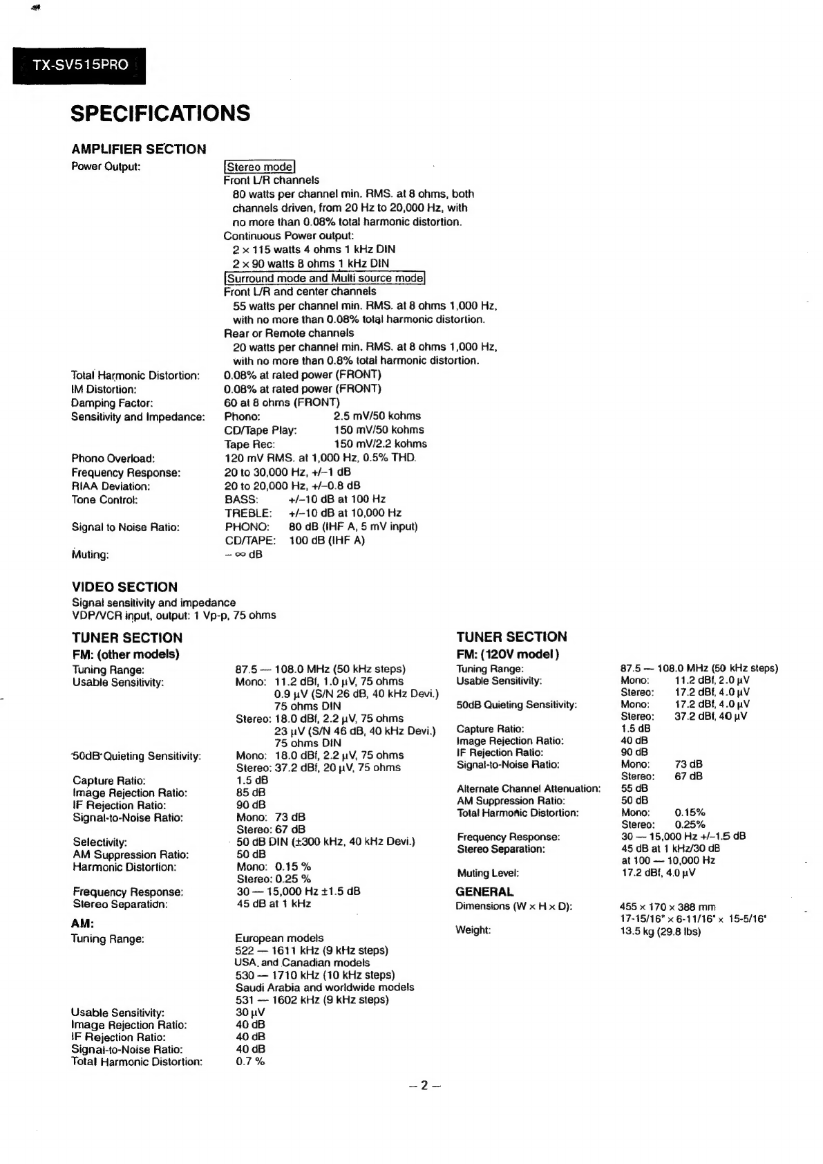
Specifications..........ccscsscccseesesseesenceeeesesseseeateensenensennecneneneneneees
2
PARTS
LIST
ARE
CRITICAL
FOR
RISK
OF
FIRE
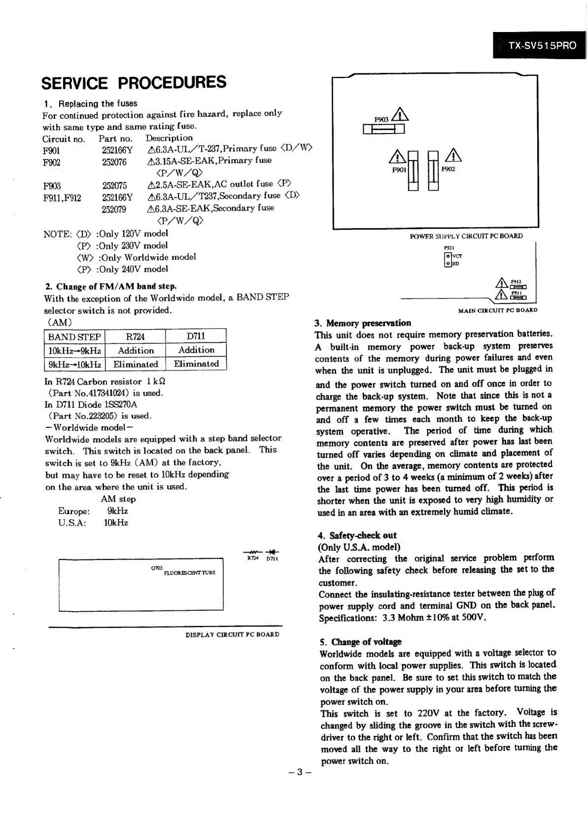
Service
procedures
AND
ELECTRIC
SHOCK.
REPLACE
THESE
Exploded
view
COMPONENTS
WITH
ONKYO
PARTS
WHOSE
Parts
list..........-
:
PART
NUMBERS
APPEAR
AS
SHOWN
IN
THIS
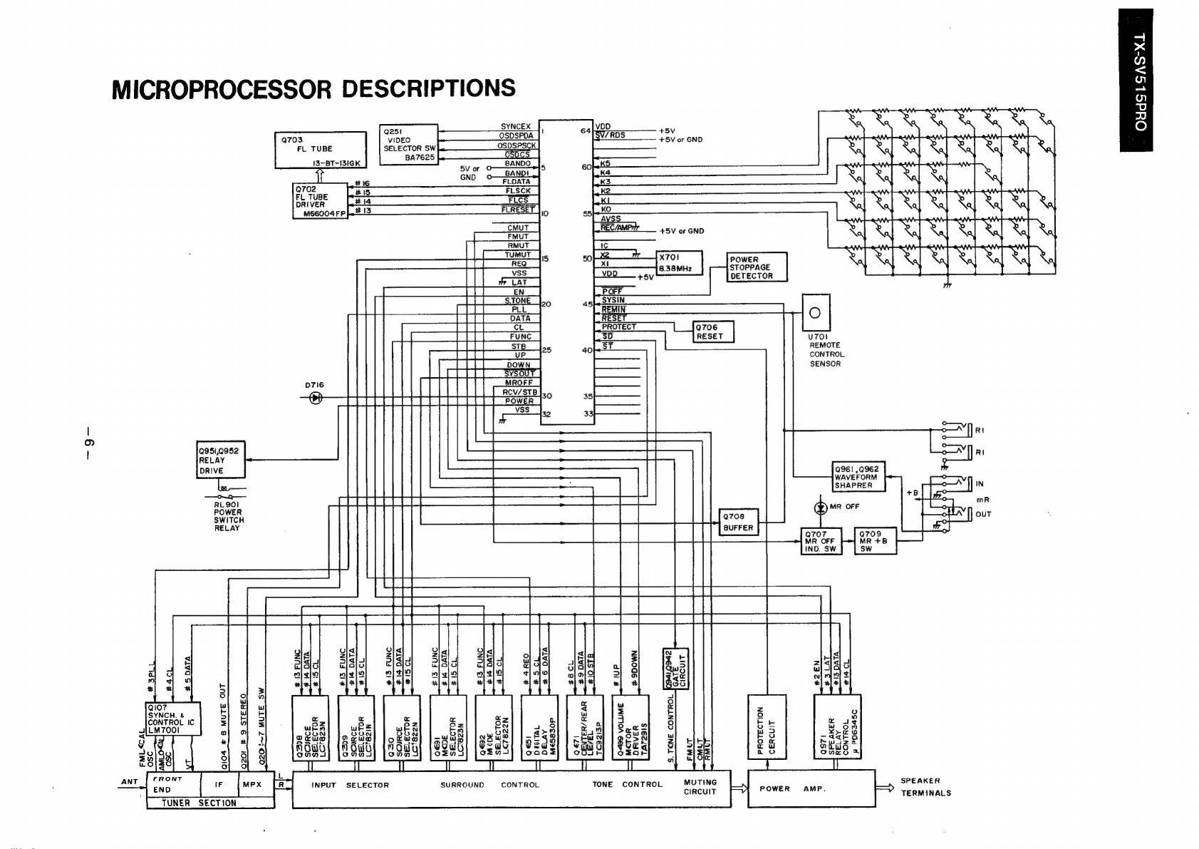
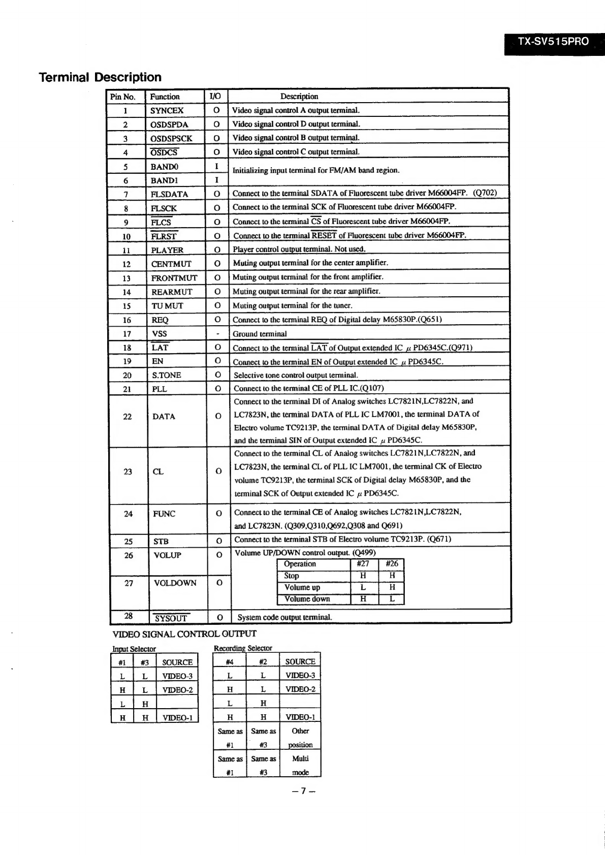
Microprocessor
GeSCriptiONs..............:cceseecesreseereeressrerestsnenessnennes
6
MANUAL.
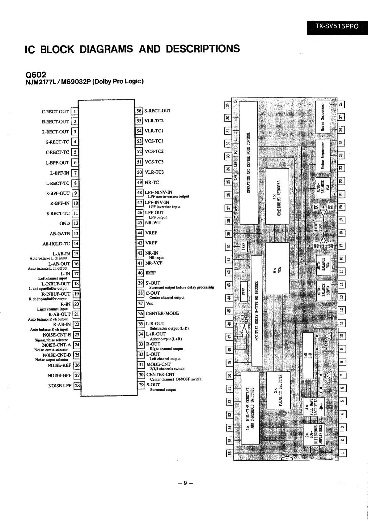
IC
block
diagrams
and
eSCTIPtIONS............---ecseseseerecereeneeetnenseen
ees
9
MAKE
LEAKAGE-CURRENT
OR
RESISTANCE
Block
diagram..........ccccccceceeseseeteseseseeeeceeceeeeessessessceseneeenensenees
19
MEASUREMENTS
TO
DETERMINE
THAT
Amplifier
S€Ction.......ssssssssssescsessessneessseesnseeensesssseseennesnenss
19
EXPOSED
PARTS
ARE
ACCEPTABLY
INSULATED
FROM
THE
SUPPLY
CIRCUIT
Tuner
SOCtiON..........cccsesesceeneeesescnseceneceeonsencesereeeneoeneneae
20
BEFORE
RETURNING
THE
APPLIANCE
TO
Adjeatmeat
‘agape:
sbbecsssandotesees
seabed
REA
AeEY
22
THE
CUSTOMER.
Printed
circuit
board
views
from
bottom
SiIdE.............-cssereneeeerereees
25
Schematic
Giagram...........csccscssceseeseseeseesseresenesensnanersasesenesanees
31
Connection
diagram
Of
MICTOPLOCESSOT.............-c-seerereeeerereeees
31
Tuner
SECION...........eeeceseececeeeseseeseesereracneseeseeeeeeeeneeasraeees
33
Power
supply
and
videO
SECtION...........:ssccsereeererereceeessetsenenes
35
AUdiO
SECtION..........-ccccecestesnes
ce
enteseeeearanencrcuearaaenooreneereeseee
37
Surround
S€CtiON..........cccesscceeesesseeeeeeeestseetesserceesseananersses
39
Printed
circuit
board-parts
LiSt.............:cceesecsseeeceeseneeeeneersrereetees
41
Packing
ViCW.........cscceeeesceseeersenensnseenanennasenenneasaecenseneeseeneteenes
46
ONKYO.
AUDIO
COMPONENTS