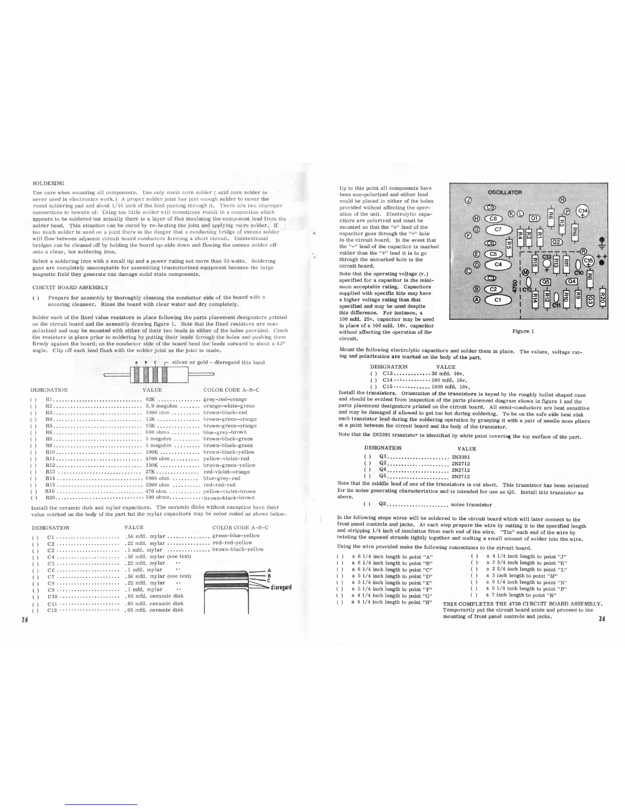
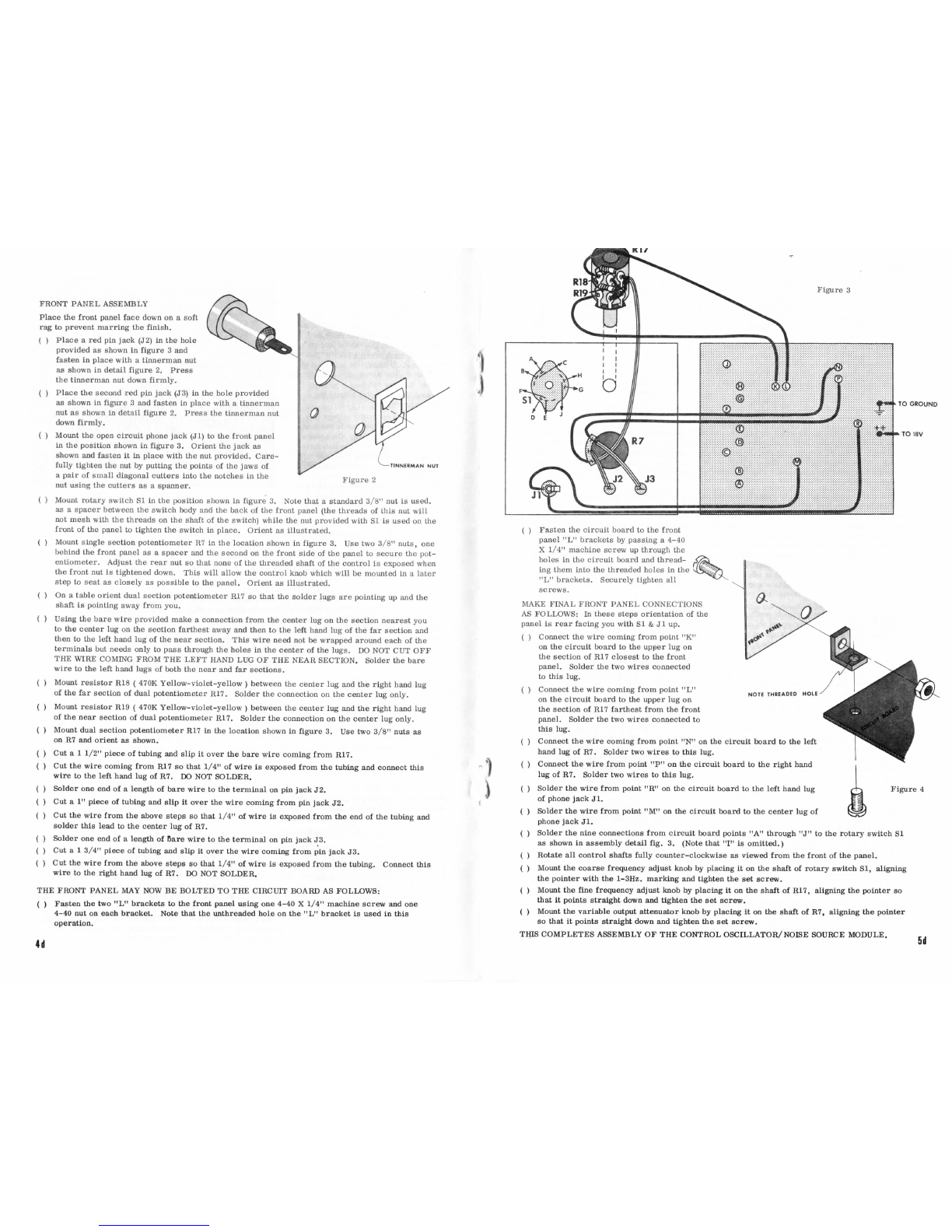
Paia 4750 User manual

?.
a„±:,ir-i; :=II
aA
5CJ'
:=:III,,:s==o:o
I-a
II
;+.cke: :8
8I
CD
IIin®®Of"
=€;ia !g
§=
®HVAau'„-I,,ii*`*® 3
Li `95§=§g
911
lLrd -
®
8=
£=
h,
®=
±:£=
§
aLio!+O , , il;, , Ei+I
!1=?1s 5fE
•
'1' I I
47=EJ
Eontrol E]sci llator/Noise =ource
The 4750 Control Oscillator / Noise source is a dual function module providing
a source of slowly varying sinusoidal control voltage for tremolo, vibrato. filter
9weeplng, eta. and a white noise source useful in a variety Of special effects
lncludlng wind and surf sounds.
SPECIFICATIONS
Module Power
Requirements ........................ 18v. @ 1. 75 rna.
OSCILLATOR
sinusoidal
Output impedance .................... Nominal 5K or less
Output Amplitude .................... One fixed 5v. p-p output
One variable 0 to 5v. p-p
Out|]ut Of D. C. blae .................. 50% Of peak to peak value
Freq`ieney range ..................... 1 to 25 Hz in three overl&pplng ranges.
NOISE SOURCE
Brondband noise
nominal loo Hz to 10 kHz.
0`rtyut Impedance .................... Nomlml lK
Output Amplitude .................... 5v. p-p
Output D. C. bla.a .................... None
© 1980 by PAIA Elect,ronlcs, hc. All Rights Reserved

SOLDERING
Use care when mounting all components. Use only rosin core solder ( acid core solder is
never used in electronics work. ) A proper solder joint has just enough solder to cover the
round soldering pad and about 1/16 inch of the lead passing through it. There are two improper
connections to beware of: Using too little solder will sometimes result in a connection which
appears to be soldered but actually there is a layer of flux insulating the component lead from the
solder bead. This situation can be cured by re-heating the joint and applying more solder. If
too much solder is used on a joint there is the danger that a conducting bridge of excess solder
will flow.between adjacent circuit board conductors forming a short circuit. Unintentional
bridges can be cleaned off by holding the board up-side down and flowing the excess solder off
onto a clean, hot soldering iron.
Select a soldering iron with a small tip and a power rating not more than 35 watts. Soldering
guns are completely unacceptable for assembling transistorized equipment because the large
magnetic field they generate can damage solid state components.
CIRCUIT BOARD ASSEMBLY
( ) Prepare for assembly by thoroughly cleaning the conductor side of the board with a
scouring cleanser. Rinse the board with clear water and dry completely.
Solder. each of the fixed value resistors in place following the parts placement designators printed
on the circuit board and the assembly drawing figure 1. Note that the fixed resistors are non-
polarized and may be mounted with either of their two leads in either of the holes provided. Cinch
the resistors in place prior to soldering by putting their leads thl`ough the holes and pushing them
firmly against the board; on the conductor side of the board bend the leads outward to about a 45°
angle. Clip off each lead flush with the solder joint as the joint is made.
A P i r Silverorgold-disregardthisband
VALUE
82K..............
3. 9 megohm .......
1000 ohm ..........
15K...............
15K...............
680 ohms ..........
1 megohm .........
1 megohm .........
|00K..............
4700 ohm ..........
150K..............
27K...............
6800 ohm .........
2200 ohm .........
470 ohm ..........,
COLOR CODE A-B-C
grey-red-orange
orange-white-green
brown-black-red
brown-green-orange
brown-green-orang.e
blue-grey-brown
brown-black-green
brown-black-green
brown-black-yellow
yellow-violet-red
brown-green-yellow
red-violet-orange
blue-grey-red
red-red-red
yellow-violet-brown
100 ohms ............ brown-black-brown
Install the ceramic disk and mylar capacitors. The ceramic disks without exception have their
value marked on the body of the part but the mylar capacitors may be color coded as shown below:
DESIGNATI0N
Zd
VALUE
.56 mfd. mylar ........
. 22 mid. mylar ........
.1 mid. mylar ,.......
. 56 mfd. mylar (see text)
.22 mfd. mylar u
.1 mfd. mylar H
. 56 mfd. mylar (see text)
.22 mfd. mylar u
.1 mfd. mylar ..
. 05 mfd. ceramic disk
. 05 mid. ceramic disk
. 05 mfd. ceramic disk
C0IjoR CODE A-B-C
green-blue-yellow
red-red-yellow
brown-black-yellow
Up to this point all components have
been non-polarized and either lead
could be placed in either of the holes
provided without affecting the oper-
ation of the unit. Electrolytic capa-
citors are polarized and must be
mounted so that the ''+" lead of the
capacitor goes through the 't+' hole
in the `circult board. In the event that
the ''-" lead of the capacitor is marked
rather than the ''+' lead it is to go
through the unmarked hole in the
circuit board.
Note that the operating voltage (v.)
specified for a capacitor is the mini-
mum acceptable rating. Capacitors
supplied with specific kits may have
a higher voltage rating than that
specified and may be used despite
this difference. For instance, a
100 mid. 25v. capacitor may be used
in place of a 100 mid. 16v. capacitor
without affecting the operation Of the
circuit.
Figure 1
Mount the following electrolytic capacitors and solder them in place. The values, voltage rat-
ing and polarization are marked on the body Of the part.
D E SIGNATI0N VA LUE
30 mid. 10v.
100 mfd. 16v.
C15 ............. 1000 mfd. 16v.
Install the translators. Orientation Of the transistors ls keyed by the roughly bullet shaped case
and should be evident from inspection of the parts placement diagl.am shown in figure 1 and the
parts placement designators printed on the circuit board. All semi-conductors are heat sensitive
and may be damaged if allowed to get too hot during soldering. To be on the safe side heat sink
each transistor lead during the soldering operation by grasping it with a pair of needle nose pliers
at a point betweeD the circuit board and the body of the transistor.
Note that the 2N3391 tl.ansistor is identified by white paint covering the top surface of the part.
DESIGNATION
VALUE
2N3391
2N2712
2N2712
2N2712
Note that the middle lead of one of the transistors is cut short. This transistor has been selected
for its noise generating characteristics and is intended for use as Q3. Install this transistor as
above.
( ) Q3 ...................... noisetransistor
In the following steps wires will be soldered to the circuit board which will later connect to the
front panel controls and jacks. At each step prepare the wire by cutting it to the specified length
and stripping 1/4 inch of insulation from each end Of the wire. ''Tin" each end of the wire by
twisting the exposed strands tightly together and melting a small amount of solder into the wire.
Using the wire provided make the following cormections to the circuit board.
a 6 1/4 inch length to point ''A"
a 6 1/4 inch length to point ''8"
a 6 I/4 inch length to point ''C"
a 5 1/4 inch length to point "D"
a 5 1/4 inch length to point ''E"
a 5 1/4 inch length to point ''F"
a 4 1/4 inch length to point ''G"
( ) a 4l/4inchlengthtopeint"J"
( ) a 23/4inchlengthtopolnt"K"
( ) a 23/4inchlengthtopoint"L"
( ) a 5inchlengthtopoint"M"
( ) a 61/4inchlengthtopoint"N"
( ) a 61/4inchlengthtopoint"P"
( ) a 7inchlengthtopoint"R"
a 41/4 inch length to point "H" TH|s conmLETES THE 4750 CIRCUIT BOARD ASSEMBLY.
Temporarily put the circuit board aside and proceed to the
mounting of front panel controls and jacks.
3d

FRONT PANEL AssEmeL¥
Place the front panel face down on a soft
rag to prevent marring the finish.
( ) Place a red pin jack (J2) in the hole
provided as shown in figure 3 and
fasten in place with a tinnerman nut
as shown in detail figure 2. Press
the tinnerman nut down firmly.
( ) Place the second red pin jack (J3) in the hole provided
as shown in figure 3 and fasten in place with a tinnerman
nut as shown in detail figure 2. Press the tinnerman nut
down firmly.
( ) Mount the open circuit phone jack (J1) to the front paLnel
in the position shown in figure 3. Orient the jack as
shown and fasten it in place with the nut provided. Care-
fully tighten the nut by putting the points of the jaws of
a pair of small diagonal cutters into the notches in the
nut using the cutters as a spanner.
( ) Mount rotary switch Sl in the position shown in figure 3. Note that a standard 3/8" nut is used.
as a spacer between the switch body and the back of the front panel (the threads of this nut will
not mesh with the threads on the shaft of the switch) while the nut provided with Sl is used on the
front of the panel to tighten the switch in place. Orient as illustrated.
( ) Mount single section potentiometer R7 in the location shown in figure 3. Use two 3/8" nuts, one
behind the front panel as a spacer and the second on the front side of the panel to secure the pot-
entiometer. Adjust the rear nut so that none of the threaded shaft of the control is exposed when
the front nut is tightened down. This will allow the control knob which win be mounted in a later
step to seat as closely as possible to the panel. Orient as illustrated.
( ) On a table orient dual section potentiometer R17 so that the solder lugs are pointing up and the
shaft is pointing away from you.
( ) Using the bare wire provided make a connection from the center lug on the section nearest you
to the center lug on the section farthest away and then to the left hand lug of the far section and
then to the left hand lug of the near section. This wire need not be wrapped around each of the
terminals but needs only to pass through the holes in the center of the lugs. DO NOT CUT OFF
THE WIRE COMING FROM THE LEFT HAND LUG OF THE NEAR SECTION. Solder the bare
wire to the left hand lugs of both the near and far sections.
( ) Mount resistor Rl8 ( 470K Yellow-violet-yellow ) between the center lug and the right hand lug
of the far section of dual potentiometer R17. Solder the connection on the center lug only.
( ) Mount resistor. Rl9 ( 470K Yellow-violet-yellow ) between the center lug and the right hand lug
of the near section of dual potentiometer R17. Solder the connection on the center lug only.
( ) Mount dual section potentiometer R17 in the location shown in figure 3. Use two 3/8" nuts as
on R7 and orient as shown.
( ) Cut a 1 I/2" piece of tubing and slip it over the bare wire coming from R17.
( ) Cut the wire coming from R17 so that 1/4" of wire is exposed from the tubing and comect this
wire to the left hand lug of R7. DO NOT SOIDER.
( ) Solder one end of a length of bare wire to the terminal on pin jack J2.
( ) Cut a 1" piece of tubing and slip it over the wire coming from pin jack J2.
( ) Cut the wire from the above steps so that I/4" of wire is exposed from the end of the tubing and
solder this lead to the center lug of R7.
( ) Solder one end of a length of bare wire to the terminal on pin jack J3.
( ) Cut a 1 3/4" piece of tubing and slip it over the wire coming from bin jack J3.
( ) Cut the wire from the above steps so that 1/4" of wire is exposed from the tubing. Connect this
wire to the right hand lug of R7. DO NOT SOLDER.
THE FRONT PANEL MAT NOw BE BOLTED TO Tlm clRculT BOARD As FOLLOws:
( ) Fasten the two ''L" brackets to the front panel using one 4-40 X 1/4" machine screw and one
4-40 nut on each bracket. Note that the unthreaded hole on the ''L" bracket is used in this
operation.
4d
( ) Fasten the circuit board to the front
panel ''L" brackets by passing a 4-40
X i/4" machine screw up through the
holes in the circuit board and thread-
ing them into the threaded holes in the
''L" brackets. Securely tighten all
screws.
MAKE FINAL FRONT PANEL CONNECTIONS
AS FOLLOWS: In these steps orientation of the
panel is rear facing you with S1 & Jl up.
( ) Connect the wire coming from point ''K"
on the circuit board to the upper lug on
the section of R17 closest to the front
panel. Solder the two wires cormected
to this lug.
( ) Connect the wire coming from point ''L"
on the circuit board to the upper lug on
the section of R17 farthest from the front
panel. Solder the two wires connected to
this lug.
( ) Connect the wire coming from point ''N" on the circuit board to the left
hand lug of R7. Solder two wires to this lug.
( ) Connect the wire from point ''P" on the circuit board to the right hand
lug of R7. Solder two wires to this lug.
( ) Solder the wire from point "R" on the circuit board to the left hand lug
of phone jack J1.
( ) Solder the wire from point ''M" on the circuit board to the center lug of
phone jack I1.
( ) Solder the nine counections from circuit board points ''A" through `'J" to the rotary switch Sl
as shown in assembly detail fig. 3. (Note that "I" is omitted. )
( ) Rotate all control shafts fully counter-clockwise as viewed from the front of the panel.
( ) Mount the coarse frequency adjust knob by placing it on the shaft of rotary switch S1, aligning
the pointer with the 1-3Hz. marking and tighten the set screw.
( ) Mount the fine frequency adjust knob by placing it on the shaft of R17, aligning the pointer so
that it points straight down and tighten the sot screw.
( ) Mount the variable output attenuator knob by placing it on the shaft Of R7, aligning the pointer
so that it points stralgbt down and tighten the set screw.
TIIIs coMPLETEs ASSEmeL¥ oF THE CONTROL osclLI.ATOR/NolsE souRCE MODul.E.
5d

TESTING
OSCILLATOR Apply an 18v. power supply (4771 power supply or other suitable supply such as
two 9v. batteries) to the H and ground cormections on the rear of the 4750 circuit board. The
control oscillator is most easily tested using an oscilloscope but a volt-ohm meter can be used.
If an oscilloscope is available connect its veltical input to the fixed 5v. p-p output of the oscil-
lator and observe that the output is approximately 5 volts peak to peak. If the oscilloscope has
a calibrated horizontal time sea.Ie check to make sure that the per.iods of oscillation agree with
the table below at the control settings indicated.
S1
1-3
1-3
3-9
3-9
9-25
9-25
R17 (Freq. ) PERIOD
(c.c.w.) Min. 1 see.
(c.w.) Max. 330 ms.
Min. 350 ms.
Max. 120 ms.
Min. 125 ms.
Max. 45 ms.
Due to component tolerances exact agreement is unlikely but observed periods should be within
20% of the above values. With this check completed connect the oscilloscope vertical input to
the variable output J2 and observe that the attenuator R7 varies the output from Ov. to 5v. peak
to peak. When observing the oscillator wave form on an oscilloscope you may note a slight flattenT
ing on the bottom Of the sine wave. This flattening is normal and will not significantly affect the
operation of the unit.
Operation of the oscillator can be roughly checked using only a volt-ohm meter as follows: Set
the VOM to a range that will produce a 1/2 to full scale deflection for 5v. (e.g. a lov. range)
and connect the meter between the ground and fixed output with the positive lead to J3. Set
frequency range switch Sl to the 1 - 3 Hz. range and rotate frequency control R17 fully counter-
clockwise. Most meters will not accurately follow a 1 Hz. signal but you should be able to see
the pointer swinging up and down and the extremes Of the swing should center about the 2. 5v. mark
on the meter (for example between 1. 5 and 3. 5). Advance the freq. control and note that the rate of
oscillation increases. As both the freq. range switch and freq. control are advanced the meter point-
er should move less and less until at some point it stops at about 2. 5v. ( allow ± 20%). Now change
the positive meter lead to variable output J2 and observe that the attenuator varies the output level
from Ov. to about 2. 5v.
Noise Source The noise source is easily cested using either an audio amplifier or oscilloscope. If
an oscilloscope is available comect the noise output jack Jl to the vertical input of the scope and ob-
serve that the peak to peak amplitude of the characteristicly fuzzy noise signal is approximately 0. 5v.
The noise effect is best observed with a sweep rate of about 2 ms. /cm. (repetition rate of about
50/second on oscilloscopes without a calibrated time base). If an amplifier is handy the output of the
noise source can be jumpered directly to the high level input of the amplifier. Test for an even
coloration of the noise by altemately advancing and retarding the bass and treble tone controls of
the amplifier. During this test the character of the noise should change noticeably (this will Of
course depend on the characteristics of the amplifier's tone control).
USING THE 4750 CONTROL OSCILLATOR/NOISE SOURCE MODUI.E
jh
The decision to make the Noise Source and Control Oscillator one module was based on many
considerations involving cost, size, versatility, etc. Neither the control oscillator nor the
noise source are items that are likely to be duplicated within any single system yet one of
each is highly desiraLble. Also, the number of knobs required by the control oscillator dictates
a double module (4" X 4") size while the electronics could easily fit on a single module circuit
board.
OPERATION OF TIE CONTROLS IS AS FOLLOWS:
:o°r£=%fFthReE%:gu¥:Ypan:1:e;°harreseeofvreerq,uaepnpc#:::::ctyher:°gn::°:]i:wthteh:Popsec:[i:::f:d
generate any frequency in the 1 to 25 Hz. range.
EEEQ. The freq. control allows the selection of any particular fl.equency within the range
selected by the Coarse Frequency control.
VARABLE OUTPUT The output jack lnarked "variable" provides an output voltflgu thilt ls
continuously variable between 0 and 5v. peak to peak, adjustable by means of .lio coi`trol
immediately to the 1-eft of the jack.
E± This output jack provides a non-adjustable source of control voltaBo thl`t ls always
5v. peak to peak at the rate set by the frequency controls.
NOISE The noise output jack provides capacitively coupled source uf . 5v. I)o{ik l{t i)Oak broad-
band noise.
The two most obvious uses for the control oscillator are producing tremolo and vibrato. Tremolo
is a rapid amplitude modulation of a musical waveform and this effect is produced by using the
oscillator output as one of the inputs to the Voltage Controlled Amplifier ( VCA ). The sinusoidal
output of the oscillator altemately increases and decreases the galn of the VOA and consequently
the amplitude of the output waveform. Vibrato is a rapid change in the pitch of a musical note
and is produced by using the oscillator as one of the inputs to the Voltage Controlled oscillator
( VCO ).
Another possible use for the Control Oscillator is as a "sweeping" signal for a Voltage Controlled
Filter ( VCF ). Once again the output of the Control Oscillator is used as one of the control in-
puts of the filter and as the oscillator output makes its cyclic change it changes the characteristics
of the filter. Typical of the effects produced in this manner would be an automatic 'Waa-Waa" if
the oscillator were driving the band-pass filter.
The Control Oscillator is not limited to driving a VCO, VCA or VCF; the output is short circuit
protected and cannot be damaged short of plugging it directly into a 110v. wall outlet. For instance,
while it is not immediately obvious. the Control Oscillator can serve as a trigger source for the
4740 envelope generator. By jumpering the variable output of the Control Oscillator into the
"trigger jaclr' on the envelope generator it is pessible to produce repeating waveforms with a
variety Of off time, rise time, fall time and sustain time charaLcteristics.
At some point on the output sinusoid of the Control Oscillator -the exact point is controllable using
the control oscillator output attenuator - the function generator will trigger and generate an output
waveform whose attack and decay times are independently variable. Repetition rate of the function
generator output is adjustable with the frequency controls of the control oscillator.
Noise is a very difficult thing to describe in other than technical terins but for our purposes we
will define it as unvoiced sound, unvoiced in that it ha,s no definite pitch or timbre like voiced sounds
such as sine or square waves do. At first thought lt might seem that there wouldn't be much you
could do with an unvoiced sound when in fact it is one of the most versatile building blocks in the
electronic musician's bag of tricks. For instance the sound Of a cymbal is synthesized using noise.
Run the noise output into a band-pass filter set to a high "Q" and a high frequency ( see 4730
Filter Instmctions) and nm the output of the filter into the audio input of a VCA which is in
turn under the control of the envelope generator set to give a rapid attack and moderate decay.
Every time the manual trigger is pressed out comes a cymbal sound.
The sound of the surf is easy to duplicate using noise. Run the output of the noise source into the
input of a Voltage controlled low pass filter and the output of the filter into the audio input of a VCA,
Control both VCF and VCA from the same output of the function generator set for long attack and
decay and when the manual trigger is pressed out comes an ocean wave. For this effect it will
also be necessary to ''bias" the VCF and VCA slightly as explained in the 4771 Power Supply instructions.
The sound of the wind can be synthesized by running noise through a VCA and band pass filter. If one of
the bias controls on the power supply is used as the control voltage source for both modules the wind can
be made to whistle by randomly tuning this control up and down. If a linear controller is used as the
control voltage source for the VCF the wind can be played like a musical instrument.
DESIGN ANALYSIS
Control Oscillator The control oscillator circuit is a common phase shift type with transistor
Ql providing gain
and 180° of phase shift while the remaining 180° of required phase shift is
provided by the pi network C1 -C9 and R4. R5 and R17 -R19. Emitter follower buffer Q2
isolates the load from the oscillator stage.
The only thing unusual about the design of the oscillator is the switching of capacitors C1-C9.
Referring to schematic diagram figure 5 you can see that in the 1-3Hz. position of S1, Cl is in
parallelwith C3. C4 with C6 and C7 with C9. In this position the total capacitance in each branch
of the pi network is . 66 mid. in the 3-9 Hz. position the series combination of Cl and C2 is in
Parallel with C3, C4 and C5 in parallel with C6, C7 and C8 in parallel with C9. This arrange-
ment gives a total capacitance of approximately . 2 mfd. In the 9 -25 Hz.position C3, C6 and C9
are the oi`1.y capacitors in the cirouit for a total capacitance in each branch of .1 mid.
Noise S{.ul.co As can be seen from the schematic diagram figure 5 the noise source is a very
simple oll` ,,,, I,.
Transistor Q3 is a silicon type that has a low emitter to base breakdown volt-
age ratln#. 'l`Iio l8v. power supply iB more than enough to cause this base-emitter junction to
operate 11` nii iLVLLLunche condition.
Resistor l`H IIi Lli(_` lmBe circuit of Q31imits the current flow through the junction and also serves
as a lon{l ri`Hliillii. rt)r the shot noise that results from the avalanche process. The random ac
voltage flu{`t,`nil,lwm I)i`ttduced by the avalanche are coupled into a single common emitter anplifier
stage ({W Ilil.nnr.,Ii (HL|jiicltor Cl1. This first stage not only boosts the signal silghtly but also ser-
ves a8 i`l` linii``iliii`{``t iiiutching element between the noise source and the main amplifier Q5. The
ampllfLt`Il iil.LH(I lH (`I>iip'led by C12 to the front panel output jack.
iA
Other Paia Recording Equipment manuals