Paia 4780 User manual

ELECTRONICS, INC.
=EOUENCER
ASSEMBLY
INSTRuCTloNS
47=EJ
In basic terms, a sequencer is simply another control voltage and trigger source. UDlike
other controllers, howevel.; it allows the user to pre-program an extended sequence of
control voltage variations that can be called up on command and allows the variations to
be executed at speeds beyond human capabilities. In addition to their obvious applications
in generating fast arpeggios and automatic bass lines, sequencers can also be used as
programmable function generators, counters or clock sources.
Considerable time and effort has gone into making the PAIA 4780 as versatile as possible
without losing the user in a hopeless tangle of operational details. Many of the internal
"housekeeping" functions are automatic yet externally available inputs and controls permit
by-passing automatic functions in favor of manual control.
© 1975 PAIA Electronics, Inc.1020 W. Wilshire Blvd. , Oklahoma City, OK 73116

SPECIFICATIONS
Power requlrenientB: + 18 v. @ 50 rna.
± 9v. @ 1 rna.
Clock rate: 2/see. to 32/see.
Control voltage range: 0 -5 v. nominal
Addltlonal features: Built in glide
Light Emitting Dlode lndlcates clock rate
LED Stage Status indicators
Manual and eleetrlcly activated controls
2 to 12 event re-circulating count capabilities.

SOIjDEluNG
Use care when mounting all components. Use only rosin core solder (acid core solder is never used
in electronics work. ) A proper solder joint has just enough solder to cover the I.ound soldering pad
and about 1/16 inch of the lead passing through it. There are two improper comections to beware of:
Using too little solder will sometimes result in a connection which appears to be soldered but actually
there is a layer of flux insulating the component lead from the solder bead. This situation can be
cured by re-heating the joint and applying more solder. If too much solder is used there is the danger
that a conducting bridge of excess solder will flow between adjacent circuit board conductors forming
a short circuit. Unintentional solder bridges can be cleaned off by holding the board up-side down and
flowing the excess solder off onto a clean hot soldering iron.
Select a soldering iron with a small tip and a power rating not more than 35 watts. Soldering guns are
completely unacceptable for assembling transistorized equipment because the large magnetic field they
generate can damage solid state components.
CIRCUIT BOARD ASSEMBLY
( ) Prepare for assembly by thoroughly cleaning the conductor side of the smaller "A" ciroult
board with a scouring cleanser. Rinse the board with clear water and dry completely.
Solder each of the fixed resistors in place following the parts placement designators printed on the
circuit board and the assembly drawing figure 1. Note that the fixed value resistors are Don-polarized
and may be mounted with either of their two leads in either Of the holes provided. Cinch the resistors
in place prior to soldering by putting their leads through the holes and pushing them fil.mly against the
board; on the conductor side of the board bend the leads outward to about a 45° angle. Clip off each
lead flush with the solder joint as the joint is made. Save the lead clippings for use as jumpers in
later steps.
A P i silverorgold-disregardthisband
DESIGNATION
COLOR CODE A-B-C
brown-green-yellow
brown-green-yellow
brown-green-yellow
brown-green-yellow
brown-green-yellow
brown-green-yellow
brown-black-red
brown-black-red
brown-black-red
brown-black-red
brown-black-red
brown-black-red
blue-grey-yellow
orange-orange-yellow
red-red-yellow
orange-white-green
brown-black-green
red-red-green
brown-black-green
yellow-violet-I`ed
brown-green-orange
orange-orange-orange
brown-green-yellow
blue-grey-brown
brown-black-green
brown-black-orange
brown-black-brown
orange-orange-yellow
brown-green-orange
brown-black-red
brctwn-green-yellow
red-red-orange
yellow-violet-yellow
brown-black-green
orange-orange-orange
DESIGNATI0N
#ar: I;
VALUE
47K ..
1meg
1 meg ,
COLOR CODE A-B-C
yellow-violet-orange
brown-black-green
brown-black-green
6. 8K ................... blue-grey-red
10K...................brown-black-orange
Install the ceramic disk capacitors. Without exception the value will be marked on the body Of the
part.
DE sroNATio N vA LUE
E=
. 001 mfd. oeramlc disk.
100 pf. ceramic diskik
. 05 mfd. ceramic disk
. 05 mid. ceranic disk
Up to this point all components have been ron-polarized and either lead could be placed in either of
the holes provided without affecting the operation of the circuit. Electrolytic capacitors are polarized
and most be mounted so that the ''+ " lead of the capacitor goes through the ''+ " hole in the circuit
board. In the event that the ''-'' lead of the capacitor is marked rather than the " + " lead it is to go
throngh the unmarked hole in the circuit board.
Note that the operating voltage (v. ) specified for a capacitor is the minimum acceptable rating.
Capacitors supplied with specffic kits may have a higher voltage rating than that specified and may
be used despite this difference. For instance. a 100 mid. 25v. capacitor may be used in place of
a 100 mid. 10v. capacitor without affecting the operation Of the circuit.
Mount the following electrolytic capacitors and solder them in place. The values, voltage rating and
polarization are marked on the body Of the part.
uH,?AI"::
u.
C5
VALUE
2. 2 mid. 10v. electrolytic
2. 2 mfd. 10v. electrolytic
hstall the transistors. Orientation Of the transistors is keyed by the flat on the side of the case and
should be evident from inspection of the parts placement diagram shown in figure 1 and the parts
placement designators printed on the circuit board. All semi-conductors are heat sensitive and may
be damaged if allowed to get too hot during soldering. To be on the safe side heat sink each transistor
lead during the soldering operation by grasping it with a pair of needle-nosed pliers at a point between
the circuit board and the body of the transistor. The part type no. is printed on the case.
DESIGNATION TYPE NO.
#,y i:
2N5129
2N5129
2N5129
Install the diodes. Note that these parts are polarized and must be
properly oriented in order to
operate correctly. Polarization of the diodes is indicated by a colored band on one end of the case.
Install as shown in figure 1. The physical appearance Of the device is related to the schematic
symbol used on the circuit board parts placement designators in the drawing below.
DESIGNATION
(¥z :i
TYPE NO.
|N914
|N914
Using the excess resistor leads clipped from resistor installation. form and install the
wire jumper indicated by the solid line printed on the circuit board and shown in the parts
placenien( diagrar.I figure 1,
Install the trin`mJ=r potf,ntiometer.
:?i.- .`
NATION
R37
VALUE
50K trimmer potentiometer

IE
Prepare for assembly by thoroughly cleaning the conductor side of the ''8" circuit
hstall the multi-turn potentiometers R41 through R46. Install the controls by pushing all three
pins through the holes provided in the clrcutt board and then soldering only the pin closest to the
edge of the circuit board. Make sure that the control is perpendicular before soldering the rear
two pins of each control.
(#ty- E::
(i£ , R43
(ay,' R44
(`Y R45
(i R46
50K multi-turn
50K multi-turn
50K multi-turn
50K multi-turn
50K multi-turn
50K multi-turn
When these controls have been Soldered in place, carefully pull the knobs from the shafts. Save
the lmobs for re-lngtallatlon in later steps.
Mount the integrated circuit. Note that the orientation of the integrated circuit is keyed by a notoh
at one end of the case which aligns with the semi-circular key on the de8ignator printed on the circuit
board. Use particular care when installing this part, like any other semi-conductor it iB heat sensi-
tive and should not be exposed to extraordinarily high soldering temperatures. Make Sure that the
orientation is correct before soldering. once the unit is in place it cannot be removed without destroying
destroying it.
DESIGNATION TYPE NO.
ut
IC-1 ...................... LM3900 or
CA3401E Quad Norton Amplifier
h the following steps wires will be soldered to the clrcult board which will later connect to tbe
front panel controls and jaekB. At each step prepare the wire by cutting it to the Specified length
and stripping 1/4 inch of insulation from each end Of the wire. ''Tin" each end of the wire by
twisting the exposed strands tightly together and melting a small amount of solder into the wire.
Using the wire provided make the following connections to the ''A" circuit board.
A 10 inch length to point 'W''.
4-1/2 inch length to point ''H''.
5 inch length to point ''J''.
4-3/4 inch length to point ''K".
4-1/2 inch length to point ''L''.
6-1/2 inch length to point ''M''.
4 inch length to point ''N''.
6 inch length to point ''P''.
6-1/2 inch length to poitit ''R''.
6-3/4 inch length to point ''S''.
1-1/4 inch length to oof nt 'T''.
6 inch length to point ''AJ3''.
1-I/2 inch length to point ''A''.
1-1/2 inch length to point "8''.
1-1/2 inch length to point "C''.
1-1/2 inch length to point ''D"
1-1/2 ilich length to point ''E'1.
1-1/2 inch length to point ''F".
1-3/4 inch length to point ''G''.
Pass the wires from points A, 8, C, D, E and F through the unmarked holes adjacent to each point.
Tj-:
/
(+,.,
4
11 facilitate their connection to front panel jacks in later Steps. See ligure 2.
Prepare the 2-1/4 inch piece of RG-154/U co-axial cable provided by 8trlpping 1/2 inch
Of the black outer insulatioD from each end. Carefully un-brald the shielding to apose
the insulated inner conductor. Twist the loosened braid back together and lightly "tin"
the end. Remove 1/4 inch Of insulation from the irmer conductor at each end (Bee figure 3)
At one end of the cable prepared above connect the tinned shield to circuit board point
'rv.l and solder.
Comect the inner conductor Of the cable prepared above to circuit board point 'U''.
TELS CoMPLETEs AssErmL¥ oF THE ..A.i clRculT BOARD. TEMpoRAluL¥ SET THE CIRCulT
BOARD AslDE AND pROcEED VITH THE AssErmLy OF THE 4780 I.Bw clRcurr BOARD.
board with a scouring cleanser. Rinse with clear water and dry completely.
Following the directions given for resistor installation on the ''A" circuit board, install the fixed
value resistor.s on the ''8" circuit board as follows. Save the resistor lead clippings for use in
later steps. See figure 4.
DESIGNATION
( i,, R48
( ty,,`
lEi=
DE=|
(#
:i
er.
R49
R50
R51
R52
R53
R54
R55
R56
R57
R58
R59
R60
R61
R62
R63
R64
R65
R66
R67
R68
R69
R70
R71
R72
R73
R74
R75
R76
R77
R78
R79
R80
R81
R82
R83
R84
R85
R86
R87
R88
R89
R90
R91
R92
R93
R94
R95
R96
R97
R98
R99
R100
R101
R102
R103
R104
COLOR CODE A-B-C
brown-green-yellow
brown-green-yellow
brown-green-yellow
brown-green-yellow
brown-green-yellow
brown-green-yellow
brown-black-red
brown-black-red
brown-black-red
brown-black-red
brown-black-red
brown-black-red
blue-grey-brown
brown-black-orange
orange-orange-yellow
red-red-yellow
red-red-yellow
red-red-yellow
red-red-yellow
red-red-yellow
red-red-yellow
red-red-yellow
red-red-yellow
red-red-yellow
red-red-yellow
red-red-yellow
red-red-yellow
red-violet-yellow
red-violet-yellow
red-violet-yellow
red-violet-yellow
red-violet-yellow
red-violet-yellow
red-violet-yellow
red-violet-yellow
red-violet-yellow
red-violet-yellow
red-violet-yellow
recl-violet-yellow
orange-orange-yellow
red-red-yellow
red-red-yellow
red-red-yellow
red-red-yellow
red-red-yellow
red-red-yellow

DESIGNATI0N
!%
(+`
IEE,
:.f`
(i.`
ff3FL
R105
R106
R107
R108
RIO9
R110
R11|
R112
R113
R114
R115
R116
R117
R118
R119
R120
R121
R122
R123
(V' R130
(¥;
:i.
(iF
:i`
(d¢,fry
R131
R132
R133
R134
R140
R141
R142
R143
100K...............
LOOK................
2. 2 meg ohm .,......
330K
IK..................
1K..................
47 ohms ..............
330K.....'..........
|00K................
33K.................
680 ............. ' . . .
10K.................
COLOR CODE A-B-C
red-red-yellow
red-red-yellow
red-red-yellow
red-red-yellow
red-red-yellow
red-red-yellow
brown-black-yellow
brown-black-yellow
brown-black-yellow
brown-black-yellow
brown-balck-yellow
brown-black-yellow
brown-black-yellow
brown-black-yellow
brown-black-yellow
brown-black-yellow
brown-black-yellow
red-red-green
orange-orange-yellow
brown-black-red
brown-black-red
yellow-violet-black
orange-orange-yellow
brown-black-yellow
orange-orange-orange
blue-grey-brown
brown-black-orange
Install the ceramic disk capacitors. The values Of these capacitors are marked on the body of the
part.
:::.
HEE
(y,
01 mid. ceramic disk
005 mid. ceramic disk
01 mid. ceramic disk
01 mfd. ceramic disk
01 mid. ceramic disk
. 01 mfid.
. 01 mfd.
. 01 mid.
• 01 mfd.
• 01 mfd.
• 01 mfd.
• 01 mfd.
ceramic disk
ceramic disk
ceramic disk
ceramic disk
cerahic disk
ceramic disk
ceramic disk
loo p£. ceramic disk
. 005 mid. ceramic disk
Following the directions given for capacitor installation on the ''A" circuit board, install the
electrolytic capacitors on the ''8" circuit board as follows:
DE SIG NATION DE SC RIPI`ION
(rtysatf,
(i`
(dy--`:
HfiL
2. 2 mid. 10v. electrolytic
1000 mid. 25v. electrolytic
33 mid. 16v. electrolytic
Following the instructions given for diode installation on the ''A" circuit board, install the diode8 on
the ''8" circuit board as follows:
D3......................1N914
D4 ...................... 5. 6v. Zener
6
(jry'`' U8ing the excess resistor leads Clipped from resistor installation, form and install the 7
wire jumpers indicated by the solid lines printed on the clrouit board and shown in the parts
olacement diagram figure 4.
Install the multi-ton potentlometers R124 through R129. Install the controls try pushing an
three pins through the holes provided in the circuit board and then Soldering only the pin Closest
to the edge of the olrcuit board. Make sure that the control is perpendicular before soldering
the rear two pins Of each control.
ar' Ri24
(ryy` Ri25
( YF R126
(t - R127
( T,_ R128
(i- R12 9
50K multi-turn
50K multi-turn
50K multi-turn
50K multi-turn
50K multi-turn
50K multi-turn
When these controls have been Soldered in place, carefully pull the knobs from the shafts.
Save the knobs for re-installation in later steps.
Following the directions given for transistor installation on the ''A" circuit board install the
transistor on the ''8" circuit board.
¥9GNA#°T....................2N3391
TYPE NO.
EE-==-fi
Mount the integrated circuits following the directions for integrated circuit installation given for
the ''A" circuit board. Make sure that orientation is correct before soldering, once the unit is
in place it cannot be removed witbout destroying lt.
IJESIGNATION TYPE NO.
LM3900 or CA34olE Quad Norton Amplifier
748 op-amp
( tylp'Y Four "fleaw clips have been included to facilitate power supply cormeetion. hsert these
clips in the holes at the end Of the circuit board marked "++". "+ ", ''-" and " i ''.
Solder in phee.
In the following steps wires will be soldered to the ''8" circuit board which will later comect with
front panel controls and jacks. At each step strip 1/4 inch of insulation from each end and twist
and ''tin" the exposed BtrandB.
UBing the wire provided make the following connections to the circuit board.
(# i :=ingief:i#iog:#ff::,',J=,"
(ijpe*£:_i3n/°4h£]necnbgr]:££°t?tp:#'i'..MMw.
A 1-1/2 inch length to point ''NN".
A 1-1/2 inch length to point ''PP''.
A 1-1/2 inch length to point ''RR''.
A 1-1/2 inch length to print "SS''.
A 1-1/2 inch length to point 'TT''.
A 1-1/2 inch length to point lruu'l.
Pass the short wires installed in circuit board points ''NN" through ''UU" through the
unmarked holes in the circuit board as shown in figure 2.
(i7giv:,:i A 1-1/2 inch lezigth to point "W".
A 1-1/2 inch length to point 'W''.
Pass the wire just installed through the unmarked hole just to the right of circuit
board point 'WW".
A 1 inch length to point ''RT'.
A 1 inch length to point 'ryY"
Pass the wire just installed in circuit board point "YY" and the wire previously in-
stalled at point "W" through the unmarked 1/8 inch hole in the circuit board just to
the right of point ''YY''.

/
A 9-1/2 inch length to point ''ZZ''.
{.rp' A 1-1/2 inch length to point "AE".
( ,3f- Pass the wire just installed through the unmarked hole directly above circuit board
(#
point ''AE„.
A 3 inch length to point ''AF''.
A 2-I/2 inch length to point "AG''.
A I-1/2 inch length to point ''AU''.
(¥ : :::,:i::: i:£: :: 3::: ,':A;:'..
(`)#'f Prepare a 2-3/4 inch length of the co-axial cable provided by stripping 1/2 inch of
insulation from one end and un-braiding the exposed shield wires. Twist the shield
wires tightly together and tin by melting a small amount of solder into the wires.
Remove 1/4 inch of insulation from the end of the exposed center conductor. Counect
the shield to cicouit board point "AK" and the inner conductor to point "AJ".
(+/Strip1/2inchoftheouterinsulationfromthefreeendofthepreviouslyinstalled
cable. Cut the braided shield flush with the outer insulation before stripping 1/4
inch Of insulation from the exposed inner conductor. Cormect the inner conductor
to circuit board point ''AL''.
Make the following interconnections between points on the ''8" circuit board.
:€.
(¥
Comect the wire from point ''GG" to point ''AT''.
Connect the wire from point ''HH" to point "AS".
Connect the wire from point ''JJ" to point ''AP''.
Connect the wire from point "KK" to point ''AR''.
Connect the wire from point ''LL" to point ''AN''.
Connect the wire from point ''MM" to point ''AM".
''Dress" the wires installed above so that they all lie flat against the circuit board. The wires
may be held in place by pressing them down between conveniently placed resistors on the
circuit board.
This completes assembly of the 4780 ''8" circuit board. Temporarily set this circuit board aside
You are now ready to put together the light emitting diode. assemblies using the small 4780/C
circuit boards. This will be a delicate assembly and the instructions should be followed
EXACTLY to assure success.
I+.
Thoroughly scour the conductor side Of the ''C" circuit boards until they are bright
and shiny. Perform this step only when ready to prcoeed with the assembly to
prevent oxidation on the circuit boards. Oxidized circuit boards will require
soldering temperatures that are higher than can be tolerated by the parts that are
to be mounted. Rinse the boards with clear water and dry completely.
(tygiv^ Cut twelve 3/4 inch lengths of the bare wire provided. Lay the boards face dowfl on the
work surface with the conductor sides up. Insert one of the twelve 3/4 inch length of bare
wire into the hole in each of the twelve soldering pads and solder in place following detail
drawing figure 5.
The boards should now have the wires protruding out the conductor side with none of the wire
protruding from the component side of the circuit board. If there is a small bit of wire crowing
on the component side, clip it off flush with the circuit board.
You are now ready to mount the Light Emitting Diodes (LEDs). Fir.st examine this part carefully
and note that one of the leads is marked with a green band. This marks the cathode of the LED.
Observe that the rear side of the case is flat, while the front side is roughly dome shaped. In a
later step the dome shaped front of the package will mate with a hole in the front panel.
Bend the leads of the LED loosely back. DO NOT use pliers to form a right angle bend in
the leads. Make sure that the green band g.oes through the hole that is pal.t of the common
strip marked ''com" on the conductor side of the board. Insert the LEDs on the component
side of the circuit board and fold the leads tightly against the solder pads. DO NOT SOLDER
YET.
It is imperative that the LEDs not be subjected to excessive soldering temperatures. Before
each LED is soldered in place, carefully scrape the j2±g!E of its lead with a razor blade or
sharp knife to remove any oxidation that may have formed. (NOTE: the green cathode band
is on the Eg±Lof the lead. )
As each lead is scraped clean lightly solder it to the circuit board pads. Clip off each lead
as short as possible after it is soldered.
( ty,-
:`i,
LED-I.
LED-2
LED-3
LED-4
LED-5
LED-6
LED-7
LED-8
LED-9
I.ED-10
LED-11
LED-12
(-fy Prepare a 2-1/2 inch length of insulated wire by removing 1/4 inch of insulation from each
end and tinning the exposed wire.
fi
Install the wire prepared above in the pad marked ''com" from the conductor side of
the ''C" circuit boards. Solder. Cut away any wire that protrudes from the component
side of the circuit board. This circuit board will become the top LED board and should
now look like the board shown in figure 6.
STOP
When this module is fully assembled the Light Emitting Diode Boards will be difficult to
service. At this point test the 4780/C boards using any size 1. 5 volt flashlight battery
as shown below. Make sure that the negative (-) terminal of the battery connects to the
''com" pad of the 4780/C board. Check polarity and soldering connections of any LED
that does not light.
Touch ''+ " of battery to each LED lead in turn.
You are now ready to connect the smaller ''C" circuit boards to the ''A" and ''8" boards. Note that
the larger boards have holes under the multi-turn potentiometers marked 1 through 6. The LED
boards have their pads numbered 1 through 6 also.
(`}~ Using the LED board with the wire installed in the "COM" pad, insert the bare wires
coming from points labeled 1 through 6 into the holes labeled 1 through 6 on the ''A"
circuit board. NOTE: These wires are to be inserted from the component side of the
''A''Circuit board. In a subsequent step this LED board will bend around so that it is in
front of the ''A" board. This will require that there be approximately 1/2 inch of the
bare wire between the two boards. The spacing will be correct if the ''C" board is just
slightly above the top of the multi-turn trimmers as shown in figure 7 when the leads
are soldered in place.
(7r'-' In a similar manner mount the remaining LED circuit board to the "B" circuit board.
(jgiv' Fasten the two "L" brackets to the "A" circuit board using one 4-40 X 1/2 inch
machine screw, one 1/4 inch spacer, one lockwasher and one 4-40 nut on each bracket as
shown in figure 8. Note that the unthreaded hole in the "L" bracket is used in this step.
\r,..,
In a similar manner fasten two ''L" brackets to the ''8" circuit board.
(tIr Position the mounting holes on the LED boards so that they are in line with the
threaded holes in-the ''L" bracket. In a later step. screws will pass through the front panel
and through the LED board into the threaded holes in the ''L" brackets.

:-;,
JP4`
(^,
(+``
In a similar manner mount black pin jack J3.
In a similar manner mount red pin jack J4.
In a similar manner mount red pin jack J5.
In a similar manner mount red pin jack J6.
In a similar manner mount red pin jack J7.
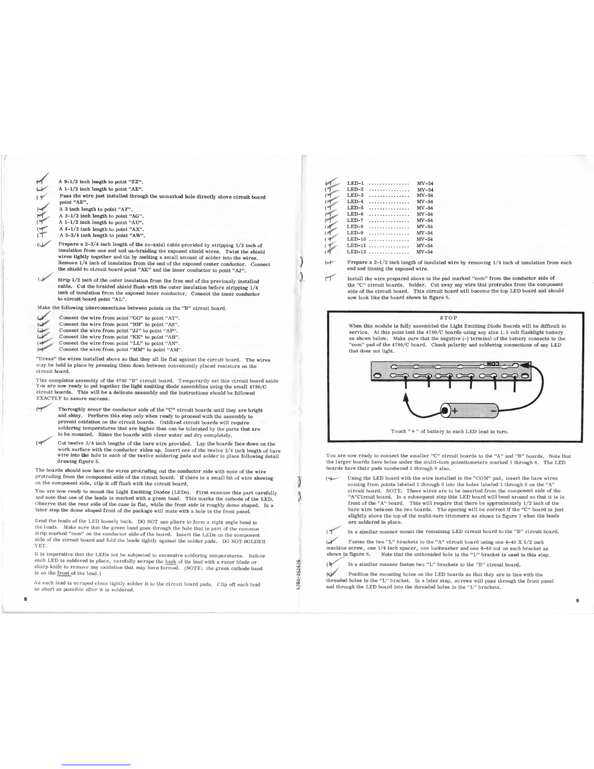
One Light Emitting Diode remains to be mounted on the ''8" board. Just to the right of
the circuit board point "WW" are two holes marked ''LED" (left side of board). Solder
two of the ''flea clips" provided into these holes. Note that when properly installed the
upright portions of the "U" shape of this clip will be pointed toward the closest edge Of
the circuit board. (see figure 9)
(q# Install the two LED supporting flea clips.
Bend the leads of the LED ±gg±±!y back and slip them into the clips such that they are roughly
parallel with the surface Of the circuit board. The ends Of the LED should be even with the rear
edges Of the clips. Make sure that the unmarked lead goes into the clip that Connects to R6o.
Lightly solder the LED leads to the clips.
Placethefrontpanelface\downonasoftragtopreventmarringthefinish.
ae`' Place a blackpin jack (J1) in thehole provided as shown in figure 10. Fasten in
place with a tinnerman nut as shown in figure 11. Press the tinnerman out down firmly.
NOTE that all tinnerman nuts must be mounted verticly as shown in figure 10.
faS Ina Similar manner mount black pinjack (J2) as shownin figure lo.
'£' -_ -.=_&`__ ___
(`y¢ In a similarmanner mount red pin jackJ8.
In a similar manner mount red pin jack J9.
In a similar manner mount red pin jack J10.
(-`) In a similar manner mou[it red pin jack Jll.
(/t In a Similar manner mount red pin jack J12.
(|`' In a similar manner mount red pin jackJ13.
(|`'' In a similarmanner mount red pin jackJ14.
(rf h a Similar manner mount red pin jack J15.
(-i ln a similar manner mount red pin jack J16.
:f//,
In a similar manner mount red pin jack J17.
In a similar manner mount red pin jack J18.
¢}p/ Using two 440 X 1/4 inch screws. two 4-40 nuts and two lock nuts, mount slide switeh s1
„.,
in the position shown ln figure 10. Make sure that the points Of the 4-40 nuts do not interfere
with the travel of the slide inside the Switch.
Mount the SPST push button switoh S2 in the position shown in figure 10. Use the lockwasher
between the rear surface Of the front panel and the body of the switoh.
In a similar manner mount pushbutton switch S3.
Mount 500K potentiometer R135 in the location shown in figure 10. Use two 3/8 inch nuts,
one behind the front panel as a spacer and the second on the front side Of the panel to secure
the potentiometer. Adjust the rear nut so that none Of the threaded shaft Of the control is
exposed when the front nut is tightened down. This will allow the control knob which will be
mounted in a later step to seat as closely as possible to the front panel. Orieut as illustrated.
(a;# In a similar manner mount 500K potentlometer R136 in the location shown in figure 10.
rfu<.L# orient as illustrated,
In a similar manner mount 75K potentiometer R137. Orient as illustrated.
In the following steps interconnection wiring will be done on the front panel controls. At each step
cut the wire to the specified length and strip 1/4 inch of insulation from each end. Twist the exposed
strands and tin by melting a small amount of solder into the wire. (Bee figure 12)
110
(.i..
HE]
Prepare a 1-1/2 inch length Of insulated wire and connect lug #2 o£ Sl and lug #3 of R135.
Solder the connection at Sl but do not solder the connection at R135 at this time.
Cut one lead of loon resistor R139 (brown-black-yellow) to a length of 1/2 inch and the
other lead to a length o£ 1 inch.
(rty D"" Pass the 1 inch lead of the previously prepared resistor through lug #3 of R137 to lug #2 Of
R137. Pass the 1/2 inch lend of this resistor through lug #1 of R137. Solder the connection
at lug #2 of R137 but do not solder the connections at lug #1 and lug #3 at this time.
(ri}. Cut both leads of 4. 7K resistor R138 tyellow-violet-red) to a length of 3/8 inch.
( +)Y Connect one lead of the previously prepared resistor to lug #1 of R136 and the other lead
to lug #3 of R136. Do not solder either connection.
S:¢bys'"' Prepare a 2 inch lengthofinsulatedwire and connect lug#1 ofs2 to lug#2 ofs3. Solder
the connection at S3 but do not solder the connection at S2 at this t`ime.
(+'~ :arcehp:::d: ]g:£]p4t::°:eeags5 obfyt::Sds££ondgeaof¥:/{4nc:c]henbgetyho:: tthhee pe`nadst;: tthuebttnugb£Pnrg:V[ded over
(dy~-' Connect the lead coming from the end of D5 that is marked with a colored band to lug #1
of S3. NOTE: Correct orientation of this diode is necessary for operation of the unit.
Solder this connection.
Connect the remaining lead of D5 to J1. DO NOT Sol.DER.
Peel the cardboard backing from the black ''dots" provided. Mount the dots over the LED
holes on the back of the front panel as shown in detail figure 10.
THE CIRCUIT BOARDS MAY NOW BE BOLTED TO THE FRONT PANEL AS FOLLOWS:
/
Using two each 4-40 X 1/4 inch screws and 61ockwashers, mount the smaller ''A"
circuit board to the front panel as shown in figure 8. Note that the ''A" circuit board will
be the top board of the two board stack and mounts approximately on an imaginary line
between R135 and R136. When mounting the board make sure that the shafts of the multi-
turn trimmers R41 through R46 align with the top-most row of large holes in the front panel.
Also make sure that the Light Emitting Diodes align with the row of smaller holes.
MAKE THE FOLLOWING CONNECTIONS BETWEEN THE ''A" CIRCUIT BOARD.AND THE
FRONT PANEL CONTROLS USING THE WIRES PREVIOUSLY INSTALLED ON THE CIRCUIT
BOARD. (see figure 13) Dress the wires against the front panel wherever possible.
rl-
Point ''J" to pin jack J1 (solder 2 wires at this point).
Point ''K" to lug #2 of R136 (solder).
Point "M" to lug #3 of S1 (solder).
Point ''P" to pin jack J16 (DO NOT SOLDER) .
Point ''R" to lug #2 of S2 (solder).
Point ''S" to lug #2 of R135 (solder).
Point ''T" to lug #3 of R136 (solder two wires).
Point ''W" to pin jack J2 (solder).
Point ''G" to lug #3 of R135 (solder two wires).
The remaining wires coming from the component side of the "A" circuit board will connect
to thg, ''8" circuit board in the following steps.
Connect the six wires that pass through the circuit board from points ''A" through
''F" to pin jacks J4 through J9 respectively. ro NOT SOLDER any of these
connections at this time.
BEFORE MOUNTING THE ''8'' CIRCUIT BOARD THERE ARE SEVEN CONNECTIONS WIIICH
MUST BE MADE TO PIN JACKS J4 THROUGH J9. h later steps these wires will connect to
points on the ''8" circuit board. Prepare each wire prior to installation by stripping 1/4 inch
Of insulation from each end and twisting and tinning the exposed strands.
A 5-1/2 inch length to J4 (DO NOT SOLDEI9
An 8 inch length to J4 (Solder three wires).
An 8 inch length to J5 (Solder two wires).
A 6-1/2 inch length to J6 (Solder two wires).
A 5 inch length to J7 (Solder two wires).
A 4 inch length to J8 (Solder two wires).
A 4-1/2 inch length to J9 (Solder two wires).

4,
fasten the ''8" board in place using two each 440 X 1/4 inch machine screws and 6 1cotwashers.
Note that diode D5 as well as the wires to S3 and J2 will be between the front panel and the
front edge of the "a" circuit board. Make sure that all seven of the LED's associated with this
circuit board align with the front panel holes provided for them.
Following the same procedure that was used while mounting the "A" circuit board,
Using the wires previously connected to pin jacks J4 throngh J9 make the following connections
to the ''8" circuit board. Solder each connection as it is made. (see figure 14)
(V# The shorter of the two leads from J4 to 'B" circuitboardpoint "AH".
The longer of the two leads from J4 to point ''88''.
The lead from J5 to point ''AA''.
The lead from J6 to point ''CC''.
The lead from J7 to point "DD''.
The lead from J8 to point ''FF''.
(J# The lead from J9 to point "EE".
MAKE THE FOLLOWING CONNECTIONS BETWEEN THE ''A" and ''8'' CIRCUIT BOARlrs.
Solder each connection as it is made. (see figul.e 15)
(7 ::i::::X:"..::::
(+f point "u" (center
conductor Of co-ax)
Point ''V" (shield of
cO-ax)...........
to ''8'' board
point ''X''.
point 'rY„
point ''Z„
point ''AB„
point ',U„
point ,rv„
Connect the short piece of insulated wire previously soldered to the ''com" terminal
of the upper LED board (4780/C) to point ''AD" of the ''B" circuit board.
IVIAKE THE FOLLOWING CONNECTIONS TO THE FRONT PANEL CONTROLS USING THE
WIRES PREVIOUSLY INSTALLED ON THE 4780/8 CIRCUIT BOARD. (See figure 14)
(ty' from point "AG" to lug #1 of pushbutton s2 (solder two wires).
(ip`, from point "AU" to pin jack J18 (solder).
EREJ
from point ''AF" to lug #1 of R136 (solder two wires).
from point "X" to pin jack J16 (solder two wires).
from point ''AX" to lug #1 of R137 (solder two wires).
from point ''AW" to lug #3 of R137 (solder two wires).
Feed the wire originating at ''8" circuit board point ''ZZ" between the front panel
and the wires connecting to pin jacks J4 through J9 and connect to lug #1 of S1 (solder).
FLIP THE MODULE OVER AND MAKE THE FOLLOWING CONNECTIONS USING THE
WIRES PREVIOUSLY PASSED THROUGH THE CIRCUIT BOARD. (see figure 16)
(`}py` Connect the wire originating at circuit board point "WW" to pin jack J17 (solder).
(t-` Connect the wire originating at circuit board point "AE" to the "com" pad of the
4780/C board. NOTE: Do not pass this wire through the hole in the "com" pad as this
presents the danger of a short circuit to the front panel. Simply lay the wire against the
pad and solder in place.
Connect the wire from circuit board point ''UU" to J15 (solder).
Connect the wire from circuit board point 'TT" to J14 (solder).
(`#`a Connect the wire from circuit board poiut "SS" to J13 (solder).
(`f Cormect the wire from circuit board point "RR" to J12 (solder)
Connect the wire from circuit board point ''PP" to Jll (solder)
Connect the wire from circuit board'point ''NN" to J10 (solder)
N# Connect tbe wire from circuit board point "VV" to J3 (solder). NOTE: Exercise
caution at this connection that the two wires coming through the single hole in the circuit
-
board are not confused.
Connect the wire coming from circuit board poiflt ''YY" to lug #1 of S3 (solder 2 wires).
THIS COMPLETES ELECTRICAL ASSEhill3LY OF THE 4780 SEQUENCER. Turn the module over
and install the 12 pitch control knobs on the shafts of the multi-turn trimmers accessible through
the holes in the front panel. Rotate the three potentiometer shafts (R135, R136 and R137) fully
counter-clockwise before pressing on the three control knobs provided. Make sure that the
pointer of each knob points to the ''7 0'clock" position of an imaginary clock face before pressing
it in place.
13
Table of contents
Other Paia Recording Equipment manuals