Panasonic KX-TEA308CE User manual

© 2005 Panasonic Communications Co., Ltd. All
rights reserved. Unauthorized copying and
distribution is a violation of law.
KX-TEA308CE
KX-TE82460X
KX-TE82492X
KX-TE82493X
KX-A227X
(for Europe)
Advanced Hybrid System
IMPORTANT INFORMATION ABOUT LEAD FREE, (PbF), SOLDERING
If lead free solder was used in the manufacture of this product the printed circuit boards will be marked PbF.
Standard leaded, (Pb), solder can be used as usual on boards without the PbF mark.
When this mark does appear, please read and follow the special instructions described in this manual on the use of PbF and how
it might be permissible to use Pb solder during service and repair work.
ORDER NO. KMS0506086CE

1 ABOUT LEAD FREE SOLDER (PbF: Pb free) 4
1.1. SUGGESTED PbF SOLDER 4
1.2. HOW TO RECOGNIZE THAT Pb FREE SOLDER IS
USED 5
2 FOR SERVICE TECHNICIANS 7
3 CAUTION 8
3.1. SAFETY PRECAUTIONS 8
3.2. INSULATION RESISTANCE TEST 8
3.3. BATTERY CAUTION 8
3.4. CAUTION 8
4 SPECIFICATIONS 9
4.1. GENERAL DESCRIPTION 9
4.2. CHARACTERISTICS 9
4.3. SYSTEM CAPACITY 9
5 SYSTEM OVERVIEW 10
5.1. SYSTEM COMPONENTS 10
5.2. SYSTEM CONNECTION DIAGRAM 11
6 NAMES AND LOCATIONS 12
7 CONNECTION 12
7.1. SERIAL INTERFACE CONNECTION 12
8 DISASSEMBLY INSTRUCTIONS 13
8.1. DISASSEMBLY INSTRUCTION 13
9 BLOCK DIAGRAM 15
9.1. SYSTEM BLOCK DIAGRAM 15
9.2. POWER BLOCK DIAGRAM 16
9.3. KX-TEA308CE MAIN BLOCK DIAGRAM 16
9.4. KX-TEA308CE CO BLOCK DIAGRAM 17
9.5. KX-TEA308CE POWER SUPPLY UNIT BLOCK
DIAGRAM 17
10 EXPLANATION OF BLOCK DIAGRAM 18
10.1. MAIN UNIT (KX-TEA308CE) 18
11 CIRCUIT OPERATION 20
11.1. POWER SUPPY CIRCUIT 20
11.2. CO INTERFACE CIRCUIT 21
11.3. CROSS POINT SWITCH CIRCUIT 26
11.4. INTERCOM CIRCUIT 28
11.5. POWER FAILURE THROUGH CALL SWITCHING
CIRCUIT 29
11.6. DATA COMMUNICATION CIRCUIT 29
11.7. CONTROL CIRCUIT 31
11.8. TONE GENERATOR CIRCUIT 31
11.9. DTMF GENERATOR CIRCUIT 32
11.10. DTMF RECEIVER CIRCUIT 32
11.11. INT CALLID INTERFACE CIRCUIT 33
11.12. MODEM INTERFACE CIRCUIT 33
11.13. USB INTERFACE CIRCUIT 34
11.14. OGM INTERFACE CIRCUIT 34
11.15. RINGING SIGNAL GENERATOR CIRCUIT 35
11.16. SMDR INTERFACE CIRCUIT 35
11.17. DOORPHONE CARD INTERFACE (KX-TE82460X) 36
11.18. BUILT IN VOICE MESSAGE CARD INTERFACE (KX-
TE82492X) 36
11.19. CALL ID CARD INTERFACE (KX-TE82493X) 37
12 TROUBLESHOOTING GUIDE 38
12.1. NO OPERATION (Check POWER SUPPLY BOARD,
MAIN BOARD and 2AP BOARD) 38
12.2. NO DIAL TONE 39
12.3. CANNOT DIAL 40
12.4. CANNOT CALL EXTENSION 41
12.5. CANNOT USE PROPRIETARY TELEPHONE 41
12.6. CANNOT RECEIVE INCOMING CALL 41
12.7. CANNOT SEND DTMF DIALING 42
12.8. CANNOT RECEIVE CALL DIAL TONE 42
12.9. CANNOT SEND A HOLD ON MUSIC 43
13 IC DATA 44
13.1. IC700 44
13.2. IC7 46
13.3. IC8 46
14 TERMINAL GUIDE OF ICS, TRANSISTORS AND DIODES 47
15 HOW TO REPLACE A FLAT PACKAGE IC 48
15.1. PREPARATION 48
15.2. REMOVAL PROCEDURE 48
15.3. INSTALLATION PROCEDURE 48
15.4. REMOVING SOLDER FROM BETWEEN PINS 48
16 FIXTURES AND TOOLS 49
17 CABINET AND ELECTRICAL PARTS LOCATION 50
18 ACCESSORIES AND PACKING MATERIALS 51
19 REPLACEMENT PARTS LIST (KX-TEA308CE) 52
19.1. CABINET AND ELECTRICAL PARTS 52
19.2. ACCESSORIES AND PACKING MATERIALS 52
19.3. MAIN BOARD PARTS 52
19.4. CO BOARD PARTS 59
19.5. POWER SUPPLY BOARD PARTS 61
19.6. FIXTURES AND TOOLS 62
19.7. MEMO 63
20 FOR THE SCHEMATIC DIAGRAM 64
21 SCHEMATIC DIAGRAM (KX-TEA308CE) 66
21.1. MAIN No.1 (Extention A-D Block) 66
21.2. MAIN No.2 (Extention E-H Block) 70
21.3. MAIN No.3 (Cross-Point Block) 74
21.4. MAIN No.4 (ASIC, Memory Block) 78
21.5. MAIN No.5 (CO Block) 82
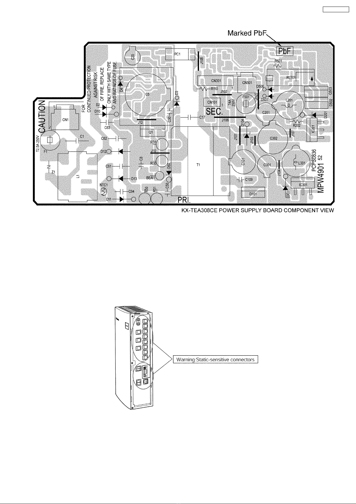
21.6. POWER SUPPLY 86
21.7. MEMO 87
22 PRINTED CIRCUIT BOARD (KX-TEA308CE) 88
22.1. MAIN BOARD 88
22.2. CO BOARD 90
22.3. POWER SUPPLY 92
23 KX-TE82460X (2-PORT DOORPHONE CARD) 93
23.1. HOW TO RECOGNIZE THAT Pb FREE SOLDER IS
USED 94
CONTENTS
Page Page
2
KX-TEA308CE

23.2. LOCATION OF OPTIONAL CARDS 95
23.3. DOORPHONE/DOOROPENER CARD BLOCK DIAGRAM
96
23.4. EXPLANATION OF BLOCK DIAGRAM/CIRCUIT
OPERATIONS 96
23.5. TROUBLESHOOTING GUIDE 97
23.6. IC DATA 98
23.7. TERMINAL GUIDE OF ICS, TRANSISTORS AND
DIODES 100
23.8. ACCESSORIES AND PACKING MATERIALS 100
23.9. REPLACEMENT PARTS LIST (KX-TE82460X) 101
23.10. FOR THE SCHEMATIC DIAGRAM 103
23.11. SCHEMATIC DIAGRAM (KX-TE82460X) 104
23.12. PRINTED CIRCUIT BOARD (KX-TE82460X) 106
24 KX-TE82492X (2-CHANNEL VOICE MESSAGE CARD) 107
24.1. HOW TO RECOGNIZE THAT Pb FREE SOLDER IS
USED 108
24.2. LOCATION OF OPTIONAL CARDS 109
24.3. BLOCK DIAGRAM 110
24.4. CIRCUIT OPERATIONS 111
24.5. TROUBLESHOOTING GUIDE 112
24.6. IC DATA 114
24.7. TERMINAL GUIDE OF ICS, TRANSISTORS AND
DIODES 115
24.8. ACCESSORIES AND PACKING MATERIALS 115
24.9. REPLACEMENT PARTS LIST (KX-TE82492X) 116
24.10. FOR THE SCHEMATIC DIAGRAM 117
24.11. SCHEMATIC DIAGRAM (KX-TE82492X) 118
24.12. PRINTED CIRCUIT BOARD (KX-TE82492X) 120
25 KX-TE82493X (3-PORT CALLER ID CARD) 121
25.1. HOW TO RECOGNIZE THAT Pb FREE SOLDER IS
USED 122
25.2. LOCATION OF OPTIONAL CARDS 123
25.3. BLOCK DIAGRAM 124
25.4. CIRCUIT OPERATIONS 124
25.5. TROUBLESHOOTING GUIDE 125
25.6. IC DATA 126
25.7. TERMINAL GUIDE OF ICS, TRANSISTORS AND
DIODES 128
25.8. ACCESSORIES AND PACKING MATERIALS 128
25.9. REPLACEMENT PARTS LIST (KX-TE82493X) 129
25.10. FOR THE SCHEMATIC DIAGRAM 131
25.11. SCHEMATIC DIAGRAM (KX-TE82493X) 132
25.12. PRINTED CIRCUIT BOARD (KX-TE82493X) 134
26 KX-A227X (BACK-UP BATTERY CABLE) 135
26.1. ACCESSORIES AND PACKING MATERIALS 136
26.2. REPLACEMENT PARTS LIST (KX-A227X) 137
3
KX-TEA308CE

1 ABOUT LEAD FREE SOLDER (PbF: Pb free)
Note:
In the information below, Pb, the symbol for lead in the periodic table of elements, will refer to standard solder or solder that
contains lead.
We will use PbF solder when discussing the lead free solder used in our manufacturing process which is made from Tin, (Sn),
Silver, (Ag), and Copper, (Cu).
This model, and others like it, manufactured using lead free solder will have PbF stamped on the PCB. For service and repair
work we suggest using the same type of solder although, with some precautions, standard Pb solder can also be used.
Caution
•
• •
• PbF solder has a melting point that is 50° ~ 70° F, (30° ~ 40°C) higher than Pb solder. Please use a soldering iron with
temperature control and adjust it to 700° ± 20° F, (370° ± 10°C). In case of using high temperature soldering iron, please
be careful not to heat too long.
•
• •
• PbF solder will tend to splash if it is heated much higher than its melting point, approximately 1100°F, (600°C).
•
• •
• If you must use Pb solder on a PCB manufactured using PbF solder, remove as much of the original PbF solder as possible
and be sure that any remaining is melted prior to applying the Pb solder.
•
• •
• When applying PbF solder to double layered boards, please check the component side for excess which may flow onto the
opposite side (See figure, below).
1.1. SUGGESTED PbF SOLDER
There are several types of PbF solder available commercially. While this product is manufactured using Tin, Silver, and Copper,
(Sn+Ag+Cu), you can also use Tin and Copper, (Sn+Cu), or Tin, Zinc, and Bismuth, (Sn+Zn+Bi). Please check the
manufacturer’s specific instructions for the melting points of their products and any precautions for using their product with other
materials.
The following lead free (PbF) solder wire sizes are recommended for service of this product: 0.3mm, 0.6mm and 1.0mm.
4
KX-TEA308CE

1.2. HOW TO RECOGNIZE THAT Pb FREE SOLDER IS USED
5
KX-TEA308CE

6
KX-TEA308CE

2 FOR SERVICE TECHNICIANS
ICs and LSIs are vulnerable to static electricity.
When repairing, the following precautions will help prevent recurring malfunctions.
1. Cover the plastic parts boxes with aluminum foil.
2. Ground the soldering irons.
3. Use a conductive mat on the worktable.
4. Do not touch IC or LSI pins with bare fingers.
7
KX-TEA308CE

3 CAUTION
3.1. SAFETY PRECAUTIONS
1. Before servicing, unplug the power cord to prevent an electric shock.
2. When replacing parts, use only the manufacturer´s recommended components for safety.
3. Check the condition of the power cord. Replace if wear or damage is evident.
4. After servicing, be sure to restore the lead dress, insulation barriers, insulation papers, shields, etc.
5. Before returning the serviced equipment to the customer, be sure to perform the following insulation resistance test to prevent
the customer from being exposed to shock hazards.
3.2. INSULATION RESISTANCE TEST
1. Unplug the power cord and short the two prongs of the plug with a jumper wire.
2. Turn on the power switch.
3. Measure the resistance value with ohmmeter between the jumpers AC plug and each exposed metal cabinet part, such as
screw threads, control shafts, handle brackets, etc.
Note:
Some exposed parts may be isolated from the chassis by design. These will read infinity.
4. If the measurement is outside the specified limits, there is a possibility of shock hazard. The equipment should be repaired and
rechecked before it is returned to the customer.
3.3. BATTERY CAUTION
1. Danger of explosion if battery is incorrectly replaced. Replace only with the same or equivalent type recommended by the
manufacturer. Dispose of used batteries according to the manufacturer’s Instructions.
2. The lithium battery is a critical component (type No.CR23541). Please observe for the proper polarity and the exact location
when replacing it and soldering the replacement lithium battery in.
3.4. CAUTION
The power socket wall outlet should be located near this equipment and be easily accessible.
8
KX-TEA308CE

4 SPECIFICATIONS
4.1. GENERAL DESCRIPTION
Control Bus Original bus (16-bit, 24 MHz)
Switching Space Division CMOS Crosspoint Switch
Power Input 100 V AC to 240 V AC, 0.8A to 0.4A, 50 Hz/60Hz
External Battery +24 V DC (+12 V DC x 2)
Maximum Power Failure Tolerance 300 ms (without using backup batteries)
Memory Backup Duration 7 years
Dialling Outside (CO) Line Pulse (10 pps, 20 pps) or Tone (DTMF)
Extension Pulse (10 pps, 20 pps) or Tone (DTMF)
Intercom Path 3
Mode Conversion Pulse-DTMF
Ring Frequency 20 Hz/25 Hz (selectable)
Operating Environment Temperature 0°Cto40°C
Humidity 10 % to 90 % (non-condensing)
Conference Call Outside (CO) Line 2
Music on Hold (MOH) 1 port
Selectable MOH: Internal/External/Tone
Paging Internal 1
Extension 1 port
Serial Interface Port RS-232C 1
USB 1.1 1
Extension Connection Cable SLT 1 pair wire (T, R)
PT 2-pair wire (T, R, H, L)
DSS Console 1-pair wire (H, L)
Dimension 249 mm (W) x 316 mm (H) x 73 mm (D)
Weight (when fully expanded) Approx. 1.8 kg
4.2. CHARACTERISTICS
Terminal Equipment Loop Limit PT 40 Ω
SLT 600 Ωincluding set
Doorphone 20 Ω
Minimum Leakage Resistance 15000 Ωminimum
Maximum Number of Extension
Instruments per Line
1 PT or SLT in standard connection
1 PT and 1 SLT in parallel connection
Ring Voltage 65 Vrms at 20 Hz/25 Hz depending on the ringing load
Outside (CO) Line Loop Limit 1600 Ωmaximum
Hookswitch Flash/Recall Timing Range 24 ms-2032 ms
Door Opener Current Limit 30 V DC/30 V AC, 3 A maximum
Paging Terminal Impedance 600 Ω
MOH Terminal Impedance 10000 Ω
4.3. SYSTEM CAPACITY
4.3.1. System Capacity
KX-TEA308
Basic System Outside (CO) line 3
Extensions for PT/SLT 8
9
KX-TEA308CE

4.3.2. Maximum Cards Terminal Equipment
ltem KX-TEA308
PT 8
SLT 8
2-Port Doorphone Card 1
3-Port Caller ID Card 1
2-Channel Voice Message Card 1
Doorphone 2
Door Opener 2
Pager 1
Music on Hold (MOH) 1
DSS Console 2
4.3.3. System Data
ltem Max. Quantity
Operator 1
System Speed Dialling 100
One-touch Dialling 24 per extension (PT)
Personal Speed Dialling 10 per extension
Call Park Area 10
Absent Message 6
Toll Restriction (TRS) COS 5
Extension Group 8
Message Waiting 8 per extension
Message for Built-in Voice Message 125 messages (total 60 minutes)
5 SYSTEM OVERVIEW
5.1. SYSTEM COMPONENTS
Model Description
Main Unit KX-TEA308CE Advances Hybrid System: 3 Outside (CO) Line, 8 Hybrid Extentions
Optional Service Cards KX-TE82460X
KX-TE82492X
KX-TE82493X
2-Port Doorphone Card
2-Channel Voice Message Card
3-Port Caller ID Card
Proprietary Equipment KX-T30865
KX-A227X
Doorphone
Backup Battery Cable
10
KX-TEA308CE

5.2. SYSTEM CONNECTION DIAGRAM
•
• •
• Connect a display-equipped proprietary telephone (PT) to extension jack 01, as this extension is automatically designated as
the manager extension.
11
KX-TEA308CE

6 NAMES AND LOCATIONS
7 CONNECTION
7.1. SERIAL INTERFACE CONNECTION
12
KX-TEA308CE

8 DISASSEMBLY INSTRUCTIONS
8.1. DISASSEMBLY INSTRUCTION
1. Pull the slide button (arrow 1) to the right and, holding it, slide the
cable cover upwards (arrow 2).
2. Then turn the cable cover slightly to remove it.
3. Remove the three screws (A).
4. Holding the protrusions on both sides of the front cover, swing the
cover open.
5. Holding the front cover open at about a 45° angle, remove the front
cover by pushing it in the direction of the arrow as shown on the right.
13
KX-TEA308CE

5. Remove the 1 screws (A).
6. Remove the power supply board cover.
7. Pull out the 4 connectors.
8. Remove the 2 screw (B) and 1 screw (A).
9. Remove the power supply board.
10. Remove the 2 screw (B).
11. Remove the CO board.
12. Pull out the 1 connector.
13. Remove the 2 screws (A) and 1 screw (B).
14. Remove the main board.
Procedure:
•
• •
• Insert the SW CABLE into AC POWER SWICH.
Caution:
•
• •
• Be sure each colored wire is inserted to the correct lug (very important).
14
KX-TEA308CE

9 BLOCK DIAGRAM
9.1. SYSTEM BLOCK DIAGRAM
15
KX-TEA308CE

9.2. POWER BLOCK DIAGRAM
9.3. KX-TEA308CE MAIN BLOCK DIAGRAM
KX-TEA308CE 1AP BLOCK DIAGRAM
Host i/f
Q1-4,TOE1,2,STD1,2
TONE
25Hz
CROSS
POINT
ROM
SRAM
DTMFR(1,2)
(For EXT)
PIO
ASIC
BELL
TONE
(I/O)HOOK1-8,BELL1-8
620,440,350Hz
CO CID
CONNECTOR
D-Sub
POWER UNIT
CONNECTOR
USB
CO1-3
EXT1-8
I/O,DTMFG
BGM
PAGE
CO
(2AP)
Card
CONNECTOR
ASIC
8086
DSP
P I O
APT i/f
BV Card
CONNECTOR
TAM1-2,TONE
(APT i/f)PRX,PTX,PTXE1-3
(UART)RXD,TXD
EXT1
EXT2
EXT3
EXT4
EXT5
EXT6
EXT7
EXT8
Ringer
Circuit
Door Phone
Door Opener
CONNECTOR
DOOR1,2
Int CID(FSK,DTMF)
OGM,Modem
CN708
CN707
CN701
CN706
CN710
CN704
CN703
IC601
IC602
IC603
IC705
IC704
IC700
IC7, IC8
IC606, IC607
16
KX-TEA308CE

9.4. KX-TEA308CE CO BLOCK DIAGRAM
9.5. KX-TEA308CE POWER SUPPLY UNIT BLOCK DIAGRAM
KX-TEA308CE POWER SUPPLY UNIT BLOCK DIAGRAM
AC IN
L
FUSE
Surge
Protector
Noise
Control
Over
Current
Detection
Circuit
Filter
Rectifier
Primary Secondary
&
Smoother
Rectifier Voltage
Detection
&
Smoother
N
FG
Battery +24
V
+27V
+15V
GND
GND
SW
Back-up
Adaptor
DC-DC
Converter
+3.3V
DC-DC
Converter
CN1
F1
Z1 L1
D10 ~ D13
C5
IC1
PC1
Q1
R30, R31
D101, C101
IC101
RL501
Q503
IC201
IC301
17
KX-TEA308CE

10 EXPLANATION OF BLOCK DIAGRAM
10.1. MAIN UNIT (KX-TEA308CE)
10.1.1. Power Supply Circuit
This power supply unit is a switching power supply. Power supply unit supplies DC voltage (+27V,+15V,3.3V) to main board and
other optional cards. And this unit has an adaptor circuit to back up battery.
10.1.2. COL Interface Circuit
There are the interface circuits linking the CO line (CO1 -CO3) and the cross point circuit section.
10.1.3. Cross Point Circuit
This is a space division switching system for connecting the following:
The eight extension circuits with the three CO, DTMF generator, DTMF receiver, INT-CALL ID, MODEM, OGM, BV, paging, music
on hold, tone etc.
It is composed of 3 C-MOS IC´s. (8 X 16 matrix: 1pcs and 4 X 8 matrix: 2pce).
10.1.4. Intercom Circuit
This is the interface circuit of the single line telephone, and it is composed of 8 intercom circuit (ICM1-8).
10.1.5. Power Failure Through Call Switching Circuit
There is one power failure transfer circuit (CO1-EXT101).
10.1.6. Data Communication Circuit
The APT i/f module which performs communication with a private telephone machine is built in ASIC.
10.1.7. Control Circuit
A control block consists of CPU (compatibility with Intel 8086) (IC700), Flash ROM (8Mbit) (IC705) and SRAM (4Mbit) (IC704).
RTC, Timer, DMAC, USB Controller, WDT, INTC, UART, General Purpose I/O ports, APT i/f and DSP are built into CPU chip.
General purpose I/O block is composed by discrete parts (IC7, IC8) and the I/P port in CPU.
IC7 and IC8 control extension, and the I/O ports in CPU control the COL chiefly.
In order to maintain time, system data and others, RTC (Real Time Clock) in CPU and SRAM are backed up with the lithium battery.
10.1.8. Tone Generator Circuit
The rectangle wave generated by the timer of CPU is changed into sine wave with a low pass filter, and various tones are
generated.
10.1.9. DTMF Generator Circuit
DTMF (Dial Tone Multi Frequency) generator is used for dispatch to outside line, and communication with the voice mail connected
to the extension.
10.1.10. DTMF Receiver Circuit
The circuit that receives the Dial Tone Multi Frequency by which extension dispatch is carried out with the DTMF receiver
connected to the crossing point.
10.1.11. Int Call ID Circuit
FSK/DTMF generated by DSP in CPU are connected even to a crossing point through AMP. The circuit which sends out a CALLID
signal to the telephone connected to an extension by connecting the line of INT-CALL-ID with arbitrary extensions.
10.1.12. Modem Circuit
The MODEM signal generated by DSP in CPU is connected even to a crossing point through AMP.
The circuit, which connects the line of MODEM with arbitrary outside line, and enables MODEM communication with outside line.
10.1.13. USB Circuit
The circuit which makes communication possible by PC and 1.1 standards by the USB controller in CPU.
18
KX-TEA308CE

10.1.14. OGM Circuit
The 4M Serial Flash ROM is connected to CPU by the memory controller in DSP (in CPU).
A maximum of 3-minute storing of OGM is possible to a serial flash ROM.
10.1.15. Ring Signal Generator Circuit
This section generates the ring signal for the single line telephone. A 20/25Hz square wave is generated by the CPU timer and sent
to low pass filter and the Ring signal is amplified by BELL amplifier circuit, and then passed it through the ringing signal switching
relay to the single line telephone.
10.1.16. SMDR Interface Circuit
This is the RS232C interface port. When the port is connected to a printer. The port can be used to output the SMDR feature
recording messages and the contents of the system program.
10.1.17. Door Phone Interface
An doorphone card interface consists of two intercom paths connected to a crossing point, and address data and CS signals.
10.1.18. Call ID Interface
A CALLID card interface consists of three CALLID signal lines from outside line, and address data and CS signal.
10.1.19. BV Interface
BV card interface consists of two BV telephone call paths connected to a crossing point, and address data and CS signals.
19
KX-TEA308CE

11 CIRCUIT OPERATION
11.1. POWER SUPPY CIRCUIT
11.1.1. The function of the power unit are listed below
AC-DC Inverter Function This function isolates and converts the AC input voltage to DC
input and output of DC27V.
DC-DC Converter Function This function outputs DC+15V and 3.3V from the inputted
DC27V.
Battery Back Up Adaptor Function This function connects battery and service unit without battery
adaptor, only needs a cable connected to the battery and
service unit.
20
KX-TEA308CE
This manual suits for next models
4
Table of contents
Other Panasonic Heater manuals

Panasonic
Panasonic FV-07VFH3 User manual

Panasonic
Panasonic FV-0511VH1 User manual

Panasonic
Panasonic FY-2509U1 User manual

Panasonic
Panasonic FV-07VFH3 User manual

Panasonic
Panasonic Basic Series User manual

Panasonic
Panasonic FV-0511VHL1 User manual

Panasonic
Panasonic FV-11VH2 User manual

Panasonic
Panasonic FY-08ESN User manual

Panasonic
Panasonic FV-0511VH1 User manual

Panasonic
Panasonic FY-3009U1 User manual