Philips pm2521 User manual

Automatic Multimeter
PM2521
Service Manual
9499 475 01911
820407

Automatic Multimeter
PM2521
Service Manual
9499 475 01911
820407
IMPORTANT
This service manual is based on instruments with aserial number DM 01 1145 and onwards.
In chapter 11, modifications to the PM2521, an overview is given of modifications in the earlier instruments.
PHILIPS

02
IMPORTANT
In correspondence concerning this instrument, please quote the type number and serial number as given on
the type plate.
NOTE: The design of this instrument is subject to continuous development and improvement.
Therefore the instrument may not exactly comply with the information in the manual.
WICHTIG
Bei Schriftwechsel iiber dieses Gerat wird gebeten, die genaue Typenbezeichnung und die Geratenummer
anzugeben. Diese befinden sich auf dem Leistungsschild.
BEMERKUNG: Die Konstruktion und Schaltung dieses Gerats wird standig weiterentwickelt und verbessert.
Deswegen kann dieses Gerat von den in dieser Anieitung stehenden Angaben abweichen.
IMPORTANT
Dans votre correspondence se rapportant acet appareil, veuillez indiquer le numero de type et le numero de
serie qui sont marques sur la plaqUette de caracteristiques.
REMAROUES: Cet appareii est i'objet de developpements et ameliorations continuels. En consequence, certains
details mineurs peuvent differer des informations donnees dans ia presente notice d'emploi et
d'entretien.
©N.V. PHILIPS' GLOEILAMPENFABRIEKEN -EINDHOVEN -THE NETHERLANDS -1982
PRINTED IN THE NETHERLANDS

03
CONTENTS Page
1. CIRCUIT DESCRIPTION 1
1.1. General 1
1.2. Survey of main sections 1
1.2.1. Analog section 1
1.2.2. Control section 6
1.2.3. Display section 6
1.3. Functional description 6
1.3.1. General 6
1.3.2. Analog section (standard measurements) 7
1. 3.2.1. Direct voltage measurements 7
1.3. 2. 2. Alternating voltage measurements 8
1.3.2.3. Direct current measurements 9
1.3.2.4. Alternating current measurements 9
1.3.2. 5. Resistance measurements 10
1.3.2. 6. Diode measurements 11
1.3.2.7. Temperature measurements 11
1.3.3. Analog section (extended measurements) 12
1. 3.3.1. Frequency measurements 12
1.3.3.2. Time measurements 13
1. 3.3.3. Trigger measurements 13
1.3.4. Analog section (multifunction circuits) 14
1. 3.4.1. R.M.S. convertor 14
1.3.4. 2. Impedance convertor 14
1.3.4. 3. Active filter 15
1. 3.4.4. Analog-to-Digital convertor 15
1.3.5. Control section 17
1.3. 5.1. Microprocessor 8035 17
1.3.5. 2. Interrupt controller 21
1.3.5. 3. Counter 22
1. 3.5.4. Analog control 22
1.3.5. 5. ROM's and Address/Data decoding 23
1.3.6. Display section 23
1.4. Detailed circuit description 26
1.4.1. Measuring sequence 26
1.4. 1.1. Initialisation 27
1.4. 1.2. Internal test and adjust routine 28
1.4. 1.3. Set up routine 31
1.4. 1.4. Measurement routine 31
1.4. 1.5. Calculation routine 32
1.4. 1.6. Display output routine 32
1.4.2. Analog section (standard measurements) 33
1.4.2.1. Direct voltage measurements 33
1.4.2.2. Alternating voltage measurements 34
1.4.2.3. Direct current measurements 35
1.4.2.4. Alternating current measurements 36
1.4.2.5. Resistance measurements 37
1.4.2. 6. Diode measurements 38
1.4.2.7. Temperature measurements 38

04
1.4.3. Analog section (extended measurements) 39
1.4.3.1. Frequency measurements 39
1.4.3.2. Time measurements 40
1.4.3.3. Trigger measurements 40
1.4.4. Analog section (multifunction measurements) 41
1.4.4.1. R.M.S. convertor 41
1.4.4.2. Impedance convertor 42
1.4.4.3. Active filter 43
1.4.4.4. Analog-to-Digital convertor 44
1.4.5. Control section 45
1.4.5.1. Interrupt controller 45
1.4. 5.2. Counter and Input control 47
1.4.5.3. Analog control 48
1.4.5.4. ROM circuit and Address/Data decoding 54
1.4.6. Display section 56
1.4.7. Power supply 56

2.
ACCESS 57
2.1. Dismantling the PIVI2521 57
2.1 .1 .Removing the top cover 57
2.1.2. Removing the bottom cover 57
2.1.3. Removing the front assembly 57
2.2. Replacing parts 58
2.2.1. Liquid crystal display, display unit N3, interconnection rubber or function knob ... 58
2.2.2. Function switch 58
2.2.3. Thermal fuse 58
3. CHECKING AND ADJUSTING 62
3.1. DC ranges 63
3.2. AC ranges 65
3.3. Trigger level ranges 66
3.4. Current ranges 68
3.5. Resistance ranges 68
3.6. Temperature ranges 69
3.7. Frequency ranges 69
3.8. Time ranges 70
4. FAULT-FINDING 71
4.1. General 71
4.1.1. Service hints 71
4.1.2. Fault-finding procedure 71
4.1.3. Fault-finding with the signature analyser 71
4.2. Fault-finding flow-charts 72
4.2.1. Basic check 72
4.2.2. Function part 73
4.2.3. V.77 part 74
4.2.4. V~part 74
4.2.5. Trigger level part 76
4.2.6. A.r: and A~part 78
4.2.7. fZ part 79
4.2.8. Analog part 80
4.2.9. ADC part 81
4.2.10. Digital part 82
4.2.11. Free-run 84
4.2.12. Display part 86
4.2.13. Power supply check 88

06
5. PARTS LIST 89
5.1. Top cover assembly 89
5.2. Bottom cover assembly 89
5.3. Front assembly 89
5.4. Switch assembly 89
5.5. Printed circuit board 90
5.5.1. Miscellaneous 90
5.5.2. Resistors 91
5.5.3. Capacitors 94
5.5.4. Semi-conductors 96
5.5.5. Integrated circuits 98
6. CIRCUIT DIAGRAMS AND P.C.B. LAY-OUT 99
7. MODIFICATIONS TO THE PM2521 115
7.1. Modifications to circuit diagrams and p.c.b. lay-outs 115
7.2. Modifications to components 120
7.3. Modifications to the adjusting procedure 120
8. COMPONENT DATA 121
8.1. Semi-conductors 121
8.2. LOCMOS circuits (HEF) 122
8.3. OQ circuits 127
8.4. Display interface circuits 133
8.5. Operational amplifiers 137
8.6. Low power Schottky circuits (LS) 139
8.7. Memory and microprocessor 143
8.8. Resistors 146


6
Fig. 1. Basic built-up of PM2521
CONTROL SECTION DISPLAY SECTION
1.2.2.
Control Section
The control section comprises the following circuit elements:
—The interrupt controller
The inputs for the interrupt controller are the mode switches and the trigger level circuit output
(timer part)
—The counter with its input control
The inputs for the counter circuit are;
—The ADC output
—The trigger level circuit output (counter part)
The input control is directed from the microcomputer
—The ROM with address/data decoding
—The microcomputer 8035
—The function selector with decoding
—The mode switches
—The relay/FET switch control
1.2.3. Display section
The display section consists of:
—The display interface circuit
—The 5-digit liquid-crystal display
1.3. FUNCTIONAL DESCRIPTION
1.3.1. General
in common with most microcomputer-based measuring instruments, the Automatic Multimeter PM2521 is
designed around the microcomputer integrated circuit -an 8035 with a4K external ROM. The 8035 comprises
amicroprocessor with an internal 64-byte RAM, one true 8-bit bidirectional port and two quasi-bidirectional
ports.
In conjunction with the 4K ROM, the pP controls the timing and measuring functions of the instrument.
It also provides the reading of the display.
In the analog section, all the inputs are converted into d.c. signals, attenuated as necessary under pP control
and supplied to the ADC.
The ADC converts these d.c. analog representations of the input signals into digital logic signals suitable for the
pP.
The measuring sequence from analog section to control and display sections is briefly outlined in the flow-
chart, Fig. 3.
Fig. 2. Biockdiagram PM2521

07
LIST OF FIGURES
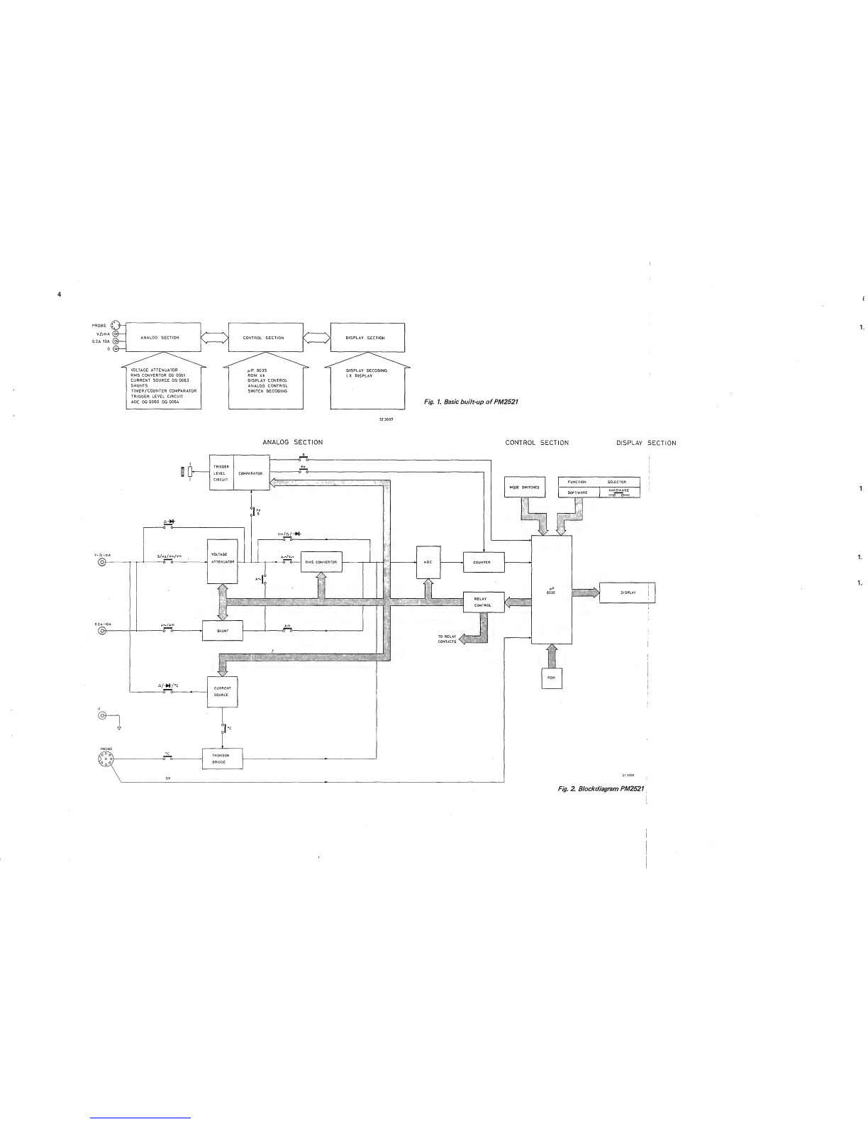
Fig. 1. Basic build-up of PM2521 4
Fig. 2. Block diagram PIVI2521 4
Fig. 3. Measurement flow-chart ... 7
Fig. 4. DC attenuator .1 8
Fig. 5. AC attenuator 8
Fig. 6. Basic 1-V convertor 9
Fig. 7. measurements 10
Fig. 8. Thomson bridge 11
Fig. 9. Block diagram -frequency measurements 12
Fig. 10. Normal trigger mode 13
Fig. 11. Special trigger mode 13
Fig. 12. Basic V-l convertor 14
Fig. 13. Low-pass active filter 15
Fig. 14. Switching part ADC 15
Fig. 15. Basic functional blocks of 8035/mP 17
Fig. 16. Pin allocation and functions of 8035/xP 19
Fig. 17. Mode switch interrupts 21
Fig. 18. Block diagram of the control section 24
Fig. 19. Measuring sequence 26
Fig. 20. Calibration routine 29
Fig. 21. Flow-chart internal test and adjust routine 28
Fig. 22. Flow-chart display output routine 32
Fig. 23. DC attenuator details 33
Fig. 24. AC attenuator details 34
Fig. 25. I-V convertor 35
Fig. 26. mesusrements details 37
Fig. 27. Temperature bridge 38
Fig. 28. Frequency measurements 39
Fig. 29. R.M.S. convertor 41
Fig. 30. Impedance convertor 42
Fig. 31. Active filter 43
Fig. 32. V-l convertor 44
Fig. 33. Interrupt controller 45
Fig. 34. Counter input control 47
Fig. 35. Counter 48
Fig. 36. Switch decoding 49
Fig. 37. Relay/FET control 51
Fig. 38. Address decoding 54
Fig. 39. Memory 55
Fig. 40. Display interface 56
Fig. 41 .Removing the top cover 60
Fig. 42. Removing the bottom cover and front 60
Fig. 43. Removing the front 60
Fig. 44. Front assembly 60
Fig. 45. Removing the thermal fuse 60
Fig. 45a. Removing the thermal fuse 60
Fig. 46. Adjusting elements 61
Fig. 47. Waveforms V~ part 74
Fig. 48. Waveforms trigger-level part 77
Fig. 49. Waveform, analog part 80
Fig. 50. Waveform, ADC part 81

08
Fig. 51. Waveforms, digital part 82
Fig. 52. Waveforms, free-run 85
Fig. 53. Switch for high current ranges 90
Fig. 54. Switch p.c.b. iay-out, front view 99
Fig. 55. Switch p.c.b. lay-out, rear view 99
Fig. 56. Display p.c.b. lay-out, component side 100
Fig. 57. Display p.c.b. lay-out, conductor side 100
Fig. 58. Adapting the mains transformer 101
Fig. 59. Main p.c.b. lay-out, component side 102
Fig. 60. Main p.c.b. lay-out, conductor side 103
Fig. 61 .Additional components on conductor side of main p.c.b 104
Fig. 62. Power supply circuit diagram 105
Fig. 63. Analog section circuit diagram 110
Fig. 64. Digital section circuit diagram Ill
Fig. 65. Modifications in active filter 115
Fig. 66. Modifications in current source 116
Fig. 67. Main p.c.b. lay-out, component side former version 117
Fig. 68. Main p.c.b. lay-out, conductor side former version 118
Fig. 69. Additional components on conductor side of main p.c.b 119

7
Fig. 3. Measurement flow-chart
The various circuit functions are now described together with explanations of basic principles as necessary.
1.3.2. Analog section (standard measurements)
1.3.2. 1. Direct voltage measurements
The unknown voltage to be measured is passed to the a.c./d.c. voltage attenuator where by means of resistors
switched by relay contacts controlled from the n?, the attenuation factor is changed from the basic 2V range
to give 20V, 200V and 2000V ranges. The 200mV range uses the 2V range attenuator position, but the ADC
is switched to the lOOmV position to give the necessary xIO gain factor.
From the voltage attenuator the signal is fed to an active filter, which stabilises the voltage passed to the ADC.
The ADC converts this analog voltage into digital form for the /iP to measure.

10
1.3.2. 5. Resistance measurements
The unknown resistance is connected between the V-fi-mA and 0input terminals and supplied internally
with aconstant-current source dependent on the range selected. This current results in apotential difference
across the resistor which (by Ohm's Law) is proportional to the resistance value. The resulting voltage signal
is applied as for Vmeasurements to the voltage attenuator, the active filter and the ADC.
The circuit functions as shown in Fig. 7.
Aknown constant current supplied by the programmable current source A401 (000063) flows through
the unknown resistor Rx.
There are three basic ranges:
^2 200
k^2 220 200
M^2 220
Depending on the range selected (manual or automatic selection), the currents are determined by the signals
RNGC, RNGD and RNGE:
Irx RNGC RNGD RNGE RANGE Vx INDICATION
1mA -10V -10V OV 200 n-0,2V 200.00 n
1mA -10V -10V ov 2kfi -2V 2.0000kf2
100/tA -10V -10V -10V 20kl2 -2V 20.000kf2
10m Aov -10V -10V 200kfi -2V 200.00kn
lM A-10V ov -10V 2Mn -2V 2.0000M12
lOOn Aov ov -10V 20IVir2 -2V 20.000Mr2
With respect to
Fig. 7. Qj measurements
In practice, the internal resistance of the ADC (10IViJ2) also draws asmall amount of current, but, this is com-
pensated by an equivalent current through the compensation amplifier circuit.

11
1. 3.2.6. Diode meauserements
The measurement of diodes and semiconductor junctions is performed in the same way as for resistance
measurements in the 2kfZ range.
The value displayed is the equivalent of the voltage measured in the forward or reverse direction across the
diode junction in the 2V range; i.e. the constant current multiplied by the diode resistance.
For diode measurements the constant current derived from the OQ0063 is 1mA (see previous section).
1. 3.2.7. Temperature measurements
For temperature measurements, aconstant current from the A401 current source flows through the resistance
element of the temperature probe to produce avoltage drop across it. This resistance is connected as one of
the ratio arms of aThomson bridge. The voltage drop is an indication of the temperature of the Pt-100 probe
(—50°C ... +200°C) and is applied to the ADC for measurement.
circuit element principles:
Thomson bridge: The temperature probe (resistance thermometer) is included in one arm of a
balanced resistive 4-wire bridge. The balancing potentiometer is R708; the slider
connects the output of the bridge directly to the ADC.
In this configuration, the small resistances of the connecting leads are counter-
acted; they are either in series with the current source or in series with the much
higher resistance arms of the bridge, so their effect is negligible.
3
1
BU4
C.
AV' =SMALL RESISTANCES OF PROBE LEADS
ST3364
Fig. 8. Thomson bridge

12
1.3.3. Analog section (extended measurements).
1.3.3. 1. Frequency measurements
The unknown frequency source to be measured is applied to the Vand 0input terminals. After suitable
attenuation as necessary in the a.c. voltage attenuator and impedance conversion (to match the low-impe-
dance comparator) the signal is fed to one input of the comparator A502.
The trigger level input selected by the front-panel thumbwheel control is applied via an impedance convertor
to the other input of the comparator.
The trigger level is set to avalue lower than the amplitude of the signal to be measured. During counting,
each time the amplitude of the signal from the input exceeds the selected trigger level, the compartor gives
an output pulse to the counter. The internal counter of the IIP is also used as an overflow counter for
frequency measurements.
Triggering is also possible on the negative-going pulses of asignal by using the +/— switch to reverse the
polarity of the trigger level.
+
ST3365
811127
Fig. 9. Block diagram-frequency measurements

13
1.3.3. 2. Time measurements
Time measurements of signals are determined in conjunction with the trigger level function in asimilar way to
frequency measurements.
The input signal is applied via the voltage attenuator to one input of the comparator A502. The selected
trigger level is applied to the other input.
When the amplitude of the signal exceeds that of the selected trigger level, an output pulse from the com-
parator is applied direct to the microprocessor.
Two trigger modes are possible for the time measurement function:
In the normal trigger mode, signals that are higher or lower than the circuit zero (0 terminal of PM2521 )can
be triggered with the -i- or —trigger level respectively.
•(-TRIGGER
LEVEL 0
TRIGGER POINTS (+-(1 TRIGGER POINTS! )
ST 301
6
S20226
Fig. 10. Normal trigger mode
In the special trigger mode, using Data Hold Probe PM9263, the PM2521 triggers in the -i- level mode on
positive and negative crossings of the trigger level.
Conversely, in the —level mode it triggers on negative and positive crossings of the trigger level.
•(TRIGGER 1
LEVEL O'
TRIGGER POINTS!-!--) TRIGGER points!—(-1
A1\
°-i:i1'p:
A1V
TRIGGER
LEVEL
ST 3016
820226
Fig. 11. Special trigger mode
1. 3.3.3. Trigger measurements
In addition to time and frequency applications, the trigger level function permits other selective measurements
to be made.
To measure the peak voltage of an input signal the front-panel trigger level control is rotated until the GATE
indicator display is triggered either on or off. At this switch-over point the voltage indicated on the display
represents the amplitude or peak voltage of the input signal.

14
1.3.4. Analog section (multifunction circuits)
1. 3.4.1. R.M.S. convertor
Basically, the circuit is an a.c. to d.c. convertor built around the OQ0061 1C, which consists of three parts:
—Avoltage-to-current convertor with two selectable input ranges
—Acurrent rectifier with offset cancellation
—Alog-antilog calculating R.M.S circuit
Circuit element principles:
As shown in Fig. 12, the basic V-to-l convertor consists of two input devices T1, T2 fed from two equal
current sources and aconversion resistor R. The voltage V(= Vini -Vin2) developed across Rgives acurrent
I=Vthrough R. This current increases the emitter current of T1 and decreases the emitter current of T2.
This results in collector output currents of I-t AIfor T1 and I—AIfor T2.
Then the current is rectified to give asignal proportional to the R.M.S. value of the input signal Vin.
In practice, amore complex circuit is used to compensate for the differences in base-emitter currents.
The two equal currents Iare derived from acurrent bias source.
For electronic range selection, two V-to-l convertors are used with common input and output devices but with
separate conversion resistors.
The selection circuit for these has aselection input and aselection reference input that can be connected to
various d.c. levels to give more control flexibility.
ST3Jb6
811126
Fig. 12. Basic V-to-i convertor
1. 3.4.2. impedance convertor
The impedance convertor converts the high input impedance signal to alow impedance to match the input
of the R.M.S. convertor.
This impedance matching also applies to the input of the trigger level comparator, as otherwise it would draw
current from the signal.

15
1. 3.4.3. Active filter
Filters placed in feedback loops around an amplifier stage are referred to as active filters. They have sharper
transition between the pass-band and stop-band than their passive counterparts, inductors are not needed,
and small signals are not further attenuated.
In this application, good filtering is necessary especially when measuring small a.c. signals.
In this circuit, the basic active filter elements are as shown:
Fig. 13. Low-pass active filter
ST3367
820503
In the PM2521 ,the track shielding network on the filter output keeps the two signal lines that are connected
to it at the same potential; i.e. prevents tracking across the p.c.b. insulation.
I.3.4.4. Analog-to-digital Convertor
The ADC converts the analog signal into adigital signal by the 'delta-modulation' principle.
Basically, the delta-modulation ADC counts the difference in the time taken to charge and to discharge a
capacitor about afixed level, over afixed period of time.
The number of charge/discharge cycles within this fixed time depends on the charge/discharge current which
is made proportional to the unknown input voltage to the ADC.
Therefore, the number of pulses counted within afixed measuring period is proportional to the unknown
voltage V^.
Circuit principles:
The capacitor is charged by aconstant reference current added to the constant current derived from Vto
give (I ref -I- AI). ^
The capacitor is discharged by the constant reference current minus the constant current derived from V
to give (I ref -AI).
Each value of has acertain number of charge/discharge cycles within the fixed period of aspecific number
of clock-pulses counted by atimer.
The fixed level between charging and discharging is determined by the voltage between the inputs of a
comparator OV) aflip-flop and clock signals.
Asimple example of the principle is shown in Fig. 14.
Fig. 14. Switching part ADC AZ ST3368
811127

When the fixed level is reached, the comparator switches and on receipt of the next clock-pulse the flip-flop
changes its state. The flip-flop output is fed back to control the switches that connect the charging current
(I -I- AI) and the discharging current (I —AI) to the capacitor. The ADC output (DATA) from the flip-flop
is asquare-wave, the duty-cycle of which is determined by the charge/discharge times. This is routed to a
counter together with the clock pulses.
During the logic 1state of the data signal the clock pulses are counted.
To obtain automatic zero, i.e. to counteract drift and internal offset, one complete measurement consists
of two fixed measuring periods. This auto-zero function is carried out with the aid of the AZ and AZ signals
from the control logic.
When ameasurement is started (1st. measuring period), the unknown voltage is supplied to the -i- input of the
OQ0064 while the —input is connected to zero. The signal which is converted will be +Vin -i- Voff; i.e.
I+Al.| +AI 2(Al.| is caused by the input voltage. AI 2is caused by the offset).
In the second measuring period, the input signal is connected to the —input while the -H input is now
connected to zero. This signal which is converted, will be -- Vin +Voff.; i.e. I—Al.j +AI 2(Al.| is caused by
the input voltage, AI 2is caused by the offset).
The results of the two measurements are subtracted and divided by two:
I-t Al.| -t AI 21st. measurement
I—Al.| +AI22nd. measurement
2AI.| which divided by two =Al.| the counted value for display.

17
1.3.5. Control section (Refer to Fig. 18.)
1.3.5. 1. Microprocessor 8035
The integrated circuit microprocessor 8035, one of the MCS-48 family of single-chip microcomputers forms the
basis of the control section of the PIVI2521 automatic multimeter. The 8035 is the equivalent of the 8048
except that it has no internal program memory.
However, it uses two externally-located read-only memories (2kx8-bit EPROM's) with address/data decoding
facilities for program instruction storage.
In addition to the true bidirectional 8-line databus, the 8035 has two quasi-bidirectional 8-bit data ports for
extra address lines and communication with the external circuits in the PM2521 .Data written to these ports
remains unchanged until rewritten. Each line is able to serve as input or output, or both, even though outputs
are statically latched.
The internal data memory is arandom-access store of 64x8-bits, indirectly addressable through the RAM
pointer register.
Fig. 15. Basic functional blocks of 8035pP.
ST3369
811127
Other manuals for pm2521
2
Table of contents
Other Philips Multimeter manuals