manuals.online logo
Brands
  1. Home
  2. •
  3. Brands
  4. •
  5. Pioneer
  6. •
  7. Stereo Receiver
  8. •
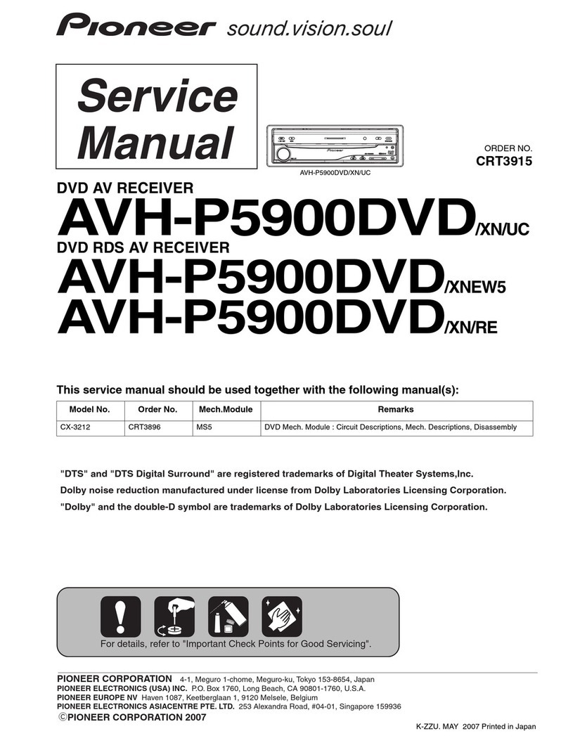
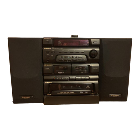
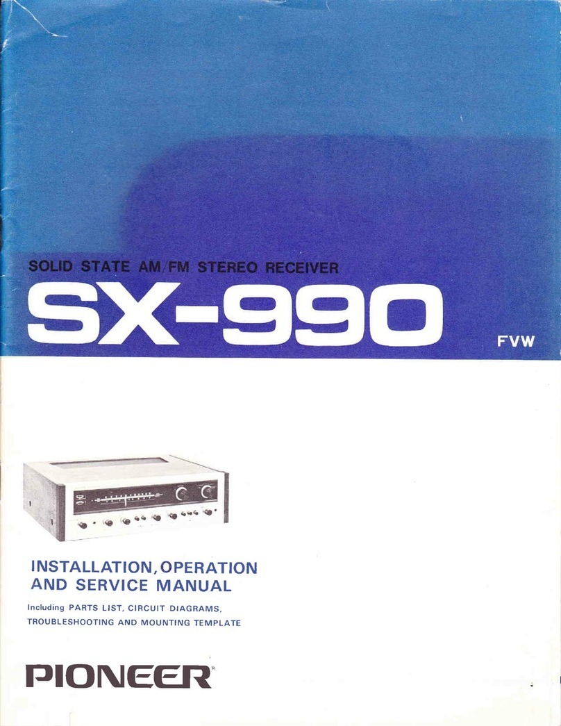
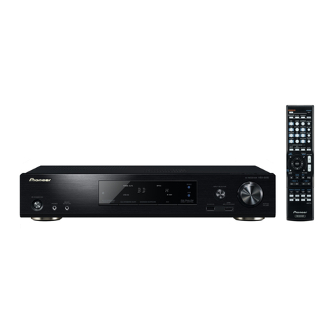
  9. Pioneer VSX-5300 User manual

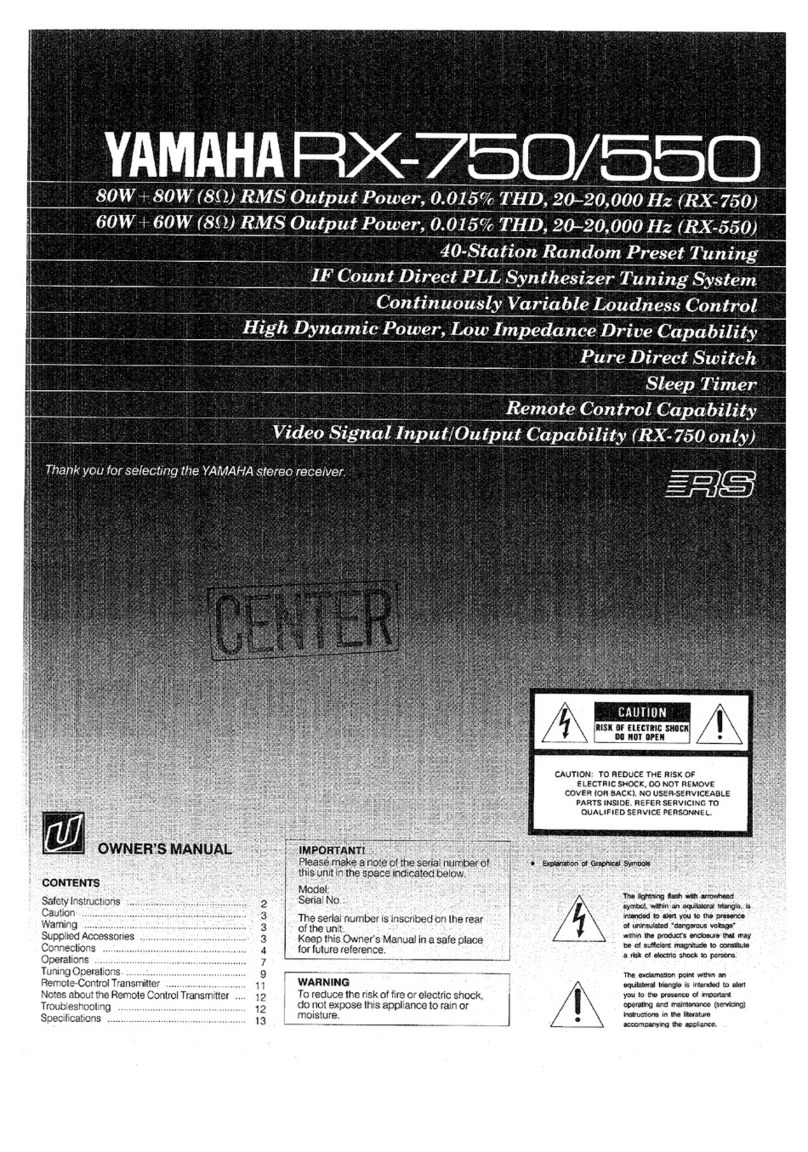
Pioneer VSX-5300 User manual

Q)
PIONEER’
The
future
of
sound
and
vision.
Service
ORDER
NO.
ARP
1597
AUDIO/VIDEO
STEREO
RECEI
VSX-5300
VSxX-5300S
VSX-5300
AND
VSX-5300S
HAVE
TWO
VERSIONS:
Applicable
Model
vsx-5300
|
VSX-5300S
|
0
|
AC120V
only
U.S.A.
and
Canada
AC110V,
120V—127V,
220V,
240V
(switchable)
Pusey
|
@
This
manual
is
applicable
to
the
VSX-5300/KUC,
SD/G
AND
VSX-5300S/KUC
types.
e
For
the
VSX-5300/SD/G
and
VSX-5300S/KUC
types,
refer
to
pages
43,
44.
©
The
“’S”
at
the
end
of
the
model
number
indicates
that
a
programable
remote
control
unit
is
supplied.
Type
Power
requirement
Export
destination
CONTENTS
1.
SAFETY
INFORMATION
.........---00585
2
2.
EXPLODED
VIEW
AND
PARTS
LIST......--
3
3.
PACKING
......
cece
eee
eee
eee
eee
6
4.
SCHEMATIC
DIAGRAM...........-50
2
eee
7
5.
P.C.
BOARDS
CONNECTION
DIAGRAM......
15
6.
ELECTRICAL
PARTS
LIST........-...54-.
31
7.
ADJUSTMENTS.
...
0...
ce
eee
ee
ee
ee
eee
37
8.
IC
DESCRIPTIONS.......-..-0
2
eee
ees
40
9.
FOR
VSX-5300/SD/G
AND
VSX-5300S/
KUC
TYPES
....
0...
cee
ee
eee
ee
ees
43
10.
PROGRAMABLE
REMOTE
CONTROL
UNIT
FOR
VSX-5300S/KUC
TYPE
(AXD1055)....--
45
11.
SPECIFICATIONS
..........2--2
22
eee
50
12.
PANEL
FACILITIES.
.........-2--20206-
51
PIONEER
ELECTRONIC
CORPORATION
=
4-1,
Meguro
1-Chome,
Meguro-ku,
Tokyo
153,
Japan
PIONEER
ELECTRONICS
SERVICE
INC.
P.O.
Box
1760,
Long
Beach,
California
90801
U.S.A.
PIONEER
ELECTRONICS
OF
CANADA,
INC.
505
Cochrane
Drive,
Markham,
Ontario
L3R 8E3
Canada
PIONEER
ELECTRONIC
[EUROPE]
N.V.
Keetberglaan
1,
2740
Beveren,
Belgium
PIONEER
ELECTRONICS
AUSTRALIA
PTY.
LTD.
178-184
Boundary
Road,
Braeside,
Victoria
3195,
Australia
TEL:
[03]
580-9911
©
PIONEER
ELECTRONIC
CORPORATION
1988
naat
MEAGRE
PRGGACUNEaR
Sx-5300
1.
SAFETY
INFORMATION
1.
SAFETY
PRECAUTIONS
The
following
check
should
be
performed
for
the
continued
protection
of
the
customer
and
service
tech-
nician.
LEAKAGE CURRENT
CHECK
Measure
leakage
current
to
a
known
earth
ground
(water
pipe,
conduit,
etc.)
by
connecting
a
leakage
current
tester
such
as
Simpson
Model
229-2
or
equivalent
between
the
earth
ground
and
all
exposed
metal
parts
of
the
appli-
ance
(input/output
terminals,
screwheads,
metal
overlays,
control
shaft,
etc.).
Plug
the
AC
line
cord
of
the
appliance
directly
into
a
120V
AC
60Hz
outlet
and
turn
the
AC
power
switch
on.
Any
current
measured
must
not
exceed
0.5mA.
A
Leakage
current
tester
Reading
should
not
be
above
0.5mA
Test
all
exposed
metal
surfaces
2-wire
cord
@
Also
test
with
}
plug
reversed
1
Earth
(Using
AC
adapter
"ground
plug
as
required)
AC
Leakage
Test
ANY
MEASUREMENTS
NOT
WITHIN
THE
LIMITS
OUTLINED
ABOVE
ARE
INDICATIVE
OF
A
PO-
TENTIAL
SHOCK
HAZARD
AND
MUST
BE
COR-
RECTED
BEFORE
RETURNING
THE
APPLIANCE
TO
THE
CUSTOMER.
2.PRODUCT
SAFETY
NOTICE
Many
electrical
and
mechanical
parts
in
the
appliance
have
special
safety
related
characteristics.
These
are
often
not
evident
from
visual
inspection
nor
the
protection
afforded
by
them
necessarily
can
be
obtained
by
using
replacement
components
rated
for
voltage,
wattage,
etc.
Replacement
parts
which
have
these
special
safety
charac-
teristics
are
identified
in
this
Service
Manual.
Electrical
components
having
such
features
are
identified
by
marking
with
a4
on
the
schematics
and
on
the
parts
list
in
this
Service
Manual.
The
use
of
a
substitute
replacement
component
which
dose
not
have
the
same
safety
characteristics
as
the
PIONEER
recommended
replacement
one,
shown
in
the
parts
list
in
this
Service
Manual,
may
create
shock,
fire,
or
other
hazards.
Product
Safety
is
continuously
under
review
and
new
instructions
are
issued
from
time
to
time.
For
the
latest
information,
always
consult-the
current
PLONEER
Service
-
Manual.
A
subscription
to,
or
additional
copies
of,
PIONEER
Service
Manual
may
be
obtained
at
a
nominal
charge
from
PIONEER.
*
NOTE
FOR
INSTALLATION
OF
VR
LED
ASSEMBLY
Step
1:
Run
the
lead
wire
(No.119)
through
the
hole
indicated
by
the
arrow
in
the
Fig.
below
from
the
face
of
panel
base
(No.28).
Front
pane!
face
VR
knob
hole
Step
2:
Run
the
lead
wire
through
the
spaces
between
the
bosses
at
the
rear
side
of
the
panel
base
as
shown
in
the
Fig.
below.
Run
one
of
the
wires
through
the
spaces
between
boss
1
and
boss
2,
and
boss
4
and
boss
5,
and
the
other
through
the
spaces
between
boss
2
and
boss
3,
and
boss
5
and
boss
6,
(Insert
the
wires
deep
between
the
bosses.)
)
ee
Oo
:
10
ye)
J
£1
(SD/G
type
only
(SD/G
type
only)
*1
Tightening
torque:
less
than
3kg°
f/cm’
*2
Tightening
torque:
less
than
5kg
+
f/cm?
AN
Ms
WY
WWE
\.
\Y
fe
<
YY
;
WY
(
‘
’
\/"
Wi
\
\\
\
2.
EXPLODED
VIEW
AND
PARTS
LIST
NOTES
:
*
Parts
without
part
number
cannot
be
supplied,
*
The
A
mark
found
on
some
component
parts
indicates
the
impotance
of
the
safety
factor
of
the
part.
Therefore,
when
replacing,
be
sure
to
use
parts
of
identical
designation,
*
Parts
marked
by
“©”
are
not
always
kept
in
stock,
Their
delivery
time
may
be
longer
than
usual
or
they
may
be
unavailable,
Parts
List
Mark
No.
oO oO
OND
oORWN—
>
bP
>
BBE
=
—_
12
>
13
>>
is
15
16
17
18
19
20
21
22
23
24
25
26
27
28
29
30
31
32
33
34
35
of
Exterior
Part
No.
AWE1076
AWZ1813
AWZ1814
AWZ1817
AWZ1818
2SA1302
28C3281
ATS1146
AKP-515
ADG1031
AKX1004
AEK-—
100
AEK
—
304
AEP—251
AAB1056
AAD1328
AAD1393
AAD1392
AAD1397
AAD1398
AKR-032
AEK—-
100
AAD
1406
AAK1514
AAK1515
AAM-—030
AMB1400
ANB1207
ANE1043
AEP
—
057
AEP
—313
ABA-—283
ABA
-—
297
Description
Tuner
assembly
AF
video
assembly
Surround
assembly
Enhancer
assembly
u
COM
display
assembly
Transistor
(Q1,
Q3)
Transistor
(Q2,
04)
Power
transformer
(T1,
AC120V)
AC
socket
3P
(AC
OUTLET)
AC
power
cord
Slide
switch
($1,
SPEAKER
IMPEDANCE)
Fuse
(FU3,
FU4,
4A//125V)
Fuse
(FU1,
8A/125V)
Knob
(MASTER
VOLUME)
Knob
(SPEAKERS
A,
B,
REAR)
Knob
(TAPE1/DAT1,
TAPE2/
DAT2
MONITOR,
CD,
PHONO)
Knob
(VCR1,
VCR2,
VDP/CDV,TUNER)
Knob
(SURROUND
OFF,
STADIUM,
S-SURROUND,
DOLBY
SURROUND)
Knob
(MUTING)
Fuse
Holder
(SD/G
type
only)
Fuse
(FU2,4A/125V,
SD/G
type
only)
Knob
(STATION
CALL)
Acrylic
panel
FL
filter
Friction
plate
Panel
base
assembly
Front
panel
Bonnet
case
Mica
sheet
Mica
sheet
Screw
Screw
M3x19
Mark
No.
36
37
38
39
40
41
42
43
44
45
46
47
48
49
50
51
52
101
102
103
104
105
106
107
108
109
110
111
112
113
114
115
116
117
118
119
120
121
122
Part
No.
ABA
-
298
ABA1006
ABA1009
ABA1011
ABA1031
ABA1052
ABE-—053
ABN
—065
VMZ30PO60FMC
BBZ26PO60FMC
FBT40PO80FZK
NK90OFUC
ABN1006
AKX1004
AKX—507
ASH—004
VMZ26P040FZK
Description
Screw
Screw
M3x8
Screw
Screw
Screw
M4x8
Screw
M3x12
Washer
Nut
Screw
Screw
Screw
Nut
Nut
Line
voltage
selector
(S2,SD/G
type
only)
(110-127/220-240V)
Line
voltage
selector
(S3,SD/G
type
only)
(110/120-127/220/240V)
Slide
switch
(S4,SD/G
type
only)
(Channel
step“FM
De
—emphasis)
Screw
(SD/G
type
only)
Power
amp
assembly
Rear
power
amp
assembly
Master
volume
assembly
SP
switch
assembly
VR
LED
assembly
Fuse
assembly
Terminal
(GND)
Chassis
Rear
panel
Panel
stay
Bottom
plate
PCB
holder
Heat
sink
holder
Heat
sink
Spacer
ring
PCB
supporter
Pin
jack
plug
Holder
Plate
(SD/G
type
only)
Lead
wire
;
PCB
supporter
PCB
supporter
Cushion
3.
PACKING
Part
List
of
Exterior
Mark
No.
akon
51
52
Part
No.
AHA1020
AHA1021
AHD1441
AEA1002
ARB1113
AXD1056
Description
Front
pad
Rear
pad
Packing
case
Antenna
set
Operating
instructions
(English)
Remote
control
unit
Packing
sheet
Battery
W4—>
Gi=tc
[ale]
oh
baat
emis
fe
arenorianctitan,
2
4.
“SCHEMATIC
DIAGRAM
(—
TUNER
ASSEMBLY
AWE1076
QTOt:
FM
RF
AMP
FM
UNBAL
1750)
FM
BAL
(3000)
AM
LooP
ANTENNA|
1.
RESISTORS
:
Indicated
in
O,
1/4W,
1,/8W,
+5%
tolerance
unless
otherwise
noted
k;kOQ,M:MQ,
(F);
41%,
(G);
£2%,
(K):
£109,
(MD;
£20%
tolerance.
2.
CAPACITORS
:
Indicated
in
capacity
(uF)
/voltage
(V)
unless
otherwise
noted
Bp:
pF.
Indication
without
voltage
is
50V
except
electrolytic
capacitor.
3.
VOLTAGE
CURRENT
:
J:
OC
vottage
(V)
at
no
input
signal.
mA:
OC
current
at
no
input
signal.
4.
OTHERS
=:
Signal
route.
@
:
Adjusting
point.
The
A
mark
found
on
some
component
parts
indicates
the
importance
of
the
safety
factor
of
the
part.
Therefore,
when
repiacing,
be
sure
w
use
paris
uf
idenial
designation.
3K
marked
capacitors
and
resistor
have
parts
numbers.
This
is
the
basic
schematic
diagram,
but
the
actual
circuit
may
vary
due
to
improvements
in
design.
Q704,Q705:
BUFFER
FM
MIXER
100
SWITCHES
(Underline
indicates
switch
position)
Outside
of
PC
board
IMPEDANCE
SELECTOR
LESS
THAN
8
-8Q
OR
MORE
S2:
VOLTAGE
SELECTOR
110-120V-220-240V
(SD/G
type
only)
$3:
VOLTAGE
SELECTOR
240/120-127/110/220V
(SD/G
type
only)
$4:
DE-EMPHASIS
75
—50pS
TUNER
ASSEMBLY
STATION
10-30
u
COM
DISPLAY
ASSEMBLY
TUNING
+
FM
TUNING
AUTO/MANUAL
REAR
LEVEL
+
BALANCE
L
TREBEL
+
BASS+
TUNING
—
AM
TUNING
DIRECT
ACCESS
R706
ww
R724
seat
ager
Q751-Q753
Q703,
Q721
Q704,
Q705
Q773:
AM
+B
ON/OFF
O773)
L733
:
STATION
CALL
+1
(SD/G
type
only)
+
MUTING
:
VCR
NOISE
FILTER
AN7470P
LA1265S
M7001
Q773,
Q775
RN2201
2SA933S
2SK161
22yH
REAR
LEVEL—
4
BALANCE
R
TREBLE
BASS—
STATION
CALL
*6!
FM
MODE
AUTO/MONO
SIMULATED
STEREO,
ACOUSTIC
MEMORY
STATION
CALL
*2
STATION
CALL
*7
MEMORY
i!
:
VIDEO
SIGNAL
SELECTOR
ACOUSTIC
SELECT
VIDEO
ENHANCER
STATION
CALL
*3
STATION
CALL
*8!
TAPE2/DAT2
eer
|
28C1740S
2SC1740SLN
2SC2668
2SC2786
EMFORCEMENT
MONAURAL
AND
EMFORCEMENT
veo
STOP
Q7o1
Q77y
D771,
0772
0731-0734,
D751
0701-0703
AM/FM
IF
DET
ae
Cea
SD.ADJ
VOLTAGE
REG
ITE
SIGNAL
pm
sg
$831
cra?
10/30
Tes
Hey
7
19KHr
£90°
|
FLIP
FLOP
3OKH?
FUP
FLOP}
2S8K241
2SK246
SVC321C2-—SP
18S252
1SV147
Q7si:
RIPPLE
FILTER
L702
$701
ASH1027
T711
ATB-O95
L771
ATB-100
T701
ATC
194
L701
ATC-1001
ATC—
1002
L705
ATC—
1003
T702
ATE-063
1732
ATE-1001
T731
ATE-
1002
R735
47%
COMPOS
‘SCH
MITT]
CIRCUIT
rT
'STEREO/MONO!
CHANGE
OVER
‘SWITCH
:
MEMORY
SCAN
$832:
$833
:
$834:
$835:
$836:
$837:
$838:
$839:
$840:
$841:
$842:
$843:
$844:
$845
:
S846:
S847:
$848:
S849:
$850:
VCRI
TAPE1/DATI
DELAY
TIME
SURROUND
OFF
STATION
CALL
*4
STATION
CALL
*9
STATION
NAME
VCR2
co
DOLBY
SURROUND
TV
ANT
VIDEO/TV
STATION
CALL
*5
STATION
CALL
*10
vOP/COV
TUNER
SURROUND
STUDIUM
POWER
STANDBY/ON
PHONO
SIMULATED
SURROUND
Ll
|
F721
ATF—107
F722
ATF-119
F751
ATF-164
F731
ATF1042
L703,
L704,
L732,
LAU2R2M
L733,
L772
L731
LAU472J
TCO771,
TC772
ACM-015
VR752
VRTB6VS224
VR751
VRTB6VS472
x771
ASS1005
X731
ATF1027
‘S6Op
SEPARATION
Q752—Q754:
MUTING
SP
SWITCH
ASSEMBLY
$380
(1/3):
SPEAKERS
A
ON-OFF
$380
(2/3);
SPEAKERS
B
ON-OFF
$380
(3/3):
SPEAKERS
REAR
ON-OFF
{p
SD/G
TYPE ONLY
Reo
ee
EE
TO
TUNER
ASSEMBLY
T5xs
$4
(FM
On
ae).
|
fo
z
+
Tae
AM
10k
Hr
1
Soys
(aM
5k
tm)
aM
9h
Hr
°
°
(ae
ee
a
©
IC
121
(4/6)
—(676),
C122
(1/5)
,
(4/5):
INPUT
SW
-—-—
139
mia?
638
Q121—
124:
BUFFER
c23
as
ary
cuz
47h
ors
crs
Jarra
ory
cia
ars
1c122(2/5),
He
(3/5):
INPUT/
OUTPUT
SW
=
"
Rt
2
101221676)
SIMULATED
|
ON
stenco
[OFF
um
ON/OFF
by
synchronizing
with
VCR
NOISE
FILTER
indicator
only
when
FUNCTION
Is
VCRI
on
VCR2.
FUNCTION
1e
No!
ci2t
(Te#164N)
1€122
(TC9164N)
1c101t
M5220P
0181
RDS
PHONO
a
5H
1c402
TC40668P
0283
ROS
cD
Sa
EL
eT
So
Ic121,
1C122
TCO164N
0276,
0404
RDS
TUNER
aE
TEEN
1c212
TC9184P
0253,
0254.9258
RDS
TAPE
/DATI
a
7
Are
1c404
»
PC7T8LOS
0285
RDG
TARER
“ATE
=
<
1C271,
1C272
u
PC78M1
2H
0289
RDB
Vert
Sa.
787
¥
5
eT
1c273
»
PC78M15H
D211,
D212
RDS
VoR2
a
sae
Q215,
Q409,
0412
=
RN1203
0251,
0252.)255-
1ss
Q410,
Q411
RN2203
0257,
D259,0277,
:
:
Q214,
315,
0401
2SA1048
D278,
0284,9290,
0291,
D293-p
296,
0319,
0401
-p
403
318
Q311,.Q312
2SA968
0287
1S1
Q271
2SB834
0271-0274
10E
Q309,
Q310
28C2238
The
jicator
only
chi
change
when
FUNCTION
ether
than VERT
or
VoRZ.
Brea
lbeNaiatS.
<secoase
Da
ae
eer.
WE
AF
Video
Assembly
Q182,
Q211,
Q212,
RY301
ASF
(C401
CX~894
Q273,
Q275, Q276,
RY271
ASF
1403
CXD1067P
Q316—Q319,
0402,
L301,
L302
ATE
1c181
CX01120P4
Q403,
0406-0408,
T271
AT
1€201,
1C213,
IC251,
MS218LF
Q471
1C252
Q413,
0414
2SC1845
C293
ACe
te2it
M5220L
Q213,
Q404,
A405
28C2878
c291
ACL
Q272,
Q274
2S8C3377
C292
ACI
6286
DSSB20F
C277,
C283
ACI
0318
HZS9AL
C289,
C290
ACI
D275
RO1S5ESB
R377,
R378
»
AC
R280
AC
1€122(2/5),
(3/5):
INPUT/
OUTPUT
SW
Qi21
—
0124:
BUFFER
XX
X
A
112216
/6)
M5220P.
TC4066BP
TC9164N
TC9184P
w
PC7BL05
uv
PC78M12H
vu
PC7T8MI5H
RN1203
RN2203
2SA1048
2SA968
2SRR34
28C2238
28C2240
28C2458
28C
1845
2S8C2878
2S8C3377
O5SB20F
HZSSAL
ROISESB
0181
0283
D276,
D404
0253,
0254,
D258
0285
0289
Dail,
0212
0251,
0252,
D255—
0257.
D259, D277,
0278,
0284, D290,
0291,
0293-0296,
0319,
D401~0403
0287
27)
~
D274
D279
-D282,
0288,
0292
Ry301
RY271
L301,
L302
Tan
C293
c29t
C292
C277,
C283
C289,
C290
RIT,
R378
R280
cre
14.7730
22x
(C
|
RDS.1ESB
ROS.1ESB1
ROS.6ESB
RDS.6ESB3
RD6.2ESB
RO8.2ESB1
RD9.1ESB
188252
ASR—112
ASR1012
ATH1004
ATTIOIS
ACG1002
ACG1005
ACHIO11
ACH1021
ACHI074
ACN-
139
ACN-209
7
—3—_—_—_—_—_—_—_—_—__
112215
/5):
SIMULATED
STEREO
ON/OFF
cai
dt
476
Priaz
47k
Ries
15k
IC
208:
SIMULATED
STEREO
[|
FRONT
LcH_L.METER
cm
of
Front
ach
meer
[|
eT
[|
FEAR
LCH
L.METER
|
(co
bd
Eee
fof
teas
sce
weren
|
peo
[ols
|
0
f_swo
[ota
Lo]
surrouno
muting
TS]
rake
fof
ees
ta
[Crsv
Tole
ie
ec
[ofr]
[of
stanzo
[[snom
[ote
|
fo]
stastea
[+sv
Tole
J
fev
[or
[_srev0sr7
+
UJ
1C251,1c2s52:
LEVEL
METER
AMP
0181,
0182:
BUFFER
Q21—
Q213:
MUTING
1c213:
CENTER
CHANNEL
iC2u,ic2i2:
ey
AMP
R2I7
a7
Q214:
BUFFER
re
cane
ee
oe
215:
MUTE
DRIVE
MASTER
VOLUME
ASSEMBLY
Master
Volume
Assembly
[sav
_|
1c241
M5220P
=e
(c24z
TA7291S
noi
|
ra
aaa}
a244
RN2201
(24)
L242
LauseoK
VR241
ACX1015
LED
ASSEMBLY
conta
IC
2412
y)
0900
I
h
mt
[fo]y
BUFFER
AMP
J
eI
VOLUME)
(“me
[ole
a2at
[vaceo
||
VOL.IND
DRIVE
i
CI
:
0990
AEL1053
Pere
errr
r
Coo
|
ICOM
DISPLAY
ASSEMBLY
AWZ
1818
1"
&
°
°
3
ERPET
EEE
TO
FRONT
POWER
AMP
IN
ole
3
b
2
3
6
P
i
i
ry
=
e
ry
2:
>
P
33
8
ra)
&
e3
FO
ft
F2
FS
sess
|
sezz
|
sezo
|
sexe
|
seas
aa
o~+
O49
0
sare
|
saz3
|
seso
|
sas7
|
seca
Bf
ft
eG
ser7
|
seza
|
ses:
|
sese
oh
oh
ee
ee
sere
|
sazs
|
se3z
|
saso
|
seas
Sat
oe oo
et
oe
se19
|
seze
|
sess
|
seao
|
seas
|
seao
Oe
St
tf
et
ff
09 OF
0
O4¢5
0-40
O40
0-40
0
sezo
|
saz7
|
sesa
|
sea:
|
sear
|
seso
9
O40
040
040
040
0400
fOk
sezt
|
seze
|
sess
|
sese
|
seas
Sieh
fh
1
Reos
jreo7 treos
breos
bRs10
Tk
=
47%
‘47k
‘47K
47k 47%
2
oa
*
=
1c801
ast
aQ801-—a8si0
0801-0812
$801~S850
L801
VR802
VR801
Vv801
x801
Remote
sensor
unit
Q801—Q810:
BUFFER
PDGO20
RN1203
2SC2458
188252
ASG-711
LAUIO1IK
ACUI029
ACU1028
AAV1055
ASS1022
AXX1005
Please
refer
to
the
enlargement
of
this
FL
display
1C451
0467,
0469
Enhancer
Assembly
M51848P
2SA1048
Q451, Q452,
Q456—
2SC2458
Q462,
0464-0466,
Q468,
0470
Q453-—Q455
0451,
D452
L451,
L457
2SC2878
28C3064
1S$S252
LAU100K
LAUIOIK
LAU180K
LAU2R2M
LAU220K
LAU270K
vy
ya]
awe
E
Ene
13
14
|
15
|
16
I
VW
"
10
I
ID
AF
VIDEO
ASSEMBLY
AWZ1813(2/3)
SURROUND
_AMP
ASSEMBLY
AWZ1814
(1/2)
IC
404:
VIDEO
FUNCTION
1401
{C403
(CXD1067P)
terminal
topic.
1172)
Pal
——
[coe
en
R542,
tk
TAPE1/DATI
R543.
tk
R544
401,0402:|.YeRE
[eensnoumy
t=}
Pes
ue
VOP/CDV
l
[sim
SURROUND
BALANCE
R514:
eat
woh
C505
Rss
R537
1
i780
si
10/50
7%
15k
339
pss
C338
i
tH
O4
sk
1750
Rsor
CSO!
By!
ho
es
vrsce:
INPUT,
OUTPUT
CONTROL,
GENEL
aos
:
CONTROLER
wae
1402172)
0403,0406:
N
BUFFER
wl
eg
pal
ouT
|
Pe
ee
VIQEO
ENHANCER
ON/OFF
R429:
10K
0404,0405:
2409,0410:
TERS
ENHANCER
MUTING
a
ON
/OFF
1C404:
1¢402(2/2)
4.7K
CxXD1120P—1
REGULATOR
1c561
LA2730
1C533
M5K4164AP
1€532
M50199P
ic501
M5201P
1C623
MS5218LF
1C562,
IC591
M5218PF
1€622
M5220P
1C531
M5233P
1C594
TC4066BP
Ia
Ttyy
tt
ott
tt
{)
=
O45
Re
caos
TO
MONITOR
TV
y
1000/10
Jd
i
6)
2
Nipeo
ha
R423
ou
)
68
0408
0413,
0414:
To
BUFFER
I
epee
2
J19
a4,
O42:
RF
MOD
ON/OFF
DEGITAL
DELAY
Q503,
Q591
RN1203
Q505, Q592,
0623
2SA1048
:
a
[1
siw0
0593,
0594
2S8C2458
a
64k
RAM
Q621,
Q622
28C2878
ia
0
D593
HZS6AL
[|
ourPuT
BUFFER
D591,
D592
RD1OESB1
D627
RDS.1ESB
D629,
D630
RDS.6ESB3
D531—D535,
0594,
188252
0621-0624,
0628,
0631
INPUT
CONTROL
1403
(CXD1067P)
terminal
logic.
(272)
rowan
|
#4]
ON
Lo
re
|
NOTE:
Parts
list
for
AF
VIDEO
ASSEMBLY
AWZ1813
{2/3)
schematic
diagram
is
included
in
the
parts
lust
for
AWZ1813(1/3)
on
pp.8-8.
anniillll
Me
ENHANCER
DELAY
TIME
NSS,
aN
tod
DoLay
1cS02:
Pa
to4
‘STADIUM
fueyate]
Ic562
(172):
ica
C591:
SURROUND
MODE
(few
T
Lsimucateo
ee)
anes
FER)
MATRIX
{Teno
TI
3
R592
R593
oie
©
TT]
47k
22.
C595
rev
Tod
EOS
10750
ioeoe
—
([y
+tay
[
[,
enmac
||
[Usrure
[oI
CJ
ENHANCER
_
ASSEMBLY
_AWZ1817
Q451,Q452
BUFFER
Q593,Q0594:
STADIUM/SIMULATED
SWITCH
|
|
Bsa
{
f
IC5S61:
¥
l
DOLBY
8B
I
0
sTanZ20
NO
SPLIT
2MHE
SPLIT
a
a
a a
a
i
0458,0459:
Q460,0461:
Wseur
od
—
—DELAY_
BUFFER
BUFFER
od
14S4
1458
L456
C460
7
foun
=
27yH
22H
Q623:
BUFFER
0623
Serene
"
Me
:
tte}
f
2ma
Dovey
LEVEL,
aan
eee
ae
oe
©)
=
&
6;
ae
am
47k
;
SYNC
SEPARATOR
g
3
By
0465,
0466
X531
BUFFER
iS
EXXSEEXE223
ERE:
‘
Q462,0464:
C473:
case
[Case
LL
sak
|
SPRIT
SCREEN
BUFFER
ae
0470:
CONTROL
O47:
RESET
START
_TRIGER
_—
°
9 3
539
e
On
c53t
O/WRITE
CONT
i
i
Tritt
tyttty
hut
BUFFER
Sle
[7
[s
RE.
ic62t
AR
an
ee
tetananaatet
ee
ee
nee,
POWER
AMP
ASSEMBLY
aie
7
Q301—
Q308,
1C301
,1C302:
Aaa
R353
POWER
AMP(1/2)
315
crm
Py
et
00
{ism
sma
R363
|
15k
D307
bers
ox0s
1
0309
ey
62.4]
zs]
Saas
NSO.
(CNSO}
Co]
+8
G
Pl
+s
|
R591
o
"e
[sis]
[oT
ease]
LoL
_EMITTER
|
0301
pe
ouT
R:
e538
a
750
ADDRESS
ENCODER
HVT
$82
113
[i419
fo
fe
Ic532
are
“ay
DEGITAL
DELAY
302
30
rh,
C308
100
Q313,
0314:
OVERLOAD
DET
.
100
I
Power
Amp
Assembly
1€301,
1C302
PAOO16
Q307,
0308
282705
—==—-6
deer
0305,
0306
-
2SA1145
®
:
cent
7{o]
am
0301,
a302
2SA979
D317
RD24ESB
wen
a
VOLUME
_&
BALANCE
btn
|
—to!
0303,
0304,
4313,
28C¢2240
0301-D316,0318,
1ss252.
nt
PREAMP
OOF
mee
‘
(ED
n
a
pe
0314 0319
REAR
POWER
AMP
L651,
L652
ATHI011
L
'
'
STORED)
|
5
!
oO
GC)
0621,0622:
SURROUND
ON/OFF
SURROUND
AMP
i
ASSEMBLY
AW2
1814
(2/2)
Q623:
BUFFER
ASR1005
Py
VR501
ACS1024
=
VR502
VRTB6EVS223
ASS1016
19
20
21
|
C)
=a
re
Lt
[|
title
©
|
“piven
39
we
Wel
C328,
ha
Q318,Q319:
Q3I7;
ASSEMBLY
AWZ1815
|
Do
DF
IC651,
IC652
»
PC1188H
=
I
AF
VIDEO
ASSEMBLY
AWZ1813
(3/3)
Q309—
0312,
Q1—
04:
n3at
{rama
POWER
AMP(2/2)
47
349
47
1
rt
rn
&
6.
RY301
Rss7r
ye
fad
.
R377
2
idite
way
:
=
sro
3391
1
R36
wordy
R389
a)
Q1,
a3
2SA1302
Q2,
A4
2S8C3281
i]
R378
lossee
RY3ON)
(i,
R297
22
9316,
0320:
RELAY
DRIVE
lz
[evo
[ols
|
[==
|]
Use
[I
U
Q273:
CURRENT
REGULATOR
SP
SWITCH
ASSEMBLY.
$380
SUL6LXXXS
s
R390
a
SPEAKERS
A
iaer
$380
‘
iz
CL
aS
|
|
PHONES
1
Eb
ro]
(mabe
(me
(mba
I
CNIS
TT
le
5
60H
Tole
UT
Tle
ee
a
7
0
$380
fat
oe
|
(34)
R
REAR
ae
bere
REAR
ag
|e]
ose
a
ve
[|
no
rao
Tecan
36]
|
9]
[REAR
SP
Ud
—_—
VIDEO
SIGNAL
ROUTE
——
—
—
ENHANCER
SIGNAL
——————_
MAIN
ROUTE
FOR
AUDIO
SIGNAL
©|-
———————_
DELAYED
SIGNAL
|
L
—
—
——
DIGITAL
SIGNAL
(BFORE
DELAY)
OR
SUB
ROUTE
FOR
AUDIO
SIGNAL
4
—
—
——
DIGITAL
SIGNAL(AFTER
DELAY)
|
©
A
O}n7
st
R
els
SPEAKERSIFRONT)
[zesvren]
in
NOTE:
Parts
list
for
AF
VIDEO
ASSEMBLY
AWZ1813
(3/3)
schematic
diagcam
is
inctuded
in
the
parts
list
for
AWZ1813(1/3)
on
pp.8-9,
td
Lo4o)
Lad
_
{C271
—1C273,Q271,Q272:
VOLTAGE
REGULATOR
[2s]
bert
be7e
J]
wen
"3!
|
FUSE_ASSEMBLY
roe
E
2
N
|_|
7
C901
ACG1005
An
Ca7T
+
POWER
TRANSFORMER
C271
me
rr
<tr
ir
C285
swt
ps)
[|
ome
a
ee
i272
R272
Le]
18(5W)
27s
rr
Or
C274
D276
me
Le
ype
esl
R283,
10
'
!
!
!
!
1
1
|
!
1
'
!
|
'
s2ovE4
1
SPEAKER
frre
IMPEOANCE
9
ov
RMC
IN
[|
[Aree
boll
[-v
rer
|
facev
[ol
pes
es
Se
ee
el
pacer
—tofs
Aint
ee
pennan
0276:
=
a274:
[ennan.c
|
|
R2s2
BUFFER
VOLTAGE
[eucx
ue
[oly
|
33K
REGULATOR
(sy
le
100
[—recay
[ois
TTT
[__cno
[le
|
of
1s
aeat
oat
[_actwey
Tots
|
284
ok
[ser
[ole
|
Ses
rut
sere
|
ol
101
TT
7
(ea)
a
t2
I
1
Pere)
Ter
lpoweR
TRANSFORMER
Al
hi
POWER,
TRNsron
fa
nen
eS
fem
x
A
a
eee
j
(ae
do93
?
AC
R
CORD
beep
——
f+}
J
:
xeaoo
Pen
10st
tov
I
5
ash
ieee
23
?
TY
Posy
t
TT
€)
Lowe
TO
d
.
|
pees
©}
(SHES)
a
Pt
x
AC
120
a
ne
Berd
(3)
6onz
oD
am
>
—€6)
!
IN
SWITCHED
RELay
Bence
“ost
uat
DRIVE
=
[ie
J
AC
OUTLETS:
{_}
AA
Ane
=
315
N
Mw
23
|
24
D
1
2
|
3
5.
P.C.
BOARDS
CONNECTION
DIAGRAM
-
External
appearance
of
transistors
and
ICs
2SA933S
28C
1740S
2SC
174
0SLN
teem
2SC
2668
ws
&)
Let
Ne
2SA968
2SB834
2SC
2238
xy
Let
No,
2SA979
28A1048
2SC
2458
28A1145
2SC
2240
28C
2705
28C
2878
2SA1302
2SC3281
2SC
2786
28C3377
Type
Ne.
15
1
2SK161
Type
No
-
i—
Let
Ne
2SK241
Type
Ne
Lot
Ne.
2S
K246
Type
No
Lot
Ne
AN7470P
CXD1120P-1
LM7001
TC9184P
CX-894
TA7291S
LA1265S
LA2730
PAOO16
TC4066BP
*
M5201P
M5218LF
M5220L
M5218PF
M5220P
M5233P
M51848P
M50199P
M5K4164AP
RN1203
RN2201
alioh
RN2203
y
TC9164N
ts
TnRenAactasang
uPC1188H
uPC78M12H
uPC78M
15H
2SC3064
lie
CXD1067P
PDG020
28C
1845
Lot
Ne
Type
No:
hve
|
4
|
e
View
from
conponent
side
NOTE
1.
This
P.C.8
connection
diagram
is
viewed
from
the
parts
mounted
side,
2.
The
parts
which
have been
mounted
on
the
board
can
be
replaced
with
those
shown
with
the
corresponding
wiring
symbols
listed
in
the
following
Table,
Corresponding
part
symbol
|
PartName
|
Transistor
Radiator
type
transistor
off.
Capacitor
(Polarity)
©
|
}
0
Capacitor
{Non-polarity)
Others
:
VR
Variable
resistor
or
Semi-fixed
resistor
3.
The
capacitor
terminal
marked
with@double
circles)
shows
negative
terminal.
4,
The
diode
terminal
marked
with
©(double
circles)
shows
cathode
side.
5,
The
transistor
terminal
to
which
E
is
affixed
shows
the
emitter.
?.C.8,
pattern
diagram
indication
S4
FOR
SO/G
TYPE
ONLY
eo
oe
DE-EMPHASIS
75yS
FM1OOkHz
)
(Since
Sous
(
FMS50kHr
AM9KHz
poccctlcntnrneee
Q753
Q7s2
Q75s1
VR752
Q754
Ic751
Q773
VR754
lc771
o774
a772
IC734
Q775
Q72t
Q704
Q705
Q703
Q702
TCT72
9701
TC7T74
STATION
(410-30)
FM
BAL
(300)
(750)
FM
UNBAL
AM
LOOP
ANTENNA
Qs09
sos
9807
9806
=
a810
802
oat
uCOM
DISPLAY
ASSEMBLY
AWZ1818
@805
=
9804
“5
geo
ago
1caot
S4
;
FOR
=
co
BATT
9
SOD/G
TYPE
3
_
ONLY
;
3
0
er
a
ee
a
,
;o
)
|
.
DE-EMPHASIS
-
as
:
75ys
f
|
fae
:
=
8
|
Caouny
$
v
|
S4555
@)
FOR
1
goes
eee
ee
a
|
Ce
|
AM9OKHz
I
|
I
Bo
Li
-
-
SURROUND
ASSEMBLY
AWZ1814
=}
>
|
ggg,
er
ES
ree
fz
v
!c621
Ic622
e594.
Q591
622
1c562
1c561
(C531
(C532
1C533
1623
g60s
—
1c501
Q503
9594
Ies91
Q621
a623
1c244
1c242
Q241
}
a, 7]
,
4
él
ar.
a
J
~a
—
i
;
9
f
:
3
(G3
»|
Ga
,
fe
<5)
—e
is
2
u
Ss
=
wes
ss
a
Y,
SS
J
®
a
'
y
iF
me
~
aad!
fc)
si
Qs
.
Bis
.
&a
i :
a
BALANCE
Jo:
‘
ee
#
STATION
[s
j
CONTROL
(10
—
30)
j
|
:
A
IN/OUT
REAR
SPEAKERS
\M
LOOP
ANTENNA
13
|
14
I
15
I
16
I
1/
j
10
I
POWER
AMP
ASSEMBLY
Q302
9304
0308
Q307
9303
0305
ic3ot
Q313
Q301
314
1c302
Q306
REAR
POWER
AMP
ASSEMBLY
(c6s52
1c654
“0
ng
ooo0000
SP
SWITCH
ASSEMBLY
SPEAKERS
PHONES
A
B
REAR
Q310
Q3i2
Q317
,
ic252.
318
a3ait
PROTECTIO
wee
ae
Q319
a316
Q309
fo
9
0B,0,0J0..
18
Q320
R
OQ
For_OE
&
iO
a3
BE
tata
to
f
b
a
;
®
we
s,
*
Sf
we
1c251
;
by
an
ASN
ms
&
bE
0
»
a
—
om
2
6)
i
#
me
CENYR.
gee
habla
Pm
. :
oe
anes
mk
il
Pad
:
1c213
Q215
{r+
oF
RY301
1c273
aN
(C272
=
ic18i
z
Ww
(¢)
tc2u
1c2i2
Q273
©)
aai2
ae
e2it
271
Bu
9213
ew
i)
q1e2
<e)
Or
Q272
wz:
co
aU
ai25
1201
a124
1c403
at26
ai23
aao1
e402
9276
a122
©
a
1c404
2409
Q403
{
1evg
ici2t
:
0404
(122g
gos
ic4o2
0406
oa7a
Q407
Q413
9408
414
1c404
eat
Q275
Q4i2
13
TO
RF
MODULATOR
SPEAKERS
(
FRONT)
PHONE
cp
REC
PLAY
REC
PLAY
PRE
AMP
POWEP
vpP
out
'N
OUT:
IN
TO
MONITOR
ouT
AMP
IN
/CDV
vcRt
VCR2
Tv
VIDEO
OUT
>?
SWITCH
ASSEMBLY
SPEAKERS
REAR
nine
cael
|
|
ee
TH
POWER
TRANSFORMER
OF
Oo
On
Ww2z2Z
Wenw
>w«
sud
Oo
zs
gaa
<
ew
ones
SEEN
Aah
HOD
tu
cS
es
Sousa
&
inion
«
i
rort
DOO,
Og
VME
OVS
RS
Le
anes
Dn
an
OF
2zo
ad
-
ZS
<uwe
zB
it
Pe
O—-NOEO
GL
st
EOF
=
Cole)
[ES
“ort
OF
Sa
Zz
LD”
pine
26
Fries
mb
Ww
oO
Obgelnerree
>
Ww
=O
ne
Ue
ac
tee)
feame
iPr
nou
er
ne
Nag
Ode)
10
[amin
st
IMPEDANCE
SELECTOR
LESS
ea
THAN
——-
OR
Ba
MORE
AC120V
60Hz
SWITCHED
UNSWITCHED
300W
MAX
100W
MAX
fe
ae
OUTLETS
eee
|
ENHANCER
ASSEMBLY
AWZ1817
e468
1c4s1
Q47i
Q470
0469:
0482
|
0483
|
0455
|
0454!
467
'
Q458:
0451)
0456
Q466
0462:
Q464.
Q465
Q459
Q460
Qa6r-
Q457
FOR
SO/G
TYPE
TO
AF
VIDEO
ASSEMBLY
J24
A
p
1
:
me
18]
|
AES
ome
AF
VIDEO
ASSEMBLY
a
REPLACER
‘SHOU
THE
SAME.
HG
ONLY
.
HAZARD,
REPU
BCEMENT
FUSES
TION
-POUR
ENTETR
FS
MEME
YPES
ET
UNI
QUEMENT
VOLTAGE
SELECTOR
240/4120-127V/110/220V
AC
POWER
CORD
AC
110/120-1127
1220/240V
50/60Hz
SWITCHED
UNSWITCHED
300W
MAX
400W
MAX
Uo
seaaege
OUTLETS
ee
24
24
A>
Ciatciel
oe
ial
23
AS
39YT
d\0de
HOF
OT
O30IV
AA
YIGMa22A
PSL
{
i
'T
Q
A
nawos
/}\
sua
AAMAOAHAAT
>
:
O3QIvV
3A
YJGMa2eA
eine
as
u
Otkw
>
>
ok
2
1
=.
Ww
WwW
DUIS
Verge
an:
W
CoS
saecos
Bragge
Cc:
KMS
q
*
ce
yc
OF
E98
<ivo
sue
oF
Eo
AOTIZIjIZ2
JOATIOV
VOSSNONAVTS!-OSINORS
TSt-OSI\Ot
OA
VOPS\OSS\
xsHO@\0E
Q3HOTIW2NU
G3HOTIWe
XAM
WOOE
XAM
WOOt
A
ee
sek
@T3ITUO
OA
ame
8ahD
teas
tTao
oveo
eaao
Stao
Esa
aaso
EST)
Taao
Beh0
teao
dead
83R0
Sano
$380
zaao
ecao
0aa0
tango
Toad
i)
I
e
View
from
soldering
side
VIStSWA
YJIEGM3e@e@A
AZQVAHUS
Va
I
YIGM3eeA
3eus
YJIGM322A
HOTIWe
S
2ABnARIe
tT
AIWwWOF
AAMAOIOMART
‘TEe
BITES
wets
qnuuL
4
ss
Woe
Y
206°
SA.
bed
=
C
ai
ial
oe
aa
=
9
Se
Sue
Bowel
ig]
ue
ones
Te
Te
Sas
eat
Susy
OSS
Suro,
Ow
~<|
G6
SO.r
ky
s20g
7
suds.
eae.
CO2>
xp
5
LO
nr
OD
a
.:
eae
m4
ef
Zh:
Lo):
x}.
Hod
2
Q
aonAg3aMI
iE
AOTIFZIFe
i€
qs
as
hog
Be
er
Q3KITIWenU
Q3HOTIWe
XAM
WOOF
XAM
WOOE
een
es
eae
rs
YIGM32@2A
GMA
ARBWOS
80E0
AOED
SOEO
EOEO
=TOEO
a0ED
SOED
PtEO toEO
ErEO
10E91
20E0
YIGM322A
GMA
ASWOF
AARF
raaar
S290!
ia
piaaaolawuman
cies
ne
Lx
Of
i
amg
tee
i
YJGM3eeA
HOTIWe
Ge
2A3NAR9I2e
SVE)
OOF
nouns
‘emmy,
=
=
us
is
ae
ape
g
Yap”
praGaananaing
(57h
sulzoltoo
ot
=
oe:
SEES)
or
Se
Pal
gl
fe
coacenneo
@
:
220
8
Bade
ou
Bins
GO]
O”
Oreo
SIEO
THEO
theo
@rzeO
=
sasor
eoto
areo
ere
osto
BIEO
reso
)
atso
Ersor
ETSOI
3
=
‘
svsol
aaa
s
arso
5
tarot
n
stsoi
ttsot
=
ao
So:
=
SEES
ETSso
ws
Ow
rs)
Ine
(0)
—
:
0G
stso
ive
vs
ttso
A
Erso
ce
Lu
sto
:
stso
pee
asto
ee
rosor
*,
(IMA.
BO)
=}
E0B91
aStO
,2:|
|/0258;0)
Oe
or
ota,
astro
of
9
F-
Gog
FE
too
Esto
ead
¢
i
atso
SOR
ssto
tsto
topol
‘eono
E080
a
'
He
tstor
ior!
5:
ia
BORO
:
i:
soao!
2oap
S89!
ae
atso
Boke
TORO
BOBO
Erao
POPS!
AMO
treo
avso
StaO
aA
OT
(THOAA)
SAaWHARIS
AOTAJUGOM
ROTINOM
OT
MA
3Rq
YAIF
o3n
YAIT
O38
ao
3MOHS
VT
SAOV
VaoN\
Wt
IMA
“Tuo
Tuo
o3dIv)™
|
Bt
|
vr
|
at
|
ar
|
ft
|
Et
st
|
it
|
Or
|
e
|
8
|
t
e
View
from
soldering
side
f
soso
e080
180
-
$080
oreo 8080
=:
YOO
tosal
roso
=:
E080
D
080
=
2080
BIStSWA
YJEGMseeA
YAIGe!Id
MODW
toBAV
SOB8AV
9
P
dor
{for/
fon
FH
BE
Pal-ae
lo
lo
lelo
f
j
A
AAA
WW
Bo
fo
fo.
fo
fo
fo”)
Oo
z
oF
YJamMaeed
34
7
m
la
iv
or
PIBISWA
YIGM3eeA
QNUOARVe
sezo
EE291
sé2o1
1291
razol
sazol
ssa0rezo
pezol
ssao1
1sa9l
aM
aah
aean
Esao
-tSaO
reed!
peso
E080
roast
aoap
=
&
89!
OM.
Bue
Tpss32-30
iS
Ma
e
|
tRSOI
S908"
maa
Sasol
teso
jmn|etogin
8
Ben”
asp
a
|
7
ad
i
ae
oolgg0
Ja
3xAM
AST
HS
BJOMVAJAS
AOATHOS
TUONMI
2@A3SNARIS
AAZA
be
ROA
349YT
o\de
Y1INO
a
ce
im
|
212AHIM3—30
euet
(
oir
SHAOtMA
eyoe
sHAOaMa
)
sHHOMA
bs
Se
ee
eee
ce
MOITATS
(o&—Ot)
F005
MA
AWASTHA
he
AOR
39YT
o\de
YINO
Ezto
beTO
servo
tevor
EYTO
tvTO
tTTO
stvTo
rsv¥O
evTO
e0vTO
AaOTO
E0va
tETOr
sovo
tovo
OYOrAWA
Y.IGM3eeA
ASMWUT
)
)
SHACMA
eyet
sHAOOIMA
SHAOMMA
2yoe
sH¥O@M3
212AHIM3—30
(
>
a
e
2
SYVOT
Po
ead
pe
9
wae
BPPB
6°28
%
Bee
ak
A
St
9
oO
ong
Ls
ad
JAgKU
MA
(Ney)
Food
MA
ANKZTHA
WOITAT2
(O&—Or)
30
VvSsSxX-5300
6.
ELECTRICAL
PARTS
LIST
NOTES
:
¢
Parts
without
part
number
cannot
be
supplied,
*
Parts
marked
by
“©”
are
not
always
kept
in
stock.
Their
delivery
time
may
be
longer
than
usual
or
they
may
be
unavailat
*
The
A
mark
found
on
some
component
parts
indicates
the
impotance
of
the
safety
factor
of
the
part.
Therefore,
wh
replacing,
be
sure
to
use
parts
of
identical
designation.
«
When
ordering
resistors,
first
convert
resistance
values
into
code
form
as
shown
in
the
following
examples,
Ex.1
When
there
are
2
effective
digits
(any
digit
apart
from
0),
such
as
560
ohm
and
47k
ohm
(tolerance
is
shown
J=5%,
and
K=10%).
Part
No.
28017408
2SC1740SLN
2SC2668
28C2786
2SK161
2S8K241
2SK246
a
$VC321C2-SP,
18S252
18V147
Part
No.
ASH1027
Part
No.
ATB-095
ATB-100
ATC~194
ATC~
1001
ATC-
1002
ATC~
1003
ATE-063
ATE-1001
ATE-
1002
ATF-107
ATF-119
ATF~-164
ATF1042
LAU2R2M
LTA472J
5602
56X10!
561
RD1/4PS
[5]
[6]
[1]
J
47kQ
47X10?
473
RD1/4PS
[4]{7]]
J
0.52
ORG
rreerecceccesesscnseesccersenceacseceneeaes
---RN2H
[O}R][5]
K
1Q
OO
rerceesseescccereeesssseseeecceeeeseesessessersueensseesenesasseeeeeeeenaneseseneneeeeeaes
RSIP
{0}
(i)
[0]
K
Ex.2
When
there
are
3
effective
digits
(such
as
in
high
precision
metal
film
resistors),
B.G2k
GQ
BEZX1O!
—_
GDL
eveeeevessssesscceeeeseeesssssereeesnssecennnsacsesensonsseverseaearees
RN1/4SR
(ey(6l[2]G)
F
Miscellaneous
Parts
Mark
Symbol
&
Description
P,
C.
BOARD
ASSEMBLIES
Q751-0753
Q772
Mark
Symbol
&
Description
Part
No.
Q703,
Q721
Q702
Tuner
assembly
AWE1076
Q704,
Q705
AF
video
assembly
AWZ1813
Surround
assembly
AWZ1814
Q701
Enhancer
assembly
AWZ1817
Q771
u
COM
display
assembly
AWZ1818
D771,
0772
D731-D734,
D751
Power
amp
assembly
D701
—D703
Rear
amp
assembly
Master
volume
assembly
SWITCHES
-.
.-.
SP
switch
assembly
:
a
:
VR
LED
assembly
Mark
Symbol
&
Description
Fuse
assembly
$701
Slide
switch
(STATION)
OTHERS
COILS,
TRANSFORMERS
AND
FILTERS
Mark
Symbo!_
&
Description
Part
No.
Mark
Symbol
&
Description
4
Q1,
Q3
2SA1302
T7771
AM
ANT
transformer
A
Q2,
A4
2803281
L771
AM
OSC
coil
AN
Ti
Power
transformer
(AC120V)
ATS1146
_T701
FM
RF
transformer
ay
AC
socket
3P
(AC
OUTLET)
AKP-515
L701
FM
coil
a
FU3,
FU4
Fuse
(4A/125V)
AEK-100
L702
FM
coil
an
FU1
Fuse
(8A/125V)
AEK
—304
L705
FM
coil
A
AC
power
cord
ADG1031
T702
FM
Matching
transformer
cf,
$1
Slide
switch
AKX1004
T732
FM
detection
transformer
(SPEAKER
IMPEDANCE)
T731
FM
detection
transformer
Remote
contro!
unit
AX0D1056
F721
FM
ceramic
filter
Tuner
Assembly
(AWE1076)
F722
FM
ceramic
filter
F751
Low-—pass
filter
SEMICONDUCTORS
F731
AM
ceramic
filter
L703,
L704,
L732,
L733,
L772
Mark
Symbol
&
Description
Part
No.
Inductor
L731
Inductor
1C751
AN7470P
1C731
LA1265S
1C771
LM7001
Q773,
Q775
RN2201
Q754
2SA933S
31
CAPACITORS
Mark
Symbol
&
Description
TC771,
TC772
Ceramic
trimmer
C764
C708
C706
C774
C713,
C779,
C781,
C782
C714
C701,
C704,
C705
C702
C744
C745
C716
C715
C709
C752
C757
C778
C742
C743
C756
C731,
C737,
C776
C751
C738
C734,
C755
C784,
C785
C733,
C761,
C762
C723,
C758,
C763
_
C736
C721,
C722,
C771
C780,
C786
C735
-C773,
C777,
C717,
C732,
C739,
C740,
C765,
C753
C703,
€710-C712,
C719,
C720
C741
C783
C759,
C760
C766,
C767
C775
C754
RESISTORS
Mark
Symbol
&
Description
VR752
Semi-—fixed
VR751
Semi-fixed
(VCO
ADJ)
Other
resistors
OTHERS
Mark
Symbol
&
Description
32
X771
Crystal
resonator
X731
Ceramic
resonator
Terminal
4P
CANT)
Part
No.
ACM-015
CCCSL121J50
CCDCHO10C50
CCDCHO20C50
CCDCHO70D50
CCDCH150J50
CCDCH330J50
CCDRH330J550
CCDRH390J50
CCDSL221J50
CCDSL470J50
CCDTH180J50
CCMCHO80D50
CCMSL101J50
CEANP3R3M50
CEASR22M50
CEASR47M50
CEASOR1M50
CEASO10M50
CEAS1R5M50
CEAS100MSO
CEAS101M16
CEAS2R2M50
CEAS3R3M50
CEAS330M16
CEAS4R7M50
CEAS470M16
CFTXA683J50
~
CGMYX103M16
CKCYB472K50
CKCYX473M25
CKDYF103Z50
CKDYF223Z50
CKDYX473M25
CQMA102J50
CQMAS561J50
CQSA431J50
CQSA471J50
Part
No,
VRTB6VS224
VRTB6VS472
RD’%PMOOOJ
Part
No.
ASS1005
ATF1027
AKA1003
AF
Video
Assembly
(AWZ1813)
SEMICONDUCTORS
Mark
Symbol
&
Description
Part
No.
1C401
CX-894
1C403
CXD1067P
10181
CXD1120P-1
1C201, 1C213,
1C251,
1C252
M5218LF
{C211
M5220L
1C101
M5220P
{C402
TC4066BP
1C121,
IC122
TC9164N
{C212
TC9184P
1C404
yu
PC78L05
IC271,
IC272
u
PC78M12H
1C273
u
PC78M15H
Q215,
0409,
0412
RN1203
Q410,
Q411
RN2203
Q214,
Q315,
0401
2SA1048
Q311,
Q312
2SA968
Q271
2SB834
Q309,
0310
2SC2238
Q320
2802240
Q121-Q126,
Q181,
Q182,
Q211,2SC2458
Q212,
Q273,
0275,
0276,
Q316-—Q319,
Q402,
2403,
Q406-0408,
Q471
Q413,
0414
2801845
Q213,
0404,
Q405
2802878
Q272,
Q274
2S8C3377
D286
DSSB20F
D318
HZS9AL
D275
RD15ESB
D181
RD5.1ESB
D283
RD5.1ESB1
D276,
D404
RD5.6ESB
D253,
D254,
D258
RD5.6ESB3
D285
RD6.2ESB
D289
RD8.2ESB1
0211,
D212
RD9.1ESB
D251, D252,
D255-D257,
D259,
1SS252
D277,
D278,
0284, D290, D291,
D293-—D296,
D319,
D401-D403
D287
1$1555
D271
-D274
{OE2FD
D279-D282,
0288,
D292
11E2
RELAYS
Mark
Symbol
&
Description
Part
No.
RY301
Relay
(PROTECTION)
ASR-112
RY271
Relay
(POWER)
ASR1012
COILS
AND
TRANSFORMERS
Symbol
&
Description
Part
No.
L301,
L302
AF
choke
coil
ATH1004
T271
Power
transformer
ATT1015
(AC120V)
CAPACITORS
Mark
Symbol
&
Description
C293
(0.01
»
F“AC400V)
C291
(0.01
»
F/AC150V)
C292
(47
u
F/5.5V)
C277,
C283
(4300
n
F/35V)
C289,
C280
(8200
nu
F/71V)
C317-C320
C101,
C102
C121,
C122,
C125—-C134
C407
C216,
C217
C103,
C104
C285
C251
-C253
C139,
C140,
C214,
C215,
C148,
C284,
C411
C226,
C227,
C201
C181
C329
C113,
C114
C282:
C406
C116
C111,
C112
C281
C409
C272
C273
C123,
C124,
C141-C144,
C146,
C147,
C182-C185,
C202, C213,
C228,
C230,
C410
C274
C211,
C212,
C271, C278,
C279,
C286,
C287,
C401—C403,
C408
C275,
C280
C284
C288
C105,
C106,
C328,
C404,
C405
C276
C323
-C326
C137,
C138,
C220,
C221,
C224,
C225
C107,
C108
C204
C203
C109,
C110,
C218,
C219
C115
C327
C231,
C232
C222,
C223
C135,
C136
RESISTORS
Mark
Symbol
&
Description
33
R377,
R378
(0.33
2,
SWx2)
R280
(2.2M2,
“%W)
R341
—-R344
R359,
R360,
R365,
R366
R271
Part
No.
ACG1002
ACG1005
ACH1011
ACH1021
ACH1074
CCCSL101K500
CCCSL221J50
CCMSL101J50
CCMSL330J50
CCMSL680J50
CEANL100M16
CEANP3R3M50
CEASR47M50
CEASO10M50
CEAS100M25
CEAS100M50
CEAS101M16
CEAS101M25
CEAS101M35
CEAS102M10
CEHAQ010M50
CEAS2R2M50
CEAS220M16
CEAS220M50
CEAS221M35
CEHAQ470M16
CEAS4R7M50°
©
CEHAQ010M50
CEAS470M16
CEAS470M25
CEAS470M50
CEAS471M25
CEAS471M6
CEHAQ101M35
CFTXA104J50
CFTXA153J50
CFTXA243J50
CQMA332J50
CFTXA333J50°
CFTXA823J50
CKCYX473M25
CKDYX473M25
CQMA222J50
CQMA272J50
CQMA682J50
Part
No.
ACN-
139
ACN-209
RFAY%PS4R7J
RS1LMF100J
RS3LMF330J
Mark
Symbol
&
Description
Part
No.
R288,
R272
RTS5PHOOIOK
R117,
R118,
R273,
R276,
R277,
ROYPMFOOO
R283, R284,
R289,
R297,
R337
—R340,
R349-R352,
R370
R296,
R414,
R415,
R421
ROYPMOOOs
Other
resistors
RDY%PMOOO
OTHERS
Mark
Symbol
&
Description
Part
No.
Pin
jack
4P
AKB1007
Pin
jack
6P
AKB1008
Pin
jack
3P
AKB1021
Pin
jack
4P
AKB1033
Pin
jack
2P
AKB1060
Pin
jack
3P
:
AKB1061
Terminal
8P
(FRONT
SPEAKERS)
AKE-111
DIN
socket
5P
(VIDEO
OUT)
AKP-081
Screw
ABA1012
Surround
Assembly
(AWZ1814)
SEMICONDUCTORS
Mark
Symbo!_
&
Description
Part
No.
IC621
CXD1120P—-
1%
IC561
LA2730
¢
IC533
M5K4164AP
IC532
M50199P
10501
»
M5201P
Ic623
*
MB218LF
C562,
IC591
M5218PF
IC622
M5220P
IC531
M5233P
C594
TCAO66BP
Q503,
0591
RN
1203
Q505,
Q592,
Q623
258A
1048
Q593,
Q594
2802458
Q621,
Q622
28C2878
D593
HZS6AL
D591,
D592
RD
10ESB1
D627
RDS.1ESB
D629,
D630
RD5.6ESB3
D531-—D535,
D594,
D621
-
D624,
1$S252
D628,
D631
RELAYS
Mark
Symbol
&
Description
Part
No.
RY501
Relay
AS
R1005
(REAR
SP
ON/OFF)
COILS
Mark
Symbol
&
Description
Part
No.
L531
Inductor
LA.
U2R2M
CAPACITORS
Mark
Symbol
_&
Description
C565
C538
C542
C571
C628,
C629
CS01,
C502,
C505,
C553,
C561,
C562,
C564,
C566,
C567,
C574,
C591
C531,
C568,
C594,
C595,
C621
-—C625
C534,
C549,
C576
C503,
C504
C575,
C631
C633,
C634
C548, C592,
C593
C545
C544
C539,
C543,
C572
C635,
C636
C570,
C573
C551,
C552
C533,
C550
C630
C563
C577,
C637,
C638
C532,
C536,
C540
C569
C537,
C541
RESISTORS
Mark
Symbol
&
Description
VR501
Variable
resistor
VR502
Semi-—fixed
R619
Other
resistors
OTHERS
Mark
Symbol
&
Description
X531
Ceramic
resonator
Terminal
4P
(REAR
SPEAKERS)
Mini
jack
2P
(CONTROL
IN/OUT)
Part
No.
CCMSL470J50
CEANPO10M50
CEANP4R7M35
CEASR33M50
CEASR47M50
CEASO10M50
CEAS100M50
CEAS101M10
CEAS101M25
CEAS220M16
CEAS221M10
CEAS470M10
CEAS470M16
CFTXA103J50
CFTXA104J550
CFTXA123J50
CFTXA333J50
CFTXA823J50
CGMYX103M16
CKCYX103M25
CKMYB471K50
CQMA472J350
CQMA562JN50
CQMA682J50
CQSA561J50
___
Part
No.
ACS1024
VRTB6VS223
RD%PMF
OOO
J
RD%PMOODYJ
Part
No.
ASS1016
AKE1012
AKN1006
Enhancer
Assembly
(AWZ1817)
SEMICONDUCTORS
Mark
Symbol
&
Description
34
IC
451
Q467,
0469
Q451,
0452,
0456-0462,
0464-0466,
0468,
0470
Q463
Q453-
0455
D451,
0452
Part
No.
M51848P
2SA1048
28C2458
2802878
2803064
1$$252
COILS
Mark
Symbol
&
Description
Part
No,
L454
LAU100K
L451,
L457
LAUTO1K
L453
LAU180K
L452
LAU2R2M
L456
LAU220K
L455
LAU270K
CAPACITORS
Mark
Symbo!
&
Description
Part
No.
C453
CCCCH101J50
C475
CCDSL151J50
C451
CCMCH180J50
C457-C459,
C467
CCMCH220J50
C454
CCMSLO80D50
C468
CCMSL101J50
C465
CCMSL470J50
C472
CCMSL680J50
C456
CEAS100M25
C462,
C464
CEAS100M50
C460,
C461,
C463,
C471,
C473,
CEAS470M16
C474
C466
CFTXA104J50
C455
CGMYX103M16
C469
CKCYX103M25
C452
CQSA102J50
C470
CQSA681J50
RESISTORS
Mark
Symbol
&
Description
Part
No.
All
resistors
RD%PMOIDIOJ
OTHERS
Mark
Symbol
&
Description
Part
No.
Socket
OP
AKP—046
u
COM
Display
Assembly
(AWZ1818)
SEMICONDUCTORS
Mark
Symbol
&
Description
IC801
Q811
Q801-0810
D801
—-D812
Part
No.
PDGO20
RN1203
28C2458
1$$252

Other manuals for VSX-5300

1

This manual suits for next models

1

Other Pioneer Stereo Receiver manuals

Pioneer DMH-ZS9350BT Use and care manual

Pioneer

Pioneer DMH-ZS9350BT Use and care manual

Pioneer QX-9900 User manual

Pioneer

Pioneer QX-9900 User manual

Pioneer VSX-454 User manual

Pioneer

Pioneer VSX-454 User manual

Pioneer VSX-416-K User manual

Pioneer

Pioneer VSX-416-K User manual

Pioneer SX-50 User manual

Pioneer

Pioneer SX-50 User manual

Pioneer AVH-A2350BT User manual

Pioneer

Pioneer AVH-A2350BT User manual

Pioneer Elite VSX-LX104 User manual

Pioneer

Pioneer Elite VSX-LX104 User manual

Pioneer VSX-834 Manual

Pioneer

Pioneer VSX-834 Manual

Pioneer SX-1500T User manual

Pioneer

Pioneer SX-1500T User manual

Pioneer VSX-534 User manual

Pioneer

Pioneer VSX-534 User manual

Pioneer VSX-5400 User manual

Pioneer

Pioneer VSX-5400 User manual

Pioneer VSX-532 User manual

Pioneer

Pioneer VSX-532 User manual

Pioneer Siriusxm DMH-2660NEX User manual

Pioneer

Pioneer Siriusxm DMH-2660NEX User manual

Pioneer XR-VS500D User manual

Pioneer

Pioneer XR-VS500D User manual

Pioneer ELITE VSX-LX505 Manual

Pioneer

Pioneer ELITE VSX-LX505 Manual

Pioneer SPH-EVO62DAB User manual

Pioneer

Pioneer SPH-EVO62DAB User manual

Pioneer SX-939 User manual

Pioneer

Pioneer SX-939 User manual

Pioneer SX-450 User manual

Pioneer

Pioneer SX-450 User manual

Pioneer SX-202 User manual

Pioneer

Pioneer SX-202 User manual

Pioneer VSX-D466S User manual

Pioneer

Pioneer VSX-D466S User manual

Pioneer XRB3059-A User manual

Pioneer

Pioneer XRB3059-A User manual

Pioneer SX-40 User manual

Pioneer

Pioneer SX-40 User manual

Pioneer XR-VS400 User manual

Pioneer

Pioneer XR-VS400 User manual

Pioneer VSX-322-K User manual

Pioneer

Pioneer VSX-322-K User manual

Popular Stereo Receiver manuals by other brands
Sony HCD-GP7 Service manual

Sony

Sony HCD-GP7 Service manual

Sherwood RX-773 operating instructions

Sherwood

Sherwood RX-773 operating instructions

Kenwood KRF-V7771D Setup

Kenwood

Kenwood KRF-V7771D Setup

Marantz NR1710 quick start guide

Marantz

Marantz NR1710 quick start guide

Kenwood KR-V888D instruction manual

Kenwood

Kenwood KR-V888D instruction manual

Sony STR-K790 - Lifier Service manual

Sony

Sony STR-K790 - Lifier Service manual

Sangean PR-D5CL brochure

Sangean

Sangean PR-D5CL brochure

Denon AVR-1907 operating instructions

Denon

Denon AVR-1907 operating instructions

AEG SR 4360 BT instruction manual

AEG

AEG SR 4360 BT instruction manual

Kenwood KR-A5520 instruction manual

Kenwood

Kenwood KR-A5520 instruction manual

Philips FR-963 user manual

Philips

Philips FR-963 user manual

Sony XAV-AX3250 operating instructions

Sony

Sony XAV-AX3250 operating instructions

Sony STR-DE998 - A/v Receiver Specifications

Sony

Sony STR-DE998 - A/v Receiver Specifications

Kenwood KR-770 instruction manual

Kenwood

Kenwood KR-770 instruction manual

Cambridge Audio Evo 150 user manual

Cambridge Audio

Cambridge Audio Evo 150 user manual

Yamaha RX-V1070 Service manual

Yamaha

Yamaha RX-V1070 Service manual

Sony STR-DE885 operating instructions

Sony

Sony STR-DE885 operating instructions

Magnadyne LS3500CDB owner's manual

Magnadyne

Magnadyne LS3500CDB owner's manual

manuals.online logo
manuals.online logoBrands
  • About & Mission
  • Contact us
  • Privacy Policy
  • Terms and Conditions

Copyright 2025 Manuals.Online. All Rights Reserved.