PLX Technology PEX 8624-AA RDK Quick user guide

PEX 8624-AA RDK
Hardware Reference Manual
Version 1.1
May 2010
Website: www.plxtech.com
Technical Support: www.plxtech.com/support
Copyright © 2010 by PLX Technology, Inc. All Rights Reserved – Version 1.1
May 03, 2010

© 2010 PLX Technology, Inc. All rights reserved.
PLX Technology, Inc. retains the right to make changes to this product at any time, without notice. Products may have minor
variations to this publication, known as errata. PLX assumes no liability whatsoever, including infringement of any patent or
copyright, for sale and use of PLX products.
PLX Technology and the PLX logo are registered trademarks of PLX Technology, Inc.
Other brands and names are the property of their respective owners.
Document Number: PEX8624-AA-RDK-HRM-1.1
May 3, 2010

PEX 8624-AA RDK Hardware Reference Manual – Version 1.1
Copyright © 2010 by PLX Technology, Inc. All rights reserved i
PREFACE
NOTICE
This document contains PLX Confidential and Proprietary information. The contents of this document may not be
copied nor duplicated in any form, in whole or in part, without prior written consent from PLX Technology, Inc.
PLX provides the information and data included in this document for your benefit, but it is not possible to entirely
verify and test all the information, in all circumstances, particularly information relating to non-PLX manufactured
products. PLX makes neither warranty nor representation relating to the quality, content, or adequacy of this
information. The information in this document is subject to change without notice. Although every effort has been
made to ensure the accuracy of this manual, PLX shall not be liable for any errors, incidental, or consequential
damages in connection with the furnishing, performance, or use of this manual or examples herein. PLX assumes
no responsibility for damage or loss resulting from the use of this manual, for loss or claims by third parties, which
may arise through the use of the RDK, or for any damage or loss caused by deletion of data as a result of
malfunction or repair.
ABOUT THIS MANUAL
This document describes the PLX PEX 8624-AA RDK, a Rapid Development Kit, from a hardware perspective. It
contains a description of all major functional circuit blocks on the board and also is a reference for the creation of
software for this product. This manual also includes complete schematics and bill of materials.
Note: This Hardware Reference Manual is specific to the PEX 8624 RDK. In the event of a discrepancy
between this Hardware Reference Manual and the PEX 8624 Data Book, please be sure to follow the
instructions and guidelines as stated in the PEX 8624 Data Book when designing your systems.
REVISION HISTORY
Date Version Comments
1/2/2008 0.81 Hardware Reference Manual initial release.
1/18/2008 0.82 Added SHP configuration, updated the BOM and schematics.
2/8/2008 0.83 Updated Table 2-4 and schematics.
4/11/2008 1.0 Updated BOM and Schematics.
5/3/2010 1.1
Updated BOM and Schematics for the replacement On Semi CAT25080LI-G
EEPROM. Added note to follower Data Book in the case of a discrepancy
with Hardware Reference Manual in “About This Manual” section.

PEX 8624-AA RDK Hardware Reference Manual – Version 1.1
Copyright © 2010 by PLX Technology, Inc. All rights reserved ii
CONTENTS
NOTICE ......................................................................................................................................................... i
ABOUT THIS MANUAL .................................................................................................................................. i
REVISION HISTORY ...................................................................................................................................i
1.General Information.............................................................................................................................1
1.1PEX 8624 Features....................................................................................................................... 2
1.2PEX 8624-AA RDK Features...................................................................................................... 3
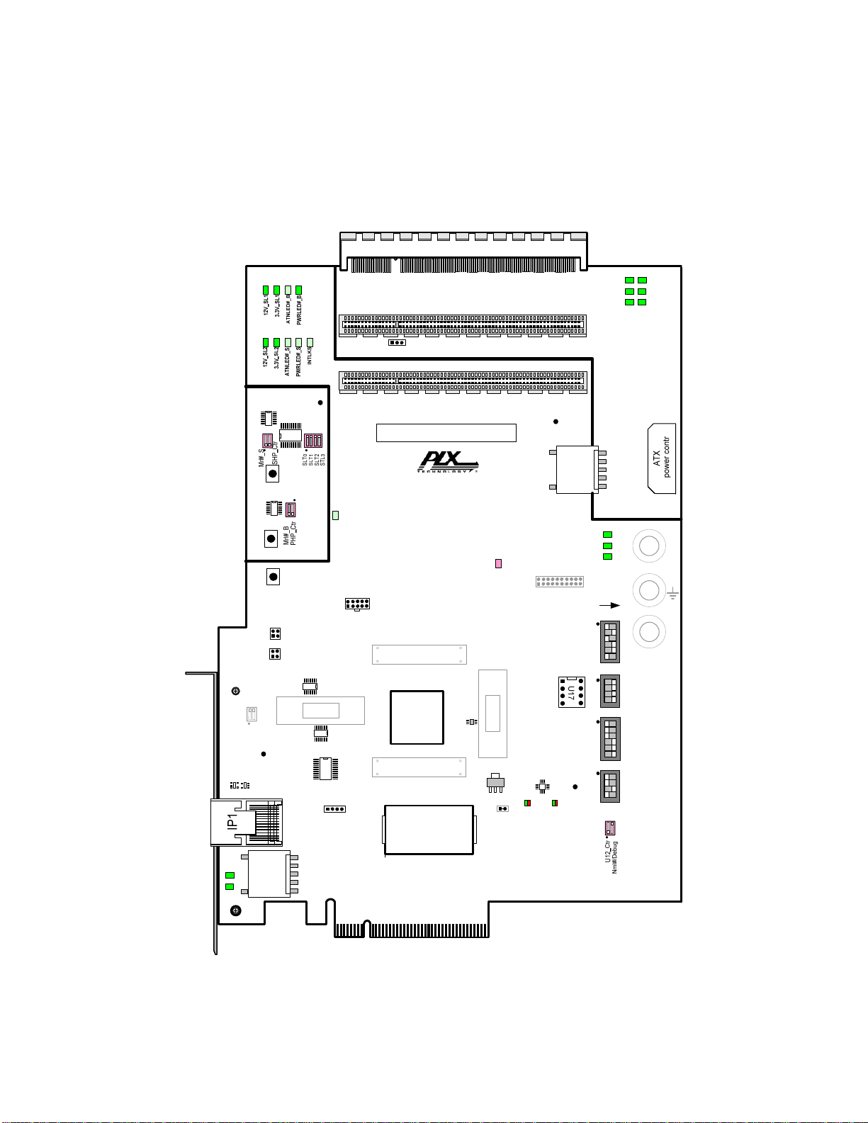
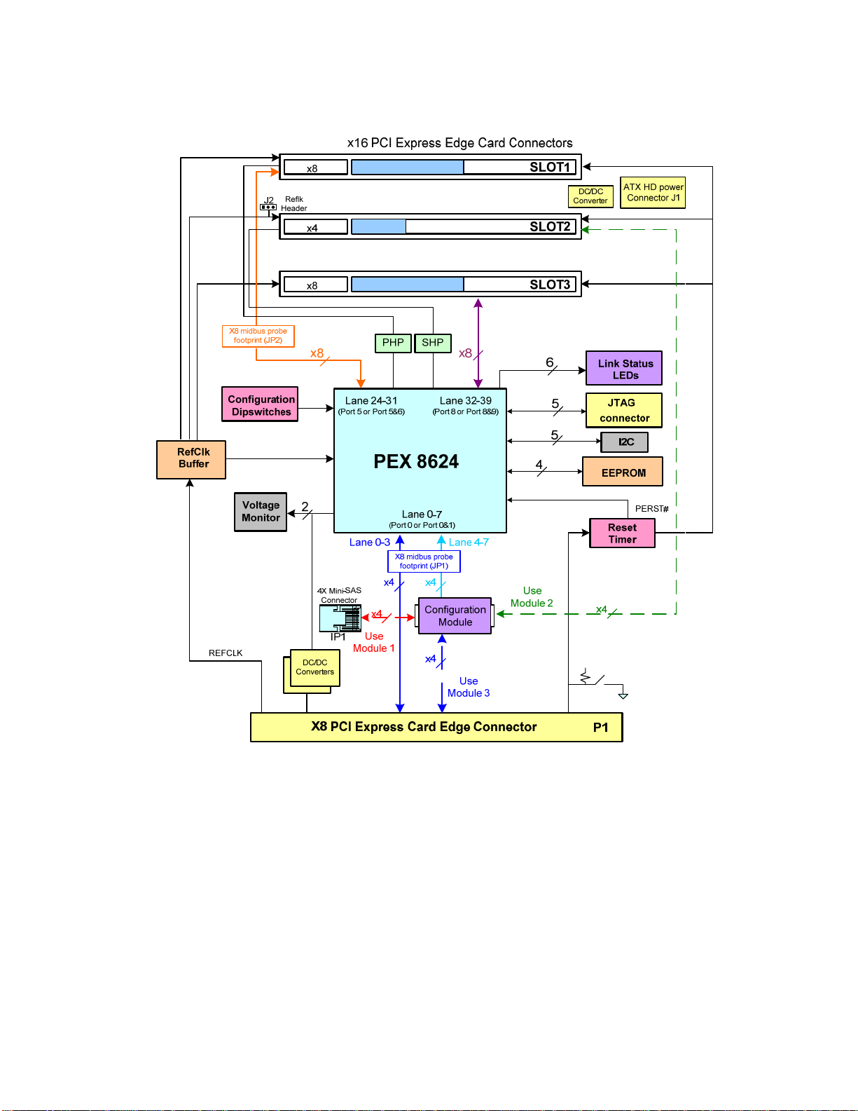
2.PEX 8624-AA RDK Hardware Architecture.......................................................................................4
2.1.1PEX 8624 PCI Express Gen 2 Switch .................................................................................. 4
2.2PEX 8624-AA RDK PCI Express Interfaces............................................................................... 4
2.2.1Configuration Modules and Receptacle CM1....................................................................... 5
2.2.2PCI Express Card Edge Connector P1.................................................................................. 6
2.2.3PCI Express Edge Card Connector SLOT 1......................................................................... 6
2.2.4PCI Express Edge Card Connector SLOT 2......................................................................... 6
2.2.5PCI Express Edge Card Connector SLOT 3......................................................................... 6
2.2.64X Mini-SAS Connector IP1................................................................................................ 6
2.3Reference Clock Circuitry............................................................................................................ 7
2.4Reset Circuitry.............................................................................................................................. 8
2.5Hot-Plug Circuits.......................................................................................................................... 8
2.5.1Parallel Hot-Plug Controller Circuit..................................................................................... 8
2.5.2Serial Hot-Plug Controller Circuits ...................................................................................... 9
2.6Serial EEPROM ......................................................................................................................... 10
2.7I2C Interface ............................................................................................................................... 10
2.8Power Distribution ..................................................................................................................... 11
2.9LED Indicators........................................................................................................................... 11
2.9.1Port Link Status Indication (D17 – D22)............................................................................ 12
2.9.2Fatal Error Indication (D24) ............................................................................................... 12
2.9.3PEX_INTA Interrupt Indication (D23)............................................................................... 12
2.9.4PEX 8624 Voltage Level Monitoring (D10 – D11)............................................................ 13
2.10GPIO Pins............................................................................................................................... 13
2.11Reserved Pins ......................................................................................................................... 13
3.On-Board Connectors, Switches, and Jumpers..................................................................................14
3.1DIP Switches.............................................................................................................................. 14
3.1.1Slot ID Selection (SW1) ..................................................................................................... 14
3.1.2Serial Hot-Plug Signal and Control (SW2)......................................................................... 14
3.1.3Parallel Hot-Plug Signal and Control (SW3)...................................................................... 15
3.1.4DC/DC Converter and Mode Controls (SW4).................................................................... 15
3.1.5Upstream Port Select (SW5)............................................................................................... 16
3.1.6Port Configuration and NT Upstream Port Select (SW6)................................................... 16
3.1.7Test Mode Select (SW7)..................................................................................................... 17
3.1.8I2C Address and Other Mode Select (SW8) ....................................................................... 18
3.2Push-Button Switches ................................................................................................................ 19
3.2.1Manual Reset# (S1)............................................................................................................. 19
3.2.2Serial Hot-Plug Controller Attention Button (S2).............................................................. 19
3.2.3Parallel Hot-Plug Controller Attention Button (S3) ........................................................... 19
3.3Midbus probe footprints (JP1 – JP2).......................................................................................... 19
3.42.5V Header (JP3)...................................................................................................................... 21
3.5JTAG Header (JP4).................................................................................................................... 21

PEX 8624-AA RDK Hardware Reference Manual – Version 1.1
Copyright © 2010 by PLX Technology, Inc. All rights reserved iii
3.6I2C Port (JP5 – JP6).................................................................................................................... 21
3.7ATX HD Power Connector (J1)................................................................................................. 22
3.8Reference Clock Header (J2) ..................................................................................................... 22
3.9Probe Mode Input Header (J3)................................................................................................... 22
3.10PLX Use Header (J4).............................................................................................................. 23
4.Bill of Materials/ Schematics.............................................................................................................24
FIGURES
Figure 1-1. PEX 8624-AA RDK Front View ............................................................................................. 1
Figure 2-1. PEX 8624-AA RDK Hardware Architecture........................................................................... 4
Figure 2-2. PCI Express up to 5GT/s Gen 2 Connections.......................................................................... 5
Figure 2-3. Use mini-SAS Connector for NT Function Setup.................................................................... 7
Figure 2-4. PEX 8624-AA RDK Reference Clock Circuit......................................................................... 7
Figure 2-5. PEX 8624-AA RDK Reset Circuit........................................................................................... 8
Figure 2-6. PEX 8624-AA RDK PHP Circuits........................................................................................... 9
Figure 2-7. PEX 8624-AA RDK SERIAL HOT-PLUG Circuits............................................................. 10
Figure 2-8. PEX 8624-AA RDK Power Subsystem................................................................................. 11
Figure 3-1. Switch SW1 Default Settings................................................................................................. 14
Figure 3-2. Switch SW2 Default Settings................................................................................................. 14
Figure 3-3. Switch SW3 Default Settings................................................................................................. 15
Figure 3-4. Switch SW4 Default Settings................................................................................................. 15
Figure 3-5. Switch SW5 Default Settings................................................................................................. 16
Figure 3-6. Switch SW6 Default Settings................................................................................................. 16
Figure 3-7. Switch SW7 Default Settings................................................................................................. 17
Figure 3-8. Switch SW8 Default Settings................................................................................................. 18
Figure 3-9. Midbus 2.0 footprint Dimensions, pin numbering and specification
(Copied from Agilent’s document).................................................................................................... 20
TABLES
Table 2-1. PEX 8624-AA RDK LED Indicator descriptions ................................................................... 11
Table 2-2. Port Link Status LED Functions.............................................................................................. 12
Table 2-3. Voltage Level Monitoring LED Functions.............................................................................. 13
Table 2-4. Strap_Reserved Pin Connections ............................................................................................ 13
Table 3-1. Switch SW2 Description ......................................................................................................... 14
Table 3-2. Switch SW3 Description ......................................................................................................... 15
Table 3-3. Switch SW5 Description ......................................................................................................... 16
Table 3-4. Switch SW6 Description ......................................................................................................... 17
Table 3-5. Switch SW7 Description ......................................................................................................... 18
Table 3-6. Switch SW8 Description ......................................................................................................... 18
Table 3-7. Signal Names of x8 PCI Express Midbus probe footprint...................................................... 20
Table 3-8. Midbus probe footprints VS. Lanes of PEX 8624................................................................... 21
Table 3-9. Pin assignment of JP4.............................................................................................................. 21
Table 3-10. Pin assignment of JP5 and JP6.............................................................................................. 21
Table 3-11. Pin assignment of J1.............................................................................................................. 22
Table 3-12. Pin assignment of J2.............................................................................................................. 22
Table 3-13. Pin assignment of J3.............................................................................................................. 22
Table 3-14. Pin assignment of J4.............................................................................................................. 23


PEX 8624-AA RDK Hardware Reference Manual – Version 1.1
Copyright © 2010 by PLX Technology, Inc. All rights reserved 1
1. General Information
The PLX PEX 8624-AA RDK is a Rapid Development Kit based on the PEX 8624, a 24-lane, 6-port PCI Express
Gen 2 switch. The PEX 8624-AA RDK provides a complete hardware and software development platform that
facilitates getting designs up and running quickly, lowering risk and reducing time-to-market. This RDK allows the
upstream port of the PEX 8624 to be directly plugged into a system board’s x8 or x16 PCI Express connector, or
plugged into an x4/x1 PCI Express connector by using card edge adapters.
Figure 1-1. PEX 8624-AA RDK Front View
1V
P1
Manual
Reset JTAG port
EEPROM
PEX 8624
(U1)
PORT 8 (X8)
SLOT 3
PORT 5 (X8)
PORT 1 (X4)
SLOT 1
SLOT 2
PORT 5
PEX 8624RDK
Configuration Module
B1
B13A13
A1
1
2
MC1
MC2
1
2
J3
JP1
Lanes 0-7
JP2
Lanes 24-31
PORT 6
D18 D17
PORT 8 PORT 9
D21 D22
PORT 0 PORT 1
D19 D20
D8 D9 D6 D7
D1 D2 D3D4 D5
U11
J1
BJ3
BJ2
BJ1
2.5V
BJ5
BJ3
SW6
SW5
SW8
SW7
U12
1
1
U5
U3
SW1
U7
SW3
on
on
on
on
ON
SW2
ON ON
U13
U10
D11
1.0V
pwrgd
D10
2.5V
pwrgd ON
SW4
JP3
J4
JP4
U2
U8 U9
SW9
ON
1
2
1
2
I2C ports
JP6
JP5
S1
S2
Button#_S
S1
Button#_B
U14
U15
U16
USPT_SEL0
USPT_SEL1
USPT_SEL2
USPT_SEL3
STN0_PCFG1
STN1_PCFG0
STN2_PCFG1
NT_USPT_SEL0
NT_USPT_SEL1
NT_ENABLE#
TMODE0
TMODE1
TMODE2
TMODE3
SERDES_MODE#
PROBE_MODE#
RSV_17#
I2C_ADD0
I2C_ADD1
I2C_ADD2
Probe Mode
Header
Power provided by J1
12V_A
5V_A
3.3V_A
D12
D14
D16
12VCC
3.3VCC
D15
D13
D23
INTA#
D24
F_ERR#
GND
GND
GND
GND
To Logic “0”
Hot Plug
1
1
1
1
PLX Technology Inc. Copyright 2008
J2

PEX 8624-AA RDK Hardware Reference Manual – Version 1.1
Copyright © 2010 by PLX Technology, Inc. All rights reserved 2
1.1 PEX 8624 Features
24-lane, 6-port PCI Express Gen 2 switch with integrated on-chip SerDes
240 GT/s aggregate bandwidth (5.0GT/s/Lane x 24 Lanes x 2 (full duplex))
19mm2324-ball Flip-Chip Plastic Ball Grid Array (FCBGA) package
Typical Power – 3.01 W
Cut-Thru packet latency of less than 150ns (x8 to x8)
Low power SerDes (under 90mW per lane)
Fully non-blocking switch architecture
Flexible port configuration
oPorts configurable as x8 or x4, with auto link-width negotiation to x2 and x1
Flexible device configuration
oConfigurable via serial EEPROM, I2C, hardware strapping, or by the host
Maximum packet payload size of 2,048 bytes
Designate any Port as the Upstream Port (Port 0 is recommended)
Dynamic Buffer Pool Architecture
Read Pacing (allows user to throttle Read requests from Downstream Ports to allow for more efficient
performance)
Dual casting (enhances performance by sending date from one ingress port to two egress ports)
Dynamic speed (2.5 GT/s or 5.0 GT/s) negotiation
Dynamic link-width negotiation (automatically negotiates down to optimal link-width based on traffic
density)
Lane and polarity reversal
Non-Transparent Bridging support
oEnables Dual-Host, Dual-Fabric, Host-Failover applications
Conventional PCI-compatible Link Power Management states – L0, L0s, L1, L2/L3 Ready, and L3 (with
Vaux not supported)
Conventional PCI-compatible Device Power Management states – D0 and D3hot
Active State Power Management
Quality of Service (QoS)
oOne Virtual Channels (VC0) and Eight Traffic classes (TC)
oRound-Robin and Weighted Round-Robin Port arbitration
Reliability, Availability, Serviceability (RAS) features
oPCI Express Standard Hot-Plug Controller for three Ports, include optional usage models for
Manually operated Retention Latch, by way of MRL Sensor and Attention Button support
oElectromechanical Interlock supported with Power Enable output
oBaseline and Advanced Error Reporting capability
oPerformance Monitoring
Per-Port Payload and Header Counters
Per-traffic type (write, Read, Completion) Counters
oJTAG AC/DC boundary scan
o6-port link status indicators (PEX_PORT_GOOD[9,8,6,5,1,0]#)
o14 GPIO and/or Serial Hot-Plug PERST# pins
INTA# (PEX_INTA#) and FATAL ERROR (FATAL_ERR#) (Conventional PCI SERR# equivalent) ball
support
Compliant to the following specifications:
oPCI Local Bus Specification, Revision 3.0 (PCI r3.0)
oPCI Bus Power Management Interface Specification, Revision 1.2 (PCI Power Mgmt. r1.2)
oPCI to PCI Bridge Architecture Specification, Revision 1.2 (PCI-to-PCI Bridge r1.2)
oPCI Express Base Specification, Revision 1.1 (PCI Express Base r1.1)
oPCI Express Base Specification, Revision 2.0 (PCI Express Base r2.0)
oPCI Express Card Electromechanical (CEM) Specification, Revision 2.0
oPCI ExpressCard CEM r2.0)
oPCI Express Mini Card Electromechanical (CEM) Specification, Revision 1.1
(PCI ExpressCard Mini CEM r1.1)
oIEEE Standard 1149.1-1990, IEEE Standard Test Access Port and Boundary-Scan Architecture,
1990 (IEEE Standard 1149.1-1990)

PEX 8624-AA RDK Hardware Reference Manual – Version 1.1
Copyright © 2010 by PLX Technology, Inc. All rights reserved 3
oIEEE Standard 1149.1a-1993, IEEE Standard Test Access Port and Boundary-Scan Architecture
oIEEE Standard 1149.1-1994, Specifications for Vendor-Specific Extensions
oIEEE Standard 1149.6-2003, IEEE Standard Test Access Port and Boundary-Scan Architecture
Extensions (IEEE Standard 1149.6-2003)
oThe I2C-Bus Specification, Version 2.1 (I2C Bus v2.1)
1.2 PEX 8624-AA RDK Features
PLX PEX 8624 PCI Express switch in a 324-ball Flip-Chip Plastic BGA package
Form factor based on PCI Express Card Electromechanical (CEM) Specification 2.0
Ships with default configuration of three x8 Ports
oAll PEX 8624 lane/port configurations supported with breakout boards and configuration modules
Non-Transparent Bridging support
Two x8 Gen 2 Midbus probe footprints for one upstream and one downstream port PCI Express signal
probing
On-board PCI Express RefClk buffer which supports Spread Spectrum Clocking
Parallel Hot-Plug and Serial Hot-Plug circuits
Socketable Serial EEPROM (2.5V)
Two standard 2x2 headers provides the I2C interface to an I2C master
DIP switches for port configuration, upstream port or NT port select and I2C address settings
Manual push-button PERST# capability
Up to six Lane Status indicator LEDs for visual inspection of link speed and status
Voltage level monitoring circuit for 1.0V and 2.5V power to the PEX 8624

PEX 8624-AA RDK Hardware Reference Manual – Version 1.1
Copyright © 2010 by PLX Technology, Inc. All rights reserved 4
2. PEX 8624-AA RDK Hardware Architecture
Figure 2-1. PEX 8624-AA RDK Hardware Architecture
2.1.1 PEX 8624 PCI Express Gen 2 Switch
The PEX 8624 is a 24-lane, 6-port PCI Express Gen 2 (5.0GT/s) switch. It is designed with three stations, with
each station housing eight lanes. Station 0 contains lanes 0 thru 7, Station 1 contains lanes 24 thru 31, and
Station 2 contains lanes 32 thru 39. Each station can be configured as one x8 port or two x4 ports. Each port can
then auto-negotiate its link-width down to x2 or x1.
2.2 PEX 8624-AA RDK PCI Express Interfaces
The PEX 8624-AA RDK is designed around the PEX 8624, a 6-port, 24-lane Gen 2 switch, and is based on the
form factor specified in the PCI Express CEM 2.0 Specification. The PEX 8624-AA RDK offers five PCI Express
(PCIe) interfaces: a x8 PCI Express Card Edge connector (P1), three x16 PCI Express Edge Card connectors
(SLOT 1, SLOT 2, & SLOT 3), and a 4X Mini-SAS connector (IP1).

PEX 8624-AA RDK Hardware Reference Manual – Version 1.1
Copyright © 2010 by PLX Technology, Inc. All rights reserved 5
Although the three PCIe slots (SLOT 1-3) have a x16 link-width form factors, the slots themselves are configured
as x8 for SLOTs 1 & 3, and x4 for SLOT 2 as shown in Figure 2-1 above. Using a x8-to-x4x4 Breakout Board, the
x8 slots (SLOTs 1 & 3) can be broken out into two x4 slots, creating two x4 ports from a x8 slot.
Port 8 or
Port 8&9
SLOT1
Port 5 or
Port 5&6
SLOT2
x8
Lane 24-31
x8
PEX 8624
(U1)
x16 PCI Express Edge Card Connectors
Downstream
Ports
Upstream Port
P1
X8 PCI Express Card Edge Connector
Lane0-3
Lane24-31
SLOT3
Lane4-7
Configuration
Module
Receptacle
x4
IP1
x4
x4
x4
x4
To upper 4
lanes of Port 0
Port 1
Port 1
Lane 0-3
A1
3
2
1
1
2
3
x8
x8
x4
X8 midbus probe
footprint (JP2)
X8 midbus probe
footprint (JP1)
4X Mini-SAS
Connector
Port 0 or
Port 0&1
Lane 32-39
Lane 4-7
Figure 2-2. PCI Express up to 5GT/s Gen 2 Connections
2.2.1 Configuration Modules and Receptacle CM1
Configuration Module Receptacle CM1 is a 200-pin high-speed Mezzanine Connector. It is soldered on the PCB
of PEX 8624-AA RDK. It directly connects to lane 4 to lane 7 of the PEX 8624, lane 4 to lane 7 of PCI Express
card edge connector P1, lane 0 to lane 3 of PCI Express Edge Card Connector SLOT 2, and lane 0 to lane 3 of
4x mini-SAS connector IP1.
One of three configuration modules (see Figure 2-2) can be plugged into the Configuration Module Receptacle
(CM1) of the PEX 8624-AA RDK. Which Configuration Module is used determines how lanes 4-7 of the PEX 8624
are routed:
1) Configuration Module 1 (marked “Enable Cable IP1”) routes lanes 4-7 to the 4X Mini-SAS Connector.
2) Configuration Module 2 (marked “Enable SLOT 2” routes lanes 4-7 to PCIe SLOT 2.
3) Configuration Module 3 (marked “Enable P1 as x8”) routes lanes 4-7 to the x8 PCIe Card Edge
Connector to enable P1 as a x8 Port.

PEX 8624-AA RDK Hardware Reference Manual – Version 1.1
Copyright © 2010 by PLX Technology, Inc. All rights reserved 6
Figure 2-2 shows the RDK PCI Express Gen 2 connections and the top view of the three configuration modules.
By default, PEX 8624-AA RDKs are shipped to customers with Configuration Module 3, enabling three x8 ports.
To achieve other configurations, a combination of x8-to-x4x4 Breakout Boards and/or Configuration Modules 1 or
2 will be required.
2.2.2 PCI Express Card Edge Connector P1
Card Edge Connector P1 can directly plug into a x8 or x16 PCI Express slot. Lanes 0-3 of PEX 8624’s Port 0 is
connected to this connector through a x8 midbus probe footprint (JP1). PEX 8624’s lanes 4-7 also passes through
the x8 midbus probe footprint (JP1) and connects to the CM1 receptacle. When Configuration Module 3 is
plugged into the CM1 receptacle, the PEX 8624’s lanes 4-7 are routed to Connector P1 and become the upper
four lanes of Port 0’s x8 link. By default, the PEX 8624-AA RDK sets this port to be the upstream port. Connector
P1 also provides 12V and 3.3V power, along with PERST# and REFCLK_P/N to the RDK.
2.2.3 PCI Express Edge Card Connector SLOT 1
Connector SLOT 1 is a straddle-mount, x16 PCI Express connector. Cards plugging into this slot will be in-line
with the RDK. Eight lanes, lanes 24-31, from the PEX 8624 are connected to this connector. The default
configuration of the PEX 8624-AA RDK sets the x8 link, Port 5, at this connector to be a downstream port. With a
x8-to-x4x4 breakout board plugged into the connector, the x8 link at port 5 can be split into two x4 links, Port 5
and Port 6. Power is provided to this connector from the ATX hard disk power connector J1 through the power
MOSFETs which are controlled by the Parallel Hot-Plug Controller (PHPC) of PEX 8624 (see Section 2.5.1 for
details).
2.2.4 PCI Express Edge Card Connector SLOT 2
Connector SLOT 2 is a vertical-mount through-hole x16 PCI Express connector. Cards plugging into this slot will
be perpendicular to the RDK. When Configuration Module 2 is plugged into the CM1 receptacle, lanes 4-7 from
the PEX 8624 pass the midbus probe footprint JP1 and CM1 and connects to Lane 0 to lane 3 of this connector.
Depending on the port configuration, port 1 at connector SLOT 2 can be a downstream port, upstream port or an
NT port. Power is provided to this connector from the ATX hard disk power connector J1 through the power
MOSFETs which are controlled by the Serial Hot-Plug Controller of the PEX 8624 (see Section 2.5.2 for details).
2.2.5 PCI Express Edge Card Connector SLOT 3
Connector SLOT 3 is a vertical-mount through-hole x16 PCI Express connector. Cards plugging into this slot will
be perpendicular to the RDK. Eight lanes, lanes 32-39, from PEX 8624 are connected to this connector. The
default configuration of the PEX 8624-AA RDK sets the x8 link, Port 8, at this connector to be a downstream port.
With a x8-to-x4x4 breakout board plugged into this connector, the x8 link can be split into two x4 links, Port 8 and
Port 9. Power is provided to this connector from the PCI Express card edge connector P1.
2.2.6 4X Mini-SAS Connector IP1
PEX 8624 only supports Non-Transparent (NT) mode on Port 0 or Port 1 of Station 0. The 4X mini-SAS connector
IP1 provides the simplified connections for the customers to connect the PEX 8624-AA RDK to two PC
motherboards. When the Configuration Module 1 is plugged into the CM1 receptacle, lanes 4-7 from the PEX
8624 pass the midbus probe footprint JP1 and CM1 and connects to the 4X mini-SAS connector IP1. Depending
on the port configuration, Port 1 at connector IP1 can be set as a downstream port, upstream port or an NT port.
Figure 2-3 shows a set up using PEX 8624-AA RDK’s NT function. Either Motherboard A or B can be connected
to an upstream port or NT port of the PEX 8624.

PEX 8624-AA RDK Hardware Reference Manual – Version 1.1
Copyright © 2010 by PLX Technology, Inc. All rights reserved 7
Figure 2-3. Use mini-SAS Connector for NT Function Setup
2.3 Reference Clock Circuitry
The PEX 8624-AA RDK reference clock circuitry contains a one-to-four differential clock fan out buffer (U2) from
SpectraLinear (CY28400-2). The clock fan out buffer supports four 100 MHz PCI Express reference clocks with
the option for constant frequency and spread spectrum outputs. When the RDK is plugged into a PCI Express slot
of a PC motherboard, the differential reference clock input to the fan out buffer is taken from the PCI Express
card-edge connector (P1), and the differential clock outputs are distributed to the PEX 8624 reference clock input
(PEX_REFCLKP/PEX_REFCLKN), downstream slot connectors (SLOT 1, SLOT 2 and SLOT 3), and the
reference clock header J2. The 3-pin reference clock header (J2) provides a reference clock input which is to be
used in conjunction with the midbus probe(s). The reference clock outputs from the fan out buffer (U2) to SLOT1
and SLOT 2 are controlled by the parallel Hot-Plug circuit and the Serial Hot-Plug circuit respectively. (See Figure
2-4 and Section 2.5 for details)
Figure 2-4. PEX 8624-AA RDK Reference Clock Circuit

PEX 8624-AA RDK Hardware Reference Manual – Version 1.1
Copyright © 2010 by PLX Technology, Inc. All rights reserved 8
2.4 Reset Circuitry
The PEX 8624-AA RDK reset circuitry includes a MAX6420 adjustable reset timer (U9), a Fairchild 2-input AND
gate NC7S08 (U8) and manual reset push-button switch (S1). The reset timer accepts PERST# from the card
edge (P1) and from S1 (logical-OR via U8). The MAX6420 has the capability of adjusting the reset timeout period
by changing the value of C70 (0.001F ≈3ms). (See Figure 2-5 for details)
Figure 2-5. PEX 8624-AA RDK Reset Circuit
2.5 Hot-Plug Circuits
PEX 8624 provides on-chip Parallel Hot-Plug controllers to downstream ports 1, 5 and 9. The remaining
downstream ports are also Hot-Plug capable through the use of the I2C bus and external I/O expander devices.
The PEX 8624-AA RDK implements Hot-Plug control circuitry for SLOT 1 and SLOT 2. SLOT 1 uses the on-chip
parallel Hot-Plug controller while SLOT 2 uses the Serial Hot-Plug control capability through the I2C and I/O
expander. Note that additional device configuration should be required when using the Serial Hot-Plug capability.
(See Section 2.5.2 and PEX 8624-AA Data Book for details)
2.5.1 Parallel Hot-Plug Controller Circuit
PEX 8624-AA RDK uses the Parallel Hot-Plug controller on Port 5 for PCI Express connector SLOT 1. The
parallel hot-plug controller consists of five input elements (HP_BUTTON_B#, HP_MRL_B#, HP_PRSNT_B#,
HP_PWR_GOOD_B, HP_PWRFLT_B#) and five output elements (HP_ATNLED_B#, HP_CLKEN_B#,
HP_PERST_B#, HP_PWREN_B, HP_PWRLED_B#).

PEX 8624-AA RDK Hardware Reference Manual – Version 1.1
Copyright © 2010 by PLX Technology, Inc. All rights reserved 9
PCI
Express
SLOT 1
VCC
System
power
supply
12V, 3.3V
VCC
VCC
Hot plug
controller
FETs
Hp_clken_b#
Hp_atnled_b#
Hp_pwrled_b#
Hp_pwren_b
Hp_perst_b#
Hp_button_b#
Hp_pwrflt_b#
Hp_mrl_b#
Hp_prsnt_b#
Hp_pwr_good_b
S2
D6 D7
TPS2311
(U6)
Pos1/SW3
Quad
2-to-1
Mux
(U7)
SN74LVC157
x8
Pwren
Perst#
Refclk
From refclk
buffer (U2)
Refclk
VCC
Pos2/SW3
HP_SL1_CTL
PEX 8624
(U1) 3.3V_SL1
D8
12V_SL1
D9VCC VCC
VCC VCC
Refclk
Buffer
Clken#
Figure 2-6. PEX 8624-AA RDK PHP Circuits
Figure 2-6 shows the parallel hot-plug circuit. It includes a low cost TI dual hot–swap power controller TPS2311
(U6), a quad 2-to-1 multiplexer SN74LVC157 (U7), two International Rectifier power MOSFET IRF7470 (Q3 and
Q4), LEDs, manual switch, dipswitch and resistors. The manual switch (S1) connects to the HP_BUTTON_B#
input of the PEX 8624. It is used to generate the active low Hot-Plug attention button signal to the parallel hot-plug
controller. LEDs D6 and D7 represent the HP_ATNLED_B# (the attention LED) and HP_PWRLED_B# (power
LED) respectively on the parallel hot-plug controller. The PRSNT2# signal from SLOT 1 connects to the
HP_PRSNT_B# signal on the parallel hot-plug controller. This signal is used to detect when a PCI Express
adapter card is plugged into the connector SLOT 1. SW3 (position 1) is used to emulate the manually operated
retention latch sensor input HP_MRL_B# to the parallel hot-plug controller. When set to “ON” position, the internal
state machine of the parallel hot-plug controller is enabled. SW3 (position 2) is used to enable the power and
clock to SLOT 1. When set to the “ON” position, the active low signal HP_SL1_CTL on the multiplexer (U7) will
select HP_PWREN_B# to enable the hot-swap power controller (U6), HP_CLKEN_B# to enable the RefClk output
to connector SLOT 1, and the reset signal HP_PERST_B# to connector SLOT 1. Inversely when set to the “OFF”
position (SW3 position 2), the active high signal HP_SL1_CTL will bypass the Hot-Plug control outputs from the
parallel hot-plug controller and select another set of outputs to enable the hot-swap power controller (U6), and
enable the RefClk output and PERST# to connector SLOT 1.
When enabled, the hot-swap power controller (U6) monitors the 12V and 3.3V voltage supplies to SLOT 1. When
current levels exceed 5A, HP_PWRFLT# becomes active. Similarly, HP_PWR_GOOD_B becomes active when
lower than normal current levels are detected. PWRGD1 and PWRGD2 implement pull-up with external resistor.
Two additional LEDs, D8 and D9, are used to indicate 3.3V and 12V power at the connector SLOT 1.
2.5.2 Serial Hot-Plug Controller Circuits
PEX 8624-AA RDK also implements the serial hot-plug controller circuitry to PCI Express SLOT 2. By default, the
RDK is configured to bypass the serial hot-plug controller. In order to configure port 1 at PCI Express SLOT 2 as
a Serial Hot-Plug port with the port 0 is still a x4 upstream port, use the EEPROM to write 2’b00 to the bit [14:13]
of station 0’s Parallel Hop-Plug capable configuration register at offset 1E0h.

PEX 8624-AA RDK Hardware Reference Manual – Version 1.1
Copyright © 2010 by PLX Technology, Inc. All rights reserved 10
x4
Figure 2-7. PEX 8624-AA RDK SERIAL HOT-PLUG Circuits
The serial hot-plug controller consists of an I/O expander (MAX 7311 (U3)), a dual hot–swap power controller
(TPS2311 (U4)), a quad 2-to-1 multiplexer (SN74LVC157 (U5)), two power MOSFET IRF7470 (Q1 and Q2),
LEDs, manual switch, dipswitches and resistors. The PEX 8624 master I2C interface is designed for the specific
control use of the serial hot-plug controller. The master I2C interface connected to the I/O expander and the
interrupt output from the I/O expander connects to the SERIAL HOT-PLUGC_INT# of the PEX 8624. When power
is applied to the PEX 8624, the master I2C interface will scan the bus and attempts to detect the presence of the
I/O expander. If an I/O expander is detected, the I2C master will program it as a “remote parallel hot-plug
controller” and assign an available serial hot-plug port to the I/O expander. (see Section 2.5.1, Figure 2-6 and
Figure 2-7 for details).
The RDK also provides dipswitches for setting the SLTID [3:0], a test point for access the GPIO pin, and three
pull-down resistors to set AD [2:0] of the I/O expander U3. The LEDs D1 and D2 are 12V and 3.3V power
indicators when power reaches PCI Express connector SLOT 2.
2.6 Serial EEPROM
The PEX 8624-AA RDK contains an 8-pin DIP socket for a serial EEPROM (U17). The board is populated with a
blank On Semi CAT25080LI-G 32-Kbit device. The CAT25080LI-G device can directly interface to the PEX8624.
When programmed correctly, the serial EEPROM can be used to change the default configuration of the PEX
8624. A blank EEPROM results in the default register values set in the PEX 8624. Please refer to the Software
Development Kit (SDK) documentation for additional information on how to program the serial EEPROM.
2.7 I2C Interface
The PEX 8624 implements an I2C slave interface (I2C port 0), which allows an external I2C master to read and
write device registers through an out-of-band mechanism. The PEX 8624 I2C interface is accessible via a 7-bit
address, at data rates from 100 Kbps up to 3.4 Mbps. The RDK provides two cascaded 2x2, 0.1” pitch headers
(JP5 and JP6), which interface to the PEX 8624’s I2C port. That allows for cascading multiple RDKs together
using standard ribbon cable, and/or connecting to an I2C master such as the Total Phase Aardvark I2C controller.
(See Section 3.6 for pin assignment of JP5 and JP6.)

PEX 8624-AA RDK Hardware Reference Manual – Version 1.1
Copyright © 2010 by PLX Technology, Inc. All rights reserved 11
2.8 Power Distribution
The PEX 8624-AA RDK has two sources of DC power. The first source is the card edge connector (P1). The x8
connector provides up to 2.1A at 12V and 3.0A at 3.3V from the PCI Express edge card connector it plugs in. The
power from P1 is intended to power the PEX 8624, PCI Express connector SLOT 2, and the on-board electronic
components. The dc/dc converter U12 converts 12V from the Card Edge connector to 1.0VCC to support the
SerDes and core power of the PEX 8624. The LDO U13 converts 3.3V to 2.5VCC to support the I/O power of the
PEX 8624.
The second source of power includes an ATX HD power connector J1, and a 5V to 3.3V step down dc/dc
converter U11. Through controlled power MOSFETS, connector J1 provides 12VCC up to 5A to each of PCI
Express Edge Card Connectors SLOT 1 and SLOT 2. The J1 also provides enough 5V power for the dc/dc
converter U11 to generate 3.3VCC up to 3A for each of SLOT 1 and SLOT 2 (See Figure 2-8 for details).
12V_A
5V_A
Figure 2-8. PEX 8624-AA RDK Power Subsystem
2.9 LED Indicators
The PEX 8624-AA RDK provides a number of LED indicators including power-on indication, PEX 8624 port link
status indication, Hot-Plug LED indication, fatal error indication, event/error indication, and voltage level
monitoring indications. Table 2-1 provides a quick explanation of the various board indicators.
Table 2-1. PEX 8624-AA RDK LED Indicator descriptions
Indicator Type Locations LED Functions
Slot Power LED/green color D1 On: 12V at PCI Express connectors SLOT 2
D2 On: 3.3V at PCI Express connectors SLOT 2
Slot Power LED/green color D8 On: 12V at PCI Express connectors SLOT 1
D9 On: 3.3V at PCI Express connectors SLOT 1
SERIAL HOT-PLUG LED/green color D3 On: HP power LED output active at port 1
D4 On: HP Attention LED output active at port 1

PEX 8624-AA RDK Hardware Reference Manual – Version 1.1
Copyright © 2010 by PLX Technology, Inc. All rights reserved 12
Indicator Type Locations LED Functions
D5 On: HP interlock output active at port 1
PHP Attention LED/green color D6 On: HP Attention LED output active at port 5
D7 On: HP power LED output active at port 5
Slot Power LED/green color D8 On: 12V at PCI Express connectors SLOT 1
D9 On: 3.3V at PCI Express connectors SLOT 1
Voltage level monitoring / bi-color LED D10 Monitor 2.5V to PEX 8624 (see Table 2-3 for details)
D11 Monitor 1V to PEX 8624 (see Table 2-3 for details)
Slot 1-2 Power LED/green color
D12 On: 12V at ATX HD power connector J1
D14 On: 5V at ATX HD power connector J1
D16 On: 3.3V at dc/dc converter U11 output
Board Power LED/green color D13 On: 12V at edge card connector P1
D15 On: 3.3V at edge card connector P1
PEX 8624 Port Link Status LED (driven by
PEX_PORT_GOOD pins) /green color
D19 Port 0 speed and link activity (see Table 2-2 for details)
D20 Port 1 speed and link activity (see Table 2-2 for details)
D18 Port 5 speed and link activity (see Table 2-2 for details)
D17 Port 6 speed and link activity (see Table 2-2 for details)
D21 Port 8 speed and link activity (see Table 2-2 for details)
D22 Port 9 speed and link activity (see Table 2-2 for details)
INTA# of PEX 8624/green color D23 On: event/error occurs
FATAL_ERR#/red color D24 On: error(s) occurs (see PEX 8624-AA Data Book)
2.9.1 Port Link Status Indication (D17 – D22)
The PEX 8624-AA RDK provides up to six green color link status LEDs, D17 to D22, to indicate its port 0, 1, 5, 6,
8 and 9 link states. LED on, off, and three blinking patterns cover all five states of port link status. (See Table 2-2
for details)
Table 2-2. Port Link Status LED Functions
Port Link State LED Pattern
Link down off
Link up, 5Gbps, all lanes are up on
Link up, 5Gbps, reduced lanes are up Blinking: 0.5 second on, 0.5 second off
Link up, 2.5Gbps, all lanes are up Blinking: 1.5 second on, 0.5 second off
Link up, 2.5Gbps, reduced lanes are up Blinking: 0.5 second on, 1.5 second off
2.9.2 Fatal Error Indication (D24)
The PEX 8624 provides an output status pin (FATAL_ERR#) which reports the event of a PCI Express fatal error
condition. The RDK connects this output to a red LED (D24) which is lit when a fatal error condition is detected.
Examples of fatal error conditions are data link layer protocol errors, receiver overflow and malformed TLPs. The
PCI Express Base specification provides a complete listing of fatal error conditions. The PEX 8624-AA Data Book
also provides additional details on the assertion of FATAL_ERR#.
2.9.3 PEX_INTA Interrupt Indication (D23)
The PEX 8624 provides an output status pin (PEX_INTA#) for signaling various programmable events. The RDK
connects this output to a green LED (D23) for this interrupt output. Please refer to the PEX 8624-AA Data Book
for additional information on the programmable events for PEX_INTA#.

PEX 8624-AA RDK Hardware Reference Manual – Version 1.1
Copyright © 2010 by PLX Technology, Inc. All rights reserved 13
2.9.4 PEX 8624 Voltage Level Monitoring (D10 – D11)
The PEX 8624-AA RDK provides voltage level monitoring circuit to monitor the 1 volt and 2.5 volt power to the
PEX 8624. The circuit contains an Intersil multiple voltage supervisory ISL6132, two bi-color LEDs, D10 and D11,
and various value resistors. When the 1 volt or 2.5 volt is within the +/- 10% range the green LED will turn on.
Otherwise the red LED will be on. (See Table 2-3 for details)
Table 2-3. Voltage Level Monitoring LED Functions
LED Green LED on/ Red LED off Green LED off/Red LED on
D8 1 volt to PEX 8624 within +/- 10% range 1 volt to PEX 8624 out of +/- 10% range
D9 2.5 volt to PEX 8624 within +/- 10% range 2.5 volt to PEX 8624 out of +/- 10% range
2.10 GPIO Pins
The PEX 8624 has fourteen GPIO pins. All GPIO pins are connected to mictor connectors (MC1 and MC2) to be
used by external applications.
2.11 Reserved Pins
The PEX 8624 has 9 STRAP_RESERVED pins. They are factory use only and should be set to know logic states.
Table 2-4 shows the list of these reserved pins and their connections in the RDK.
Table 2-4. Strap_Reserved Pin Connections
Name Pin Location Connections on PEX 8624-AA RDK
STRAP_RESERVED0 J4 Pull-down with a 1K ohm resistor
STRAP_RESERVED1 P2 Pull-down with a 1K ohm resistor
STRAP_RESERVED2 K5 Pull-up with a 4.7K ohm resistor
STRAP_RESERVED3 E2 Pull-down with a 1K ohm resistor
STRAP_RESERVED4 V12 Pull-down with a 1K ohm resistor
STRAP_RESERVED7 F3 Pull-up with a 4.7K ohm resistor
STRAP_RESERVED8 E12 Pull-down with a 1K ohm resistor
STRAP_RESERVED16 T13 Pull-down with a zero ohm resistor
STRAP_RESERVED17# D18 Set DIP switch to OFF (logic ‘HIGH’)

PEX 8624-AA RDK Hardware Reference Manual – Version 1.1
Copyright © 2010 by PLX Technology, Inc. All rights reserved 14
3. On-Board Connectors, Switches, and Jumpers
3.1 DIP Switches
The PEX 8624-AA RDK contains nine user controllable DIP switches (SW1-SW9) for selecting the slot ID for the
serial hot-plug, enable/disable Hot-Plug signals, enable/bypass the serial hot-plug and parallel hot-plug, upstream
port select, port configuration, NT upstream port select, I2C address settings and test mode settings. The
dipswitches are presented following the orientations shown in Figure 3-1.
3.1.1 Slot ID Selection (SW1)
Figure 3-1. Switch SW1 Default Settings
Switch SW1 is used to set the slot ID for the PCI Express SLOT 2. Users can select one of 16 combinations.
3.1.2 Serial Hot-Plug Signal and Control (SW2)
Figure 3-2. Switch SW2 Default Settings
Table 3-1. Switch SW2 Description
SW2 Functional Description Switch Position Settings
Enable/bypass SERIAL HOT-
PLUG outputs to generate
power, RefClk and PERST#, to
connector SLOT 2
Position 2
ON: enable SERIAL HOT-PLUG outputs to generate power, RefClk and
PERST# to SLOT 2
OFF: bypass SERIAL HOT-PLUG and still provide power, RefClk and PERST#
to SLOT 2
Enable/disable MRL#_S at
Serial Hot-Plug
Position 1
ON: enable MRL#_S
OFF: disable MRL#_S
Table of contents
Popular Industrial Equipment manuals by other brands

Spirax Sarco
Spirax Sarco UFT32 Installation and maintenance instructions

Wolf
Wolf THERM CONNECT Operation & maintenance instructions

PCB Piezotronics
PCB Piezotronics 8120-410A Installation and operating manual

altitude
altitude COMMSCOPE FIST-GCO2 Installation instruction

Nibe
Nibe ERS S10 Installer manual

Vantron
Vantron DE20-BT user manual