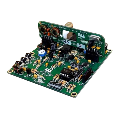
QRPGuys DSB Digital Transceiver Kit User manual

QRPGuys Digital DSB Transceiver Kit
First, familiarize yourself with the parts and check for all the components. If a part is missing, please contact us
at [email protected] and we will send you one.
Please read all the instructions before starting to assemble the transceiver.
PARTS LIST
LOCATION QUANTITY VALUE TYPE
C1, C2, C10, C16 4 10 nF - 103 X7R MMLC
C3, C6 2 100 uF /16V Long lead plus
C4, C5, C7, C8, C9, C11, C13,
C14, C15, C18, C21, C22
12 100 nF - 104 X7R MMLC
C12, C17, C20 3 1 uF / 25V Long lead plus
C19 1 1 nF - 102
D1 1 1N5817 BLACK PLASTIC
D2, D3, D4 3 1N4148 SMALL GLASS
D5 1 LED Green May have clear lens
D6 1 LED Red May have clear lens
J1 1 BNC Jack PCB MOUNT
J2 1 2.1mm DC Jack PCB MOUNT
Page 1 of 13 digital_txcvr_assembly_030720.pdf

J3, J4 2 3.5mm Phone Jack STEREO, SWITCHED
J5, J6 2 5 Position SIP Jack 0.1” CENTERS
K1 1 12V DPDT Relay
L4 1 10 uH choke Brown-black-black-gold or silver
Q1, Q2, Q3, Q4, Q5, Q6 6 BS170 TO-92 MOSFET
Q7 1 2N3904 TO-92 NPN
R1 1 51 ohms GRN-BRN-BLK-GLD
R2 1 4.7K YEL-VIO-RED-GLD
R3 1 1 MEG BRN-BLK-GRN-GLD
R4, R6 2 100K BRN-BLK-YEL-GLD
R5, R14, R16 3 1K BRN-BLK-RED-GLD
R7, R17 2 5.6 ohms GRN-BLUE-GOLD-GLD
R8, R10, R13 3 10K BRN-BLK-ORG-GLD
R9 1 470K YEL-VIO-YEL-GLD
R11 1 680K BLUE-GRY-YEL-GLD
R12 1 47K YEL-VIO-ORG-GLD
R15 1 470 ohms YEL-VIO-BRN-GLD
U1 1 SA602 / SA612A DIP 8 MIXER/OSC
U2 1 LM358 DIP 8 DUAL OPAMP
U3 1 LM7809 TO-220 9V/1A REG
V1, V2 2 6mm sq. , 2K TRIMMER RESISTOR
T1, T2 2 FT37-43 FERITE CORE, BLACK
8 PIN DIP SOCKET 2 8 Pin DIP Socket
PCB 1 Main Circuit Board
SCREW 1 4-40 1/4”
NUT 1 4-40 nut
FEET 4 Rubber Feet
BAL HEADER 1 2 position SIP pin strip
SHORTING JUMPER 1 Shorting jumper
BAND PARTS, SEE TABLE
FOR LOCATIONS
QUANTITY VALUE TYPE
CAPACITORS 6 22 pF C0G
1 33 pF C0G
1 47 pF C0G
1 68 pF COG
2 150 pF – marked 151 C0G
2 220 pF – marked 221 C0G
3 330 pF - marked 331 C0G
1 560 pF – marked 561 C0G
1 680 pF – marked 681 C0G
Page 2 of 13 digital_txcvr_assembly_030720.pdf

INDUCTORS 1 2.2 uH Red-red-gold-gold or silver
1 3.9 uH Orange-white-gold-gold or silver
1 8.2 uH Gray-red-gold-gold or silver
4 T37-2 Red Core
2 T37-6 Yellow Core
CRYSTALS 1 7.074 MHz HC-49/US
1 10.136 MHz HC-49/US
1 14.074 MHz HC-49/US
MISCELLANEOUS
3 Band module boards
12' #26 magnet wire
1' #26 magnet wire, different
color
12 3/32” tie wrap
J5,6 6 5 position 90 ° SIP pin
strip
Parts placement diagram: Print this page for quick reference
Page 3 of 13 digital_txcvr_assembly_030720.pdf

Assembly:
The first step is to sort the parts into groups of similar types. This will make finding the needed part
type and value quicker.
Start with the resistors:
Caution: Several of the values have very similar color codes and differ only by the zero
multiplier color. It is also easy to mix up the 51 and 1 Meg resistors as 51 is
green/black/brown and 1 meg is brown/black/green. L4 is a RF choke. It looks like a
resistor, but is a bit fatter. With an ohm meter, it will read 0 ohms.
[ ] R1 - 51 Green/Brown/Black/Gold
[ ] R2 - 4.7K Yellow/Violet/Red/Gold
[ ] R3 - 1 Meg Brown/Black/Green/Gold
[ ] R4, R6 - 100K Brown/Black/Yellow/Gold
[ ] R5, R14, R16 - 1K Brown/Black/Red/Gold
[ ] R7, R17 - 5.6 ohm Green/Blue/Gold/Gold
[ ] R8, R10, R13 – 10K Brown/Black/Orange/Gold
[ ] R9 – 470K Yellow/Violet/Yellow/Gold
[ ] R11 – 680K Blue/Gray/Yellow/Gold
[ ] R12 – 47K Yellow/Violet/Orange/Gold
[ ] R15 - 470 Yellow/Violet/Brown/Gold
[ ] L4 – 10 uH inductor Brown/Black/Black/Gold,
last band can be silver
[ ] D1 – 1N5817 Diode, black plastic body,
match band with outline
[ ] D2, D3, D4 – 1N4148 Diode, glass body, match
band with outline
Capacitors:
[ ] C1, C2, C10, C16 – 10 nF, 103 Orange highlight
[ ] C19 – 1 nF, 102 Red highlight
[ ] All others 100 nF, 104 – Yellow highlight 12 places
[ ] C12, C17, C20 – 1 uF – long lead is plus.
[ ] C3, C6- 100 uF – long lead is plus.
Note: When reading capacitor values, do not
confuse the manufacturing codes with the
component value. If it looks strange it may be
a manufacturing code, look on the other side of
the component. Also, the value may be
followed by a tolerance code - M,K, or J.
Page 4 of 13 digital_txcvr_assembly_030720.pdf

Everything else:
[ ] U3 – 7809 Bend the leads so that the U3 hole
lines up with the board hole. Secure with 4-40 screw
and nut.
[ ] J5, J6 – 5 pins SIP socket. Make sure these are
set square and straight to the board before soldering
more then one pin.
[ ] U1, U2 - 8 pin DIP socket. Note orientation of
notch on socket and match with notch on part board
outline. Make sure all the pins are sticking out the
solder pads before soldering any!
[ ] J3, J4 – 3.5mm phone jacks
[ ] Q1, Q2, Q5 – BS170 MOSFET Note orientation
of the flat side of part. Make sure it matches the
board outline.
[ ] Q7 – 2N3904 NPN Make sure it matches the board outline.
Note: LED's may have clear lenses. Determine which color by touching to a coin battery or similar
battery. If when completed you find the intensity is too great, change R16 to 10K or 22K.
[ ] D5 - Green LED – short lead goes into hole on flat side of part outline.
[ ] D6 – Red LED – short lead goes into hole on flat side of part outline.
[ ] V1, V2 – 2K trimmer pots
[ ] Relay – not specifically labeled, but should be obvious where it goes!
[ ] J2 – DC power Jack.
[ ] J1 – BNC antenna jack
[ ] BAL – 2 pin SIP header
[ ] BALANCE – not used. It was found this part is not necessary.
[ ] Q3, Q4, Q6 – These parts require some heat sinking. Therefore, these parts get mounted with the
flat side of the package pressed against the large, tinned pad to the left of the board. A stiff piece of
paperclip wire can be used to hold the parts down against the pad by soldering it to the two mounting
holes on either side. A better method would be to use a piece of aluminum, secured with 4-40 screws,
using the mounting holes on either side. If you have some conductive paste, use it.
Flat side down Piece of paperclip wire Opt. aluminum w/hardware
Page 5 of 13 digital_txcvr_assembly_030720.pdf

[ ] T1, T2 – bi-filler wound on T37-43 ferrite core
(black).
•Cut 6” length of each color magnet wire
•The two wires can be lightly twisted
together, but this is not necessary
•Wind 5 turns on the core as shown.
•Trim and tin the wire ends. Either
scrape or melt the insulation using a hot iron with a blob
of solder.
•Orientate the common wire ends so they are
opposite each other on the core.
•The wires will now be in the proper position for
inserting into the board.
Be sure to tin the wire ends before installing. The transceiver will not work if you do
not tin the magnet wire. This is the leading cause of failure.
[ ] Stick the rubber bumper feet on the corners of the board.
Assembling the band modules
[ ] Before populating with components, mark each module with the band and mode in the space
provided with a permanent marker.
[ ] J5,J6 – 5 pin right angle SIP header strip. Short 90° pins go into board. Mount on the top of the
board as shown. Trim the pins flush on the backside.
Use the placement graphic and tables below to install the capacitors, crystals, and inductors.
Note: When reading module capacitor values, do not confuse the manufacturing codes
with the component value. If it looks strange, it may be a manufacturing code, look on
the other side of the component.
Page 6 of 13 digital_txcvr_assembly_030720.pdf

Be sure you have read the values correctly. Sort all the capacitors out before you
start assembling them onto the modules. They are difficult to remove and correct.
40M
[ ] L1 – 8.2 uH – Gray-red-gold-gold, last band can be silver
[ ] C26 – not used
[ ] C27 – 22 pfd – marked 22, it may be followed by a letter
[ ] C28 – 22 pfd – marked 22, it may be followed by a letter
[ ] C29 – 330 pfd – marked 331
[ ] C30 – 680 pfd – marked 681
[ ] C31 – 68 pfd – marked 68, it may be followed by a letter, (don't mix up the 681 and 68 values!)
[ ] C32 – 330 pfd – marked 331
[ ] L2 – 20 turns on T37-2 RED core – make sure turns are snug to the core and more or less evenly
spaced around the core. Loose winding does not work well.
[ ] L3 – 18 turns on T37-2 RED core
[ ] X1 – 7.074 MHz crystal
30M
[ ] L1 – 3.9 uH – Orange-white-gold-gold, last band can be silver
[ ] C26 – not used
[ ] C27 – 22 pfd – marked 22, it may be followed by a letter
[ ] C28 – 22 pfd – marked 22, it may be followed by a letter
[ ] C29 – 220 pfd – marked 221
[ ] C30 – 560 pfd – marked 561
[ ] C31 – 47 pfd – marked 47, it may be followed by a letter
[ ] C32 – 220 pfd – marked 221, (don't mix up the 221 and 22 values!)
[ ] L2 – 18 turns on T37-2 RED core – make sure turns are snug to the core and more or less evenly
spaced around the core. Loose winding does not work well.
[ ] L3 – 13 turns on T37-2 RED core
[ ] X1 – 10.136 MHz crystal
20M
[ ] L1 – 2.2 uH – Red-red-gold-gold, last band can be silver
[ ] C26 – not used
[ ] C27 – 22 pfd – marked 22, it may be followed by a letter
[ ] C28 – 22 pfd – marked 22, it may be followed by a letter
[ ] C29 – 150 pfd – marked 151
[ ] C30 – 330 pfd – marked 331
[ ] C31 – 33 pfd – marked 33, it may be followed by a letter (don't mix up the 331 and 33 values!)
[ ] C32 – 150 pfd – marked 151
[ ] L2 – 17 turns on T37-6 YELLOW core – make sure turns are snug to the core and more or less
evenly spaced around the core. Loose winding does not work well.
[ ] L3 – 15 turns on T37-6 YELLOW core
[ ] X1 – 14.074 MHz crystal
Page 7 of 13 digital_txcvr_assembly_030720.pdf

Winding the toroids
[ ] Wind each of the L2 and L3 toroids using 12” of the supplied magnet wire. Use the tables above
and wind them in the direction shown in the graphic below and they will align with the pcb holes.
When you are certain of the turn count, trim the leads ~1/2” and tin them before installing the toroids
flat on the top of the board, centered on the silkscreen outline. Secure each toroid to the pcb using two
of the supplied plastic zip ties, as shown below.
Be sure to tin the wire ends before installing. The transceiver will not work if you do
not tin the magnet wire. This is the leading cause of failure.
Test and set up:
[ ] Apply 12V to 13.8V to the board. The GREEN LED should light.
[ ] Verify 9V (+/- 0.25) between pins 8 and 4 of U2. (Optional)
[ ] Remove power
[ ] Install SA602 IC into U1 socket. Observe orientation, notch on chip matches notch on IC socket.
[ ] Install LM358 IC into U2 socket. Observe orientation, notch on chip matches notch on IC socket.
[ ] Connect your DMM in series with the positive power supply lead and set the meter to measure
current. To be safe, use the 10A scale.
[ ] Set the V1 (BIAS) trimmer to fully CLOCKWISE.
[ ] Apply power to the board again.
[ ] Insert the shorting plug into the [BAL] SIP pins. This will force the board into transmit mode. The
RED LED should now be on and the GREEN LED off.
[ ] Note the amount of current the board is drawing.
[ ] Slowly adjust the V1 trimmer COUNTERCLOCKWISE while watching the current meter. Adjust
until the current goes up by about 15 ma. This is just enough to put the PA into linear mode.
[ ] Remove power.
[ ] Remove the shorting plug for the BAL pins.
If the current does not rise on counterclockwise rotation, check the connections of T2.
Operating or testing into a bad SWR or no antenna will permanently damage the
three power amplifier BS170's. Be careful...
You are now ready for on-air testing.
[ ] Start the WSJT-X program on your PC or Laptop.
[ ] Set up your computer to look for inputs and outputs at the auxiliary sound connections if needed.
[ ] Make the required MIC and Headphone connections between the PC and DSB board. MIC to MIC
and PHONES to PHONES. (I found nice stereo jumper cables at the Dollar Store).
[ ] Plug in the desired band module. The toroid side of the module faces you, the end with the LEDs.
[ ] Connect up your antenna.
[ ] Power up the board.
Page 8 of 13 digital_txcvr_assembly_030720.pdf

Note: While testing for operation, you can temporarily plug some earbuds into J3 MIC (OUT). This
is the audio out to your computer or tablet. If the particular band is open, you should hear received
signal tones in one of the earbuds. If you are not hearing any signals, determine the cause and
correct before continuing.
[ ] You should start to see signals. Adjust the Sound card input level and the V2 audio output level to
appropriate settings for your conditions.
[ ] Replace the antenna with a 50 ohm dummy load.
[ ] Set the sound card output level to minimum.
[ ] Activate “TUNE” on the WSJT-X to manually transmit.
[ ] Increase sound card output level until the board switches into Transmit. (RED LED goes on) you
can continue to increase the output level a little bit to ensure reliable triggering of the VOX circuit.
[ ] Press “TUNE” again to stop the manual transmitting mode.
If you have a watt meter in line with the antenna, you will notice the power will
continue to increase as the audio input continues to increase. Do not do this. The
apparent increase in power is due to overloading the mixer and amplifier stages,
putting them into a non-linear region.
If you look at the RF output with an Oscilloscope, it should look like a string of pearls. This is the
result of the two side bands mixing. Increasing the drive will turn the string of pearls into more of a
picket fence and then approach being a wall. This is the result of the amplifier stages saturating
resulting in the signal flat topping. At this point your creating spurious outputs to the annoyance of
others in the band. Keep it clean. It's bad enough we're transmitting two side bands.
[ ] Reconnect your antenna and you are good to go.
Refer to the WSJT-X documentation and our website links for the details on operation.
Theory of operation:
The F8 DSB transceiver is built around the ubiquitous SA602/612A mixer-oscillator chip. It provides both the
receive and transmit functions.
Receiver:
The antenna is first routed through the transmitter's Low Pass Filter (LPF) and then into the T/R relay. The
received signal is bottom coupled into the tuned circuit comprised of L1 and C26. C26 is actually the stray
capacitance of the band module and SIP connectors. Although this does not peak L1 at exactly the desired input
frequency, it's close enough as the single L/C tank circuit is pretty broad.
The received input signal is mixed with the internal oscillator, to produce the base line audio output. The audio
output is coupled to a high gain audio amplifier through two 0.1 ufd caps (C15+C13) in series. The MOSFET
Q5 is connected to the common point of C15 and C13 provides audio muting during transmit by shunting the
junction to ground.
U2b, one half of a LM358 op amp, provides audio gain for decent sensitivity. A non-inverting configuration is
used so that the input can be high impedance, allowing for reasonably small value input coupling caps. The gain
is set to 47. The amplifier then drives an audio level pot so the audio level can be adjusted to a level suitable for
your PC sound card.
Page 9 of 13 digital_txcvr_assembly_030720.pdf

Transmitter:
The SA602 requires very little input signal to saturate. Therefore a resistor divider is placed between the audio
input from the sound card to the mixer input. This allows you to set the audio output from the sound card to a
reasonable level and not overdrive the mixer.
The other half of the LM358 (U2a) is used as a VOX circuit. The peak detector circuit of D4 and C11 isn't
required for FT8 operation, but is include if one wishes to add a VFO and microphone to use the rig as a DSB
voice transceiver or possibly try PSK31. This prevents the relay from chattering.
The output of the peak detector drives three BS170 MOSFETs. Q1 activates the T/R relay. Q2 shorts out the
antenna input to the mixer, along with connecting C9 to ground to by pass the antenna input side of the mixer
input to ground. Q5 shorts the C15/C13 junction to ground for audio muting as described earlier.
One section of the DPDT T/R relay is also used to short the receiver input to ground. Keeping as much of the
transmit signal out of the mixer input as possible is important to prevent unwanted spurious outputs. The other
half of the relay routes power to the transmitter amplifiers and lights the transmit LED.
Q7 amplifies the RF output from the mixer to a level sufficient to drive the PA. The PA is comprised of three
BS170 MOSFETS in parallel. Bias is applied to the gates to place the amplifier into liner mode. This also
reduces the amount of drive needed since the input signal does not have to first exceed the ~2.5V it takes to
start to turn on the MOSFETS.
Power to the circuits is supplied by a 9V, 1A regulator. This ensures the power output remains in a safe
operating area and if there is a problem, the internal over current protection will shut down the regulator. Since
the maximum operating voltage of the SA602/612 is 9V, a diode is placed in series with the 9V supply insure
the voltage to the chip does not exceed the maximum recommended supply voltage.
Notes:
______________________________________________________
______________________________________________________
______________________________________________________
______________________________________________________
______________________________________________________
______________________________________________________
______________________________________________________
______________________________________________________
______________________________________________________
______________________________________________________
______________________________________________________
______________________________________________________
Page 10 of 13 digital_txcvr_assembly_030720.pdf
Table of contents
Other QRPGuys Transceiver manuals
