Racal Instruments 9901 User manual

9901
Universal Counter-Timer
1978
THE QUEEN'S AVMRO
FOR TECHNOLOQICAL ACHIEVEIWNT
TO DACAL DANA INSTRUMENTS LTD.
UX3BSB
The Electronics Group
Racal-Dana Instruments Limited Duke Street, Windsor, Berks, England
Prepared by Central Handbooks Department, Racal Group Services Limited.
Printed in England Ref. WOH 6201 Issue 7.2.79-150

LETHAL WARNING
Voltages within this equipment are sufficiently
high to endanger life.
Covers are NOT to be removed except by persons
qualified and authorised to do so and these
persons should always take extreme care
once the covers have been removed.
Resuscitation instructions are given overleaf.

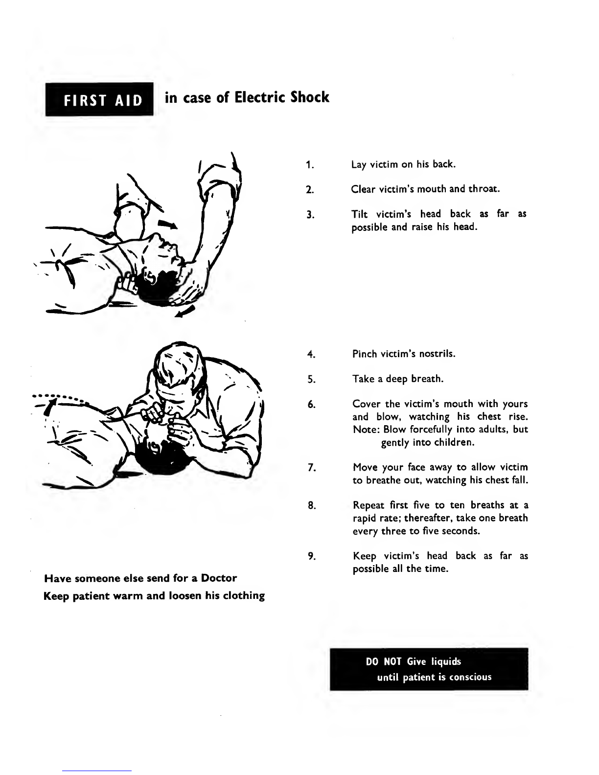
FIRST AID in case of Electric Shock
1. Lay victim on his back.
2. Clear victim’s mouth and throat.
3. Tilt victim’s head back as far as
possible and raise his head.
Have someone else send for aDoctor
Keep patient warm and loosen his clothing
4. Pinch victim’s nostrils.
5. Take adeep breath.
6. Cover the victim’s mouth with yours
and blow, watching his chest rise.
Note: Blow forcefully into adults, but
gently into children.
7. Move your face away to allow victim
to breathe out, watching his chest fall.
8. Repeat first five to ten breaths at a
rapid rate; thereafter, take one breath
every three to five seconds.
9. Keep victim’s head back as far as
possible all the time.
DO NOT Give liquids
until patient is conscious

[WOH 6201 Universal Counter Timer 9901


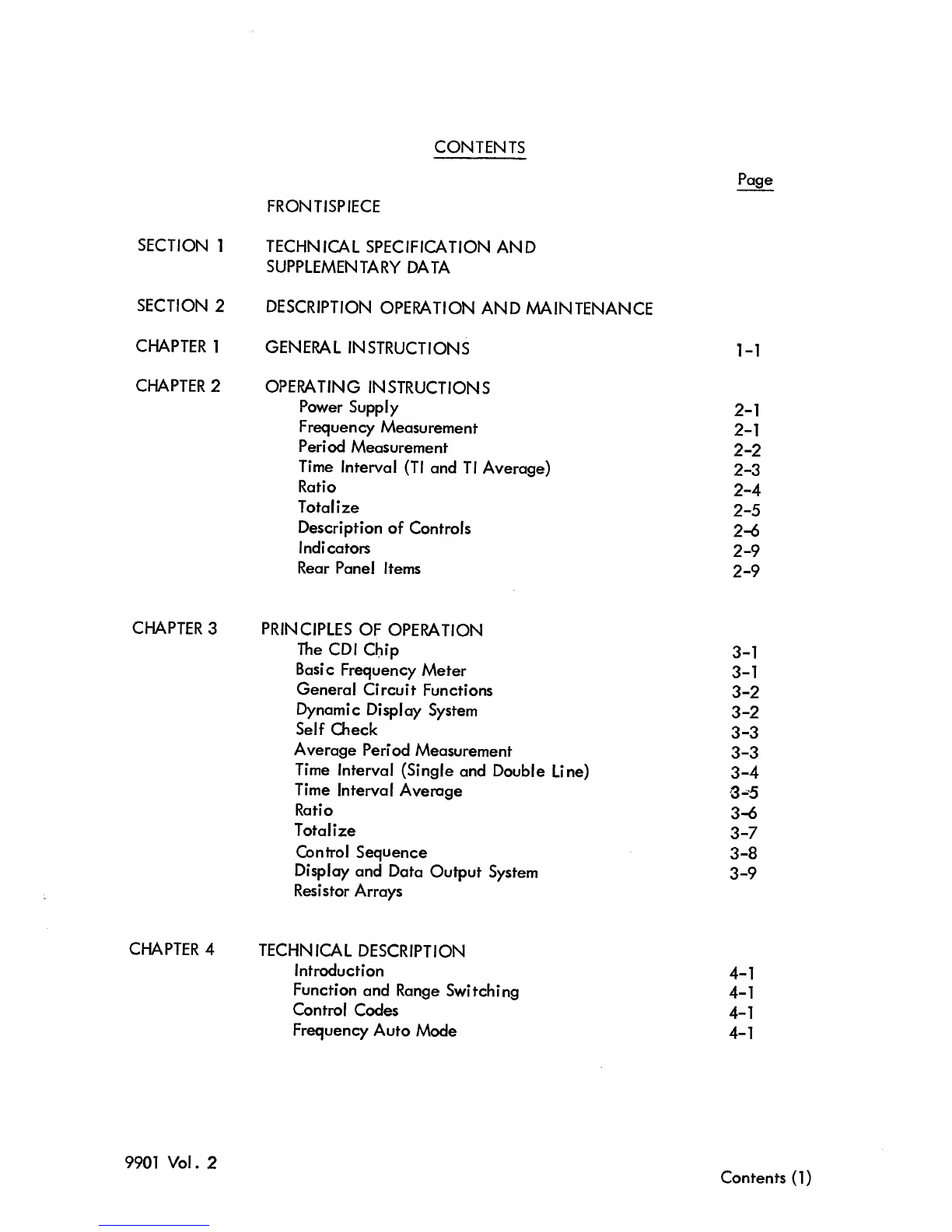
CONTENTS
Page
FRONTISPIECE
SECTION 1TECHNICAL SPECIFICATION AND
SUPPLEMENTARY DATA
SECTION 2DESCRIPTION OPERATION AND MAINTENANCE
CHAPTER 1GENERAL INSTRUCTIONS 1-1
CHAPTER 2OPERATING INSTRUCTIONS
Power Supply 2-1
Frequency Measurement 2-1
Period Measurement 2-2
Time Interval (Tl and Tl Average) 2-3
Ratio 2-4
Totalize 2-5
Description of Controls 2-6
Indicators 2-9
Rear Panel Items 2-9
CHAPTER 3PRINCIPLES OF OPERATION
The CDI Chip 3-1
Basic Frequency Meter 3-1
General Circuit Functions 3-2
Dynamic Display System 3-2
Self Check 3-3
Average Period Measurement 3-3
Time Interval (Single and Double Line) 3-4
Time Interval Average 3-5
Ratio 3-6
Totalize 3-7
Control Sequence 3-8
Display and Data Output System
Resistor Arrays 3-9
CHAPTER 4TECHNICAL DESCRIPTION
Introduction 4-1
Function and Range Switching 4-1
Control Codes 4-1
Frequency Auto Mode 4-1
9901 Vol. 2Contents (1)

CONTENTS (Confinued)
Data Latch/Unlatch. Normal/Hold and Reset
Page
4-3
Channel 'A' Input 4-3
AC Amplifier 4-3
DC Amplifiers 4-4
'B' Channel DC Amplifier 4-4
Bounce Protection 4-4
'A' Channel DC Amplifier 4-5
Check Mode 4-5
Slope Selection 4-5
Manual Start/Stop 4-6
Data Output and Display System 4-6
Multiplex Readout and Display 4-6
Decimal Point and Overflow Decode 4-6
Gate Indicator LP2 4-7
Display Time and Reset Generator 4-7
Display Time Circuit 4-7
Reset Pulse 4-7
Manual Reset 4-8
External Reset 4-8
Segment Check 4-8
Frequency Standard 4-8
Standard Oscillator Assembly 19-0834 4-8
Optional Oscillator 4-8
Frequency Doubler 4-9
1MHz Reference Output 4-9
External Standard Input 4-9
Power Supply 4-9
+5V Stabilization 4-9
-5V Stabilization 4-9
On/Off Switching 4-10
CDI Chip 2V Supply 4-10
CHAPTERS MAINTENANCE
Test Equipment Required 5-1
Removal of Covers 5-2
Transformer Voltage Selection 5-2
Voltage Selection Diagram 5-3
Fuses 5-4
Power Lead 5-4
Power Supply Check 5-4
9901 Vol. Contents (2)

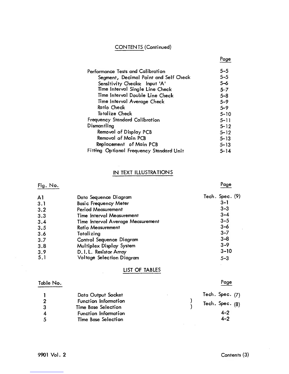
CONTENTS (Conti nued)
Page
Performance Tests and Calibration 5-5
Segment, Decimal Point and Self Check 5-5
Sensitivity Checks: Input 'A' 5-6
Time Interval Single Line Check 5--7
Time Interval Double Line Check 5-8
Time Interval Average Check 5-9
Ratio Check 5-9
Totalize Check 5-10
Frequency Standard Calibration 5-11
Dismantling 5-12
Removal of Display PCB 5-12
Removal of Main PCB 5-13
Replacement of Main PCB 5-13
Fitting Optional Frequency Standard Unit 5-14
Fig. No.
IN TEXT ILLUSTRATIONS
Page
A1 Data Sequence Diagram Tech. Spec.
3.1 Basic Frequency Meter 3-1
3.2 Period Measurement 3-3
3.3 Time Interval Measurement 3-4
3.4 Time Interval Average Measurement 3-5
3.5 Ratio Measurement 3-6
3.6 Totalizing 3-7
3.7 Control Sequence Diagram 3-8
3.8 Multiplex Display System 3-9
3.9 D. I. L. Resistor Array 3-10
5.1 Voltage Selection Diagram 5-3
Table No.
LIST OF TABLES
Page
1Data Output Socket Tech. Spec.
2Function Information
1
Tech .Spec
.
3Time Base Selection
4Function Information 4-2
5Time Base Selection 4-2
9901 Vol. 2Contents (3)
LIST OF TABLES (Continued)
Table No. Page
6Test Equipment Required 5-1
7Self Check Readout 5-5
8Input 'A' Sensitivity Check 5-6
9Time Interval Single Line Check 5-8
SECTION 3PARTS LISTS, COMPONENT LAYOUTS AND CIRCUIT DIAGRAMS
Component Layout; Display Assembly Fig. 1
Parts List 1; Display Assembly
Circuit and Layout: Oscillator PCB Assembly Fig. 2
Parts List 2; c5sci Ilator PCB Assembly
Parts List 3: Chassis, Front and Rear
Panel Assemblies
Parts List 4a and 4b; Main PCB Assembly
Component Layout; Main PCB Assembly Fig. 3
Overall Circuit: 9901 Fig. 4
SECTION 4APPENDICES AND CHANGE INFORMATION
APPENDIX 1: SERIAL TO PARALLEL INTERFACE UNIT
9901 Vol. 2Contents (4)

V.
liSaWWi4i=S£l£ifLSI'JJ£a

DATA FORMAT PRINCIPLES
DATA OUTPUT FORMAT
A4. In standard format the b.c.d. output data Is available at the 28-way edge
connector in abit parallel byte serial form. The data is sequenced by a
10 kHz synchronising signal. The data presentation is delayed 0.5 ps from the negative
edge of the S)^nchronising signal. An additional synchronising pulse (Ro) determines the
first state (10 digit). Accessories are available to give data output in parallel format
(for printers etc.) or lEC/ASCII bus compatible format. (Options)
The ten data output states are as follows: the timing Is shown below.
States Facility
1fo 8Digit (display information).
9Overflow for 10^, 10^, 10^ and 10^ digits on
pins D,E, 4and 5respectively.
10 Decimal point posjTion in kHz units, plus overflow
information for 10^ digit, via pin 5.
II
1100 VS I
II
10 KHz SYNC.
(PIN FI
Ro (PIN 12)
OUTPUT STATES
DATA OUTPUTS
0-5
MS
12
I
10 ^110 ^
5I6I7I89
to 7
10 1
DIGIT DATA
Data Sequence Diagram
OVER OVERFLOW
FLOW AND dp.
Fig A.1
9901 Vol.2 Tech. Spec. (9)

1.GENERAL
II IQt^= J=PJ CJ-FJ CAJJ_QN
Model 9901 is a6digit 50 MHz Ajforanging
Universal Counter Timer.
2. MEASURING FUNCTIONS
Modes of Operation: Frequency (Manual), Frequency (Autoranging),
Single and Multiple Period, Single and Multiple
Ratio, Single and Double Line Time Interval,
Single and Double Line Time Interval Averaging;
Totalizing.
3. DISPLAY
4.
Format:
Latch:
Six digit in-line, LED seven segment display.
Decimal point automatically positioned.
The display is latched for Frequency, Period and
Ratio measurement and automatically unlatched in
all other modes.
Overflow Indicator:
Gate indicator:
Display Time:
A^asurement Check:
Segment Check:
Reset:
LED ill uminated when overflow occurs.
LED ill uminated when gate is open.
Gate time plus 0.25s in Frequency, Period and
Ratio modes.
2.0s in other modes. Aswitched hold position is
provided.
Counter reads 1Mtiz.
Sets display LED's to 8when Check and Reset
selected.
Manual by push-button, or automatic.
CHANNEL AINPUT -A.C. COUPLED
Frequency Range: 10 Hz to 50 MHz.
Sensitivity: lOmVr.m.s.
Maximum Input Level: 250V r.m.s. up to 10 kHz.
50V r.m.s. up to 100 kHz.
lOV r.m.s. above lOO kHz.
400V d.c.
9901 Vol.2 Tech. Spec (1)

5.
Input Impedance: 1Mfi in parallel with approximately 25pF.
CHANNELS A&B-D.C. COUPLED
6.
Frequency Range: DC to 10 MHz,
Sensitivity: ±0.25V about +1V nominal or contact closure
to earth
.
Maximum Input Level:
Pulse Duration:
Input Impedance:
FREQUENCY MEASUREMENT
±35V.
50 ns minimum at trigger points.
Approximately 10 kCi (Falling to IkQ above
approximately +5V).
7.
Input:
Frequency Range:
Coupling:
Channel A.
DC to 50 MHz (direct).
AC or DC
Gate Times: Manual: 1ms to 100s in decade steps.
Automatic: Gate times up to Is are selected
automatically to avoid overspill. Designed hysteresis
avoids undesirable range changing at small frequency
deviations.
SINGLE &MULTIPLE PERIOD MEASUREMENT
Input Channel: Channel A,
Range: 1ps to Is.
Clock Unit: 1ps.
Coupling: AC or DC
Periods Averaged: 5
1to 10 in decade multiples
Accuracy: ±0.3% ±Freq. standard
Number of periods averaged accuracy
(at 50 mV r.m.s. a.c. input with 40 dB S/N i
Bandwidth: Automatically reduced to 10 MHz (3 dB) when
Period selected.
o
9901 Vol.2 Tech. Spec. (2)

8,TIME INTERVAL SINGLE &DOUBLE LINE
9.
Input Channel:
Time Range:
Clock Units:
Single Line: Channel B,
Double Line: Start Channel B: Stop Channel A.
4
100 ns to 10 s(2.8 hours approximately).
100 ns to 10 ms.
Coupling: DC
Start/Stop Signals: Electrical or contact
Manual Start/Stop:
Trigger Slope Selection:
Accuracy:
Bounce Protection:
By single push button on fromt panel.
Electrical. Positive or negative slopes can be
selected on both Start and Stop signals.
Contact .Opening or closure can be selected
on both Start and Stop signals. For trigger
error see page Tech. Spec. (4).
±1count ±trigger error ±frequency standard
accuracy.
A10 ms dead time is automatically Included
when contact operation is selected.
TIME INTERVAL AVERAGING SINGLE &DOUBLE LINE
Input Channel:
Time Range:
Single Line: Channel B.
Double Line: Start Channel B: Stop Channel A.
150 ns to 0.1s
Dead Time between Intervals:
Clock Unit:
Time Intervals Averaged:
Accuracy:
150 ns minimum.
100 ns.
5_
1to 10 in decade multiples.
±Frequency standard accuracy ±system error
±averaging error.
System error: 10 ns per input channel. This is
the difference in delays between start and stop
signals and can be minimised by matching
externally.
9901 Vol.2 Tech .Spec. (3)

Accuracy: (Gsnt'd). Averaging Error: Trigger error +100 ns
y] (Intervals Averaged)
10 .RATIO
One Frequency Input:
Other Frequency Input:
Frequency Range (channel A)
Trigger Error:
(ns) Signal slope at trigger point
(V/ps)
Channel A
Channel B
DC to 50MHz
Frequency Range (channel B) DC to 10 MHz
Accuracy: ±1count ±trigger error on channel B(see
above)
Reads: Frequency Axn
Frequency B
Multiplier n: 1to 10^ in decade multiples
TOTALIZING
Input Channel: Channel A(DC to 10 MHz).
Maximum Rate: 1events per second
.
Pulse Width: 50 ns minimum at trigger points.
Prescaling: Events can be prescaled in decade multiples,
(n) from 1to 10^.
Reads: Number of input events
n
Manual Start/Stop: Single push button on front panel
.
Electrical Start/Stop: By electrical signal applied to Channel B.
Specification as for Time Interval, single line
working
.
FREQUENCY STANDARD See also Option 04A and 04B.
Frequency: 5MHz.
Temperature Stability: ±8parts in 10^, over temperature range 0°C
to +55 C. ±3 parts in 10° over temperature
range +20°C to +40°C.
9901 Vol.2 Tech .Spec. (4)

13 .
Average Ageing Rate: ±1part in 10 per month three months after
delivery but less than ±1part in 10^ in the
first year.
Frequency Standard Output: 1MHz t.t.l. compatible rectangular wave.
EXTERNAL STANDARD
Frequency:
Input Socket:
14. EXTERNAL SIGNALS
Data Outputs:
Other Outputs:
1MHz.
Applied to channel Binput socket and provides
external standard for Frequency and Period
measurement only.
Eight digits with overflow and decimal points in
serial BCD form at standard t.t.l. levels. Refer
to Table 1on page (7).
Function and timebase data. Schmitt trigger outputs
from both channels.
Inputs:
15. POWER REQUIREMENTS
Supply:
Voltage Ranges (a.c.):
Reset and print hold. (Also refer to Option 01).
94V to 265V r.m.s., 45 to 450 Hz a.c.
Eight ranges selected by transformer connection
and link:
94V to 106V
106Vto 119V
118V to 132V
188V to 212V
200V to 225V
212V to 239V
223V to 251V
235V to 265V
Consumption: 20 VA approximately.
16. ENVIRONMENTAL &SAFETY SPECIFICATIONS
Operating Temperature Range: 0°C to+55°C.
Storage Temperature Range:
Humidity:
Mechanical
:
Safety:
-40°C to +70°C.
95%r.h. at+40°C.
In accordance with lEC 68.
Meets IEC 348 (BS4743)
9901 Vol.2 Tech. Spec. (5)

MECHANICAL Height Width Depth
Case 83 mm 240 mm
Overall 110 mm 284 mm 268 mm
Weight 2.6 kg approximately.
18 .OPTION 01 SERIAL TO PARALLEL INTERFACE
Data and Control
Information: 8decades of data in 4line BCD weighted 1248,
3line decimal point position, print command.
print hold, reset, overflow and time-base information.
All logic levels t.t.l. compatible.
For further details refer to the Appendix in Section 4
at the back of the book.
19. OPTION 04A FREQUENCY STANDARD 9442
Frequency: 5MHz.
Ageing Rate: ±3parts in 10 /day after 3months continuous operation.
Warm-up Time: Better than ±2parts in 10^ within 6minutes.
Temperature Better than ±3parts in 10 per Cover the range
Stability: -10°Cto+45C.
20. OPTION 04B FREQUENCY STANDARD 9421
Frequency: 5MHz.
Ageing Rate: ±5parts in 10^^/day after 3months continuous operation.
Warm-up Time: Better than ±1part in 10 within 20 minutes.
Temperature Better than ±6parts in 10^^ per °C over the range
Stability: -10°C to445°C.
21. ACCESSORIES
Accessories Supplied: Operating handbook and spare fuses.
Accessories Available: 19-inch rack mounting kit.
Carrying Case.
9901 Vol.2 Tech. Spec. (6)

Ii-lidIyJMy==QiJA
DATA OUTPUT CONNECTIONS
AT Dafa and command information is provided on a28-way edge connector accessible
via aremovable cover on the rear panel. The facilities and pin connections are
listed in Table 1below. The logic for time base and function data is given in Tables 2and 3.
TABLE 1
Data Output Socket
Pin Facility Pin Facility
1-5V (nominal) AOV
2+5V (nominal) BOverflow (static indication)
3Key Way CKey Way
47(BCD) DT(BCD)
5s' (BCD) E2(BCD)
6External Hold Input F10kHz Sync
.
7External Reset Input HMain Gate
8Auto JNot Used
9cFunction K—N
ZTime Base
10 b*Information L7>Information
11 (See Table 2) MXJ(See Table 3)
12 Ro NNot Used
13 Hold/Reset PSchmitt 'B' 1See
14 Not Used RSchmitt 'A' JNOTE 1
NOTES: 1.Schmitt Aand Schmitt 'B' outputs on pins Rand Pshow the states of
d,c. channel Schmitt triggers.
2. External Hold Input
To extend the cycle time the external hold signal (logic '0') must be applied
during the gate or hold time. To initiate anew measurement cycle the
external hold must go 'high' for not less than 200 ps.
3. External Reset Input
To apply external reset the level at pin 7must go to logic 'O' for not less
than 5ms. On reverting to '1 'level the display resets to 'all zeros' and a
new measurement commences.
9901 Vol.2 Tech. Spec. (7)

FUNCTION AND TIMEBASE LOGIC CODES
FuncHon Data
A2 Function information format: 3lines coded as follows. The table gives the logic
available at the edge connector. The inverse levels are applied to the CDI
Chip in the instrument.
TABLE 2
Function Information
Function Code
abc
Frequency 111
Average Period 011
Totalize A010
n
Ratio A
"T 110
T. 1. (single line or double
not averaged)
line 001
T.l. (single line or double
averaged)
line 101
Time Base Selection Data Output
A3 Time Base information: 3lines coded as follows.
TABLE 3
Time Base Selection
Code
Xyz
Frequency
Gate Time Multiplier
n' Time Interval
Clock
111
011
101
001
110
010
1ms
10 ms
100 ms
1sec
10sec
100 sec
1
^°2
10^
0.1 ps
1ps
10ps
100 ps
1ms
10ms
9901 Vol.2 Tech .Spec .(8)

Table of contents
Other Racal Instruments Cash Counter manuals