Racal Instruments 9081 User manual

The Electronics Group

PUBLICATION NUMBER WOH 7204
ISSUE 10.8.83
AND
SYNTHESIZED
SIGNAL GENERATORS
RACAL-DANA INSTRUMENTS INC.
4Goodyear Street, PO Box C 19541, Irvine, Ca 92713, USA.
Telephone: (714) 859-8999. TWX: 910-595-1136, TLX: 678-341
RACAL-DANA INSTRUMENTS LTD.
Duke Street, Windsor, Berkshire SL4 1SB, United Kingdom
Telephone: Windsor (07535) 68101, TLX: 847013
RACAL-DANA INSTRUMENTS S.A.
18 Avenue Dutartre, 78150 Le Chesnay, France
Telephone: (3) 955-8888, TLX: 697 215
RACAL-DANA INSTRUMENTS GmbH
Hermannstrasse 29, D-6078 Neu Isenburg, Federal Republic of Germany
Telephone: 06102-2861/2, TLX: 412896
RACAL-DANA INSTRUMENTS ITALIA SRL
20161 Milano, Via Angeloni 8, Italy
Telephone: (02) 6459558/6468189 TLX: 315697
PUBLICATION DATE: NOVEMBER 1976
Copyright ©1976 by Racal-Dana Instruments Ltd. Printed in England. All rights reserved.
This book or parts thereof may not be reproduced in any form without written permission of the publishers.


in case of Electric Shock
1. Lay victim on his back.
2. Clear victim’s mouth and throat.
3. Tilt victim’s head back as far as
possible and raise his head.
Have someone else send for aDoctor
Keep patient warm and loosen his clothing
4. Pinch victim’s nostrils.
5. Take adeep breath.
6. Cover the victim’s mouth with yours
and blow, watching his chest rise.
Note: Blow forcefully into adults, but
gently into children.
7. Move your face away to allow victim
to breathe out, watching his chest fall.
8. Repeat first five to ten breaths at a
rapid rate; thereafter, take one breath
every three to five seconds.
9. Keep victim’s head back as far as
possible all the time.

Racal-Dana Instruments August 1983
SYNTHESIZED SIGNAL GENERATOR 9082
The changes listed below have been made on some instruments having serial
numbers above 4010.
Changes found to apply to the instrument with which this manual is to be
used should be incorporated in the manual by manuscript amendment.
PARTS LIST 4
Resistors
Capacitors
20-2103 Delete '86'
20-2223 Delete '87'
Add new components:
'20-2123 Carbon Film 1/4 512 kR87
'20-2332 Carbon Film 1/4 53.3k' R86
'20-1521 Carbon Film 0.1 5Ik Ra'
21-1512 Delete *6A T
Add new component
:
'21-1764 Ceramic 100 2In Ca'
FIG. 9
R86
R87
C64
Amend value to 3.3k
Amend value to 12k
Delete all details
Add new components Ra (Ik)
pins 2and 3of IC5. and Ca (In) in series between
PARTS LIST 3b
Capacitors 21-1677 Add 'Ca'
FI G. 7
Add Ca (5.6p) between IC3 pin 6and 0V.
AR5184
9081/9082
Issue 10
Change No.1

POZIDRIV' SCREWDRIVERS
Metric thread cross-head screws fitted to Racal equipment are of the 'Pozidriv 1
type. Phillips typeand 'Pozidriv' type screwdrivers are not interchangeable,
and the use of the wrong screwdriver will cause damage. POZIDRIV is a
registered trade mark of G.K.N. Screws and Fasteners Limited. The ’Pozidriv 1
screwdrivers are manufactured by Stanley Tools Limited.

lACAlL
modulation
liequnncy ,
frequency MHz
•
•


IMPORTANT NOTES
1.This manual is applicable to Model 9081, 9081 H, 9082 and 9082H
instruments.
2. The most significant differences between the models are:-
(a) The frequency range for Models 9081 and 9081 His 5to 520 MHz
while that for Models 9082 and 9082H is 1.5 to 520 MHz.
(b) The frequency range for external AM is d.c. to 100 kHz for
Models 9081 and 9081H, and d.c. to 20 kHz for Models 9082 and
9082H.
3* Models 908WH and 9082H incorporate amodular r.f. amplifier which
increases the maximum r.f. output to +13 dBm into 50Q. To maintain
the same minimum output level an additional 10 dB step is provided on the
output attentuator.
9081 &9082

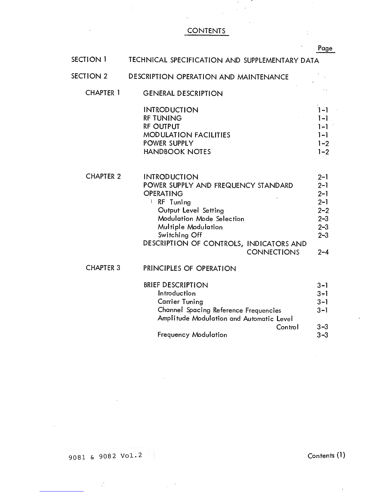
CONTENTS
Page
SECTION 1TECHNICAL SPECIFICATION AND SUPPLEMENTARY DATA
SECTION 2DESCRIPTION OPERATION AND MAINTENANCE
CHAPTERl GENERAL DESCRIPTION
INTRODUCTION 1-1
RF TUNING 1-1
RF OUTPUT 1-1
MODULATION FACILITIES 1-1
POWER SUPPLY 1-2
HANDBOOK NOTES 1-2
CHAPTER 2INTRODUCTION 2-1
POWER SUPPLY AND FREQUENCY STANDARD 2-1
OPERATING 2-1
1RF Tuning 2-1
Output Level Setting 2-2
Modulation Mode Selection 2-3
Multiple Modulation 2-3
Switching Off 2-3
DESCRIPTION OF CONTROLS, INDICATORS AND
CONNECTIONS 2-4
CHAPTER 3PRINCIPLES OF OPERATION
BRIEF DESCRIPTION 3-1
Introduction 3-^1
Carrier Tuning 3-1
Channel Spacing Reference Frequencies 3-1
Amplitude Modulation and Automatic Level
Control 3-3
Frequency Modulation 3-3
9081 &9082 Vol.2 Contents (1)

Page
Phase Modulation (OM) 3-3
Frequency Counter and Display 3“3
Tune (Spin Wheel) Encoder 3-4
CHAPTER 4TECHNICAL DESCRIPTION
INTRODUCTION
LOGIC CIRCUIT SYMBOLS
MAIN OSCILLATOR (VCOl) ASSEMBLY 19-0841 4-1
LOGIC PCB ASSEMBLY 4-2
300kHz Reference Frequency 4-2
Fine Tune Reference 4-2
Tuning (Spin Wheel) Input 4-3
Pul se Multiplier and Up/Down Detector 4-3
Step Switch 4-3
Pulse Divider 4-3
Principles of Channel Spacing Control 4-4
Channel Spacing Control Circuit 4-5
DIVIDER AND PHASE DETECTOR ASSEMBLY 19-0846 4-6
Introduction 4-6
'N' Counter 4-7
Digit Blanking 4-7
HF Divider 4-8
Phase Detector 4-9
Read Only Memory (ROM) 4-10
Half Octave Output 4-11
End Stop Control 4-1
1
OUTPUT SYSTEM ASSEMBLY 19-0843 4-1
1
Introduction 4-11
RF Input 4-1
1
Range Switching 4-11
Range 5Filtering and Half Octave Selection 4-11
Range 4Division and Filtering 4-12
Range 3Division and Filtering 4-12
Range 2Division and Filtering 4-12
Range 1Mixer and Filtering 4-13
RF Output Amplifier 4-13
Output Metering 4-13
Amplitude Modulator Stage 4-13
ALC and Carrier Level Setting 4-13
X2 Output 4-14
AM Audio Input 4-14
9081 &9082 Vol.2 Contents (2)

Page
120 MHz LOOP ASSEMBLY 19-0849 4-15
Introduction 4-15
120MHz Oscillator 4-15
Phase Detector Path and Display Blanking 4-15
300 kHz Reference Output 4-15
Master Reference Inputs 4-16
COUNTER ASSEMBLY 19-0845 4-1
6
INTRODUCTION 4-16
LOGIC VOLTAGE LEVELS 4-16
COUNTER PRINCIPLES 4-17
Reference Frequency 4-17
Time Base and Shift Delay Data 4-17
Multiplex Readout 4-17
Shift Data 4-20
CIRCUIT DESCRIPTION 4-21
Carrier Input 4-21
Range 1Select 4-21
Time Base Drive 4-21
Time Base Encoding and Delay 4-21
Trailing Digit Blanking 4-22
Leading Digit Blanking 4-22
Complete Display Blanking 4-22
AUDIO OSCILLATOR ASSEMBLY 19-0847 4-23
Introduction 4-23
Audio Oscillator Circuit 4-23
FM LOOP ASSEMBLY 19-0844 4-24
Principles of the System 4-24
Circuit Description: 400kHz Loop 4-24
Sweep Circuit 4-26
Deviation Monitoring 4-27
Modulation Audio for FM 4-28
Phase Modulation ((^M) 4-2 8
FM Switching 4-28
POWER SUPPLY 4-30
9081 &9082 Vol.2 Contents (3)

CHAPTER 5MAINTENANCE Page
POWER SUPPLY (MAINS) VOLTAGE SELECTION 5-1
REMOVAL OF COVERS 5-3
POWER SUPPLY TESTS 5-3
TUNING CHECKS 5-5
PRELIMINARY SYSTEM CHECKS 5-8
Output System 5-8
FM System 5-9
CALIBRATION 5-10
OUTPUT SYSTEM ASSEMBLY 5-10
AUDIO OSCILLATOR ASSEMBLY 19-0847 5-13
FM LOOP ASSEMBLY 5-14
DISTORTION CHECK 5-15
LEVEL ACCURACY CHECK 5-17
SPURIOUS CHECK 5-18
FAR-OFF AND CLOSE-IN NOISE CHECKS 5-19
RESIDUAL FM CHECK 5-20
FM DEVIATION CHECK 5-21
FM DISTORTION CHECK 5-23
PHASE MODULATION CHECK 5-23
AM DEPTH AND DISTORTION CHECK 5-24
FM FREQUENCY RESPONSE CHECK 5-26
AM FREQUENCY RESPONSE CHECK 5-27
RECONNECTION OF HIGH LEVEL AMPLIFIER 5-28
LEVEL ACCURACY CHECK 5-28
DISTORTION CHECK 5-29
AM DEPTH AND DISTORTION CHECK 5-29
ATTENUATOR CHECK 5-29
INTERNAL STANDARD OUTPUT CHECK 5-30
INTERNAL FREQUENCY STANDARD CALIBRATION 5-30
INTERNAL REVERSE POWER PROTECTION UNIT OPTION 5-31
LIST OF TABLES
Table
1Frequency Increments in Z\f Mode 2-6
2Channel Spacing Control 4-5
3Counter Assembly Data 4-20
4Mains Voltage Selection Switches 5-1
5List of Test Equipment Required 5-2
6Mains Input Resistance Readings 5-4
7Carrier Frequency Ranges 5-7
8Channel Spacing Check 5-7
9Distortion Check 5-16
9081 &9082 Vol.2 Contents (4)

Table Page
10 Residual FM Check 5-21
11 FM Deviation Check 5-22
12 Phase Modulation Check 5-24
13 AM Depth and Distortion Check 5-25
14 FM Frequency Response Check 5-26
15 AM Frequency Response Check
IN TEXT ILLUSTRATIONS
5-27
Fig. No.
2.
1
9082 Front Panel 2-5
3.1 Simplified Block Diagram 3-2
3.2 Theoretical Block Diagram 3-5
4.1 Functional Block Diagram: Counter Assembly 4-18
4.2 Multiplex Display System 4-19
4.3 Functional Block Diagram: FM Loop Assembly 4-25
4.4 Phase Modulation Principle 4-28
5.1 Tag Strip Test Points 5-5
5.2 TP3 Waveform 5-14
SECTION 3PARTS LISTS, COMPONENT LAYOUTS AND
CIRCUIT DIAGRAMS
Chassis Layout: Topside View Fig. 1
Chassis Layout: Underside View Fig. 2
Parts List 1:Main Oscillator Assembly 19-0841
Component Layout) Main Oscillator Assembly 19-0841 Fig.
3
Circuit )
Parts List 2: Logic Assembly 19-0842 and 19-0948
Component Layout: Logic Assembly 19-0842 &19-0948 Fig. 4
Circuit: Logic Assembly 19-0842 anc^19-0948 Fig. 5
Parts List 3: Output System Assembly 19-0843 and 19-0949
Component Layout: Output System Assembly 19-0843 Fig. 6
Circuit: Output System Assembly 19-0843 and 19-0949 Fig. 7
Parts List 4: FM Loop Assembly 19-0844
Component Layout: FM Loop Assembly 19-0844 Fig. 8
Circuit: FM Loop Assembly 19-0844 Fig. 9
Parts List 4a: FM Mute Assembly 19-0953
Circuit and Interconnections: FM Mute Assembly 19-0953 Fig. 9a
9081 &9082 Vol.2 Contents (5)

Parts List 5: Counter Assembly 19-0845
Component Layout: Counter Assembly 19-0845 Fig. 10
Circuit: Counter Assembly 19-0845 Fig. 11
Parts List 6: Divider &Phase Detector Assembly 19-0846
and 19-0950
Component Layout: Divider &Phase Detector Assembly 19-0846
and 19-0950 Fig. 12
Circuit: Di vider &Phase Detector Assembly 19-0846
and 19-0950 Fig. 13
Parts List 7: Audio Oscillator Assembly 19-0847
Component Layout: Audio Oscillator Assembly 19-0847 Fig. 14
Circuit: Audio Oscillator Assembly 19-0847 Fig. 15
Parts List 8: Display Assembly 19-0848
Component Layout:)
Circuit: )
Display Assembly 19-0848 Fig. 16
Parts List 9: 120MHz Loop Assembly 19-0849
Component Layout: 120MHz Loop Assembly 19-0849 Fig. 17
Circuit: 120MHz Loop Assembly 19-0849 Fig. 18
Parts List 10: Power Supply Fig. 19
Circuit: Power Supply
Parts List 11: Front Panel Components
Circuit: Front Panel Switching Diagram Fig. 20
Component Location: Front Panel Assembly Fig. 21
Parts List 12: Miscellaneous
Overall Block Diagram Fig. 22
SECTION 4APPENDICES AND CHANGE INFORMATION
9081 &9082 Vol .2 Contents (6)

SECTION 1
T_E_C HNJ CAL_S PEC 1FIQAILQK

RF CHARACTERISTICS
11g±IN LQ Aj_=JfJJJfl cAJjjiy
Frequency Range:
Channel Spacing (kHz):
(Step Size)
Frequency Indication:
Accuracy of Frequency
Indication:
1.5 MHz (5 MHz for 9081) to 520 MHz in five
bands :-
Band 1 1 .5 MHz (5 MHz for 9081) to 35 MHz
Band 231 MHz to 67 MHz
Band 361 MHz to 134 MHz
Band 4122 MHz to 268 MHz
Band 5244 MHz to 520 MHz
Ten channel spacings are provided, and these are
grouped to serve different national requirements
as follows:-
(1) 5, 10 and 20 kHz.
(2) 6.25, 12.5, 25 and 50 kHz.
(3) 15, 30 and 60 kHz.
The frequency increments in Afmode are
given in Chapter 2, page 2—6
.
The output frequency is continuously measured
and displayed on an 8-digit LED display. The
resolution is 100 kHz in FAST TUNE, 1kHz in
SLOW TUNE and 10 Hz in HOLD.
+1count +frequency standard accuracy.
Frequency Stability: (1) FINE TUNE off:- the step frequencies are
phase-locked to the internal frequency
standard
.
(2) FINE TUNE on:-
(a) Band 1:less than 100 Hz change per
10 minutes after 30 minutes.
(b) Bands 2to 5: less than 1ppm change
per 10 minutes after 30 minutes.
9081 &9082 Vol .2Tech .Spec. (1 )
.

FREQUENCY STANDARD
Type:
Frequency:
Ageing Rate:
Warm-Up Time:
Temperature Stability:
Alternative Standard:
External Frequency Standard
Input:
Racal-Dana Type 9442:-
5MHz.
9
+3parts in 10 per day after 3months
continuous operation.
Better than +2part in 10^ within 6minutes from
cold
.
Better than +3parts in 10^ per °C over the
range -10°C to +45°C.
See Optional Accessories.
Frequency:
Minimum Level
:
Maximum Level:
Input Impedance:
SPECTRAL PURITY
Harmonics:
Sub-Harmonically Related
Signals:
Discrete Spurious:
1MHz.
100 mV r.m.s.
10V r.m.s., 100V d.c.
Approximately 1kQ (a.c. coupled).
At least 30 dB below carrier for frequencies
between 5and 520 MHz.
At least 20 dB below carrier for frequencies
between 1.5 and 5MHz (9082 only).
More than 40 dB below carrier: typically
55 dB below carrier.
Bands 2-5:- At least -70 dB at 20 kHz or more
off carrier.
Band 1At least -70 dB at 20 kHz or more off
carrier in the frequency range 5to 120 MHz for
carrier frequencies from 5-35 MHz.
At least -50 dB at 20 kHz or more off carrier for
carrier frequencies from 1.5 to 5MHz (9082 only).
9081 &9082 Vol .2Tech. Spec. (2)
.

Residual FM on CW: Less than 50Hz r.m.s. deviation in 300Hz
to 3kHz bandwidth.
AM on FM: 1% for deviations of 100kHz and less.
Carrier Leakage: The e.m.f. induced in a2-turn 25mm diameter
loop 25mm away from any surface is signifi-
cantly less than IpV into areceiver 5QQ input.
SSB Phase Noise: Better than -105dB/Hz at 20kHz removed from
carrier.
RF OUTPUT
Output Level: (1) The maximum output level is
+3dBm (+13dBm for models 908 1H
and 9082H) into 5QQ. The
minimum output level is -130 dBm
into 5QQ (71nV).
(2) The stepped output level switch provides
attenuation from OdB to 120dB (130dB
for models 908 1H and 9082H) in 1OdB
steps. The switch is calibrated in
dBm into 5CD and in voltage units.
(3) The Vernier control provides continuous
output level variation from —1OdB
to +3dB relative to the output level
switch setting.
Attenuator Accuracy: ±0.1dB per 1OdB step (cumulative with
reference to OdB) ±0.2dB.
Output Level Flatness: (1) Within ±0.7dB relative to 50MHz level
over frequency range 5to 520MHz.
(2) Within ±2.5dB relative to 50MHz level
over frequency range 1.5 to 5MHz
(9082 only).
9081 and 9082 Vol .2Tech. Spec. (3)

Output Level Accuracy: As indicated on the meter to the following
tolerances with attenuator (OUTPUT LEVEL)
controls in 'straight through 1condition and
OUTPUT switch in NORMAL position:-
(1) For carrier frequencies from 5to 520MHz
±0.8dB at +25°
C
±5°
C
±1 .5dB at 0°C and +55°C
(2) For carrier frequnecies from 1.5 to 5MHz
(9082 only)
±3.3dB at +25°C ±5°C
±4dB at 0°C and +55°
C
When Reverse Power Protection Unit 11-1405 or
11-1390 is fitted add ±0.7dB to the above figures.
5QQ Type 'N' connector.
Ratio 1.1to 1(1 .2 to 1if the Reverse Power-Protect
Unit is fitted) with not less than lOdB attenuation
selected.
The output withstands reversed r.f. inputs up
to 1W. Aprotection unit giving protection up
to 50W is available as an optional extra.
The front panel meter is calibrated in dBm
into 5QQ and in volts.
Output Impedance:
Output VSWR:
Output Protection:
Output Meter:
FREQUENCY MODULATION
Frequency Ranges:
Distortion:
(1) Using the internal oscillators: 400Hz,
1kHz and 5kHz.
(2) Using an external source: 20Hz to 100kHz
(±3dB).
Less than 5% at maximum deviations using
internal oscillator.
Deviation Ranges and Modulating External Modulation frequency response: 1
Frequency Ranges: within 3dB from 20Hz to 100kHz for
all ranges.
9081 and 9082 Vol .2Tech. Spec. (4)
This manual suits for next models
1
Table of contents
Other Racal Instruments Inverter manuals
Popular Inverter manuals by other brands

Chicago Electric
Chicago Electric 92708 Assembly and operating instructions

Daikin
Daikin ERX125A7W1B installation manual

Mitsubishi Electric
Mitsubishi Electric FR-D700 Series instruction manual

Gasolarxy
Gasolarxy PG-KITS100W-19.8VS How to use

Kostal
Kostal PLENTICORE plus operating manual

Falco Systems
Falco Systems WMA-IB-HS user manual