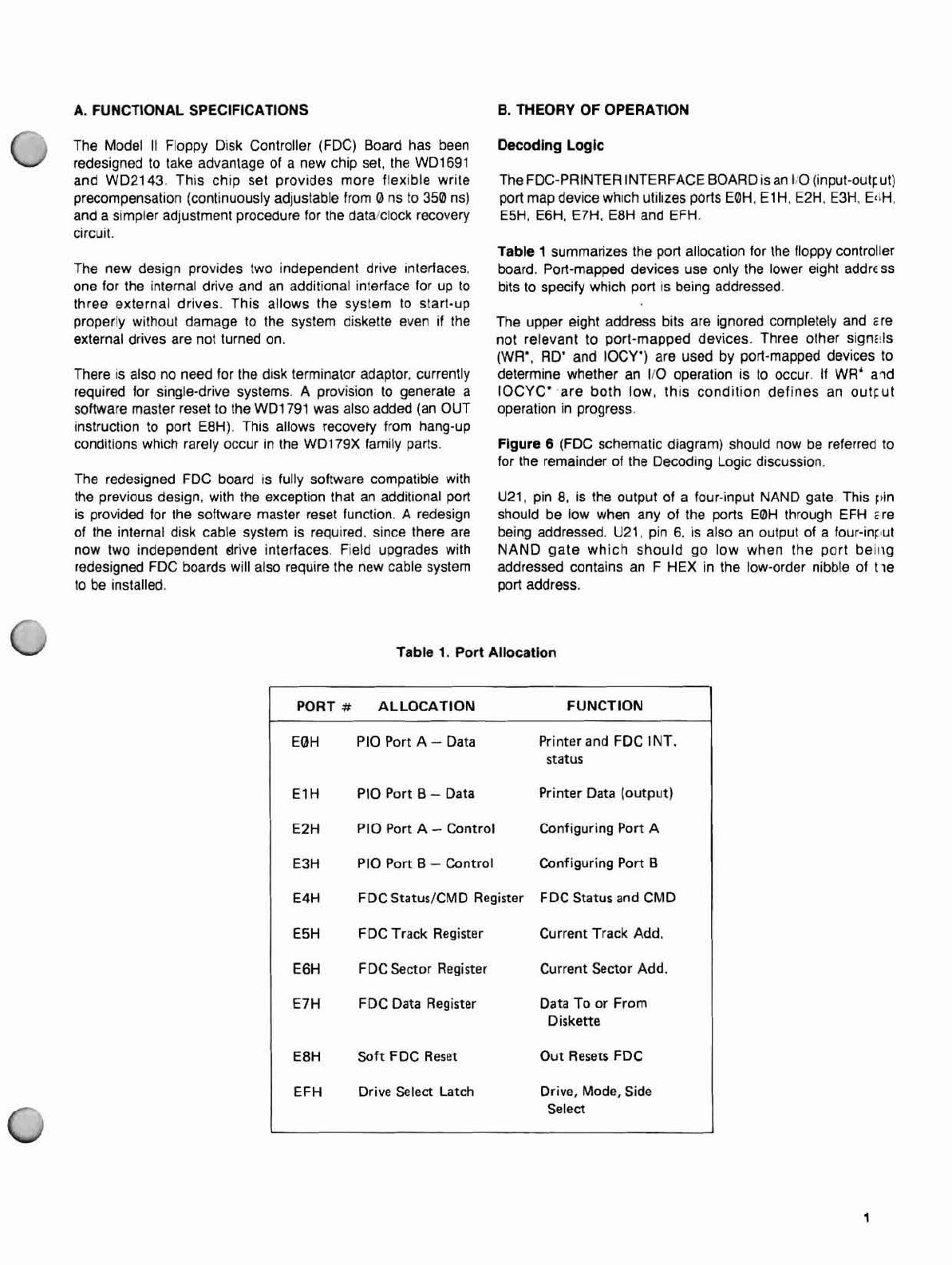
One
110
line is conligured as an oulput and provides the
"prime" signal lor
the
printer interface. The bit allocations
for
this port are detailed
in
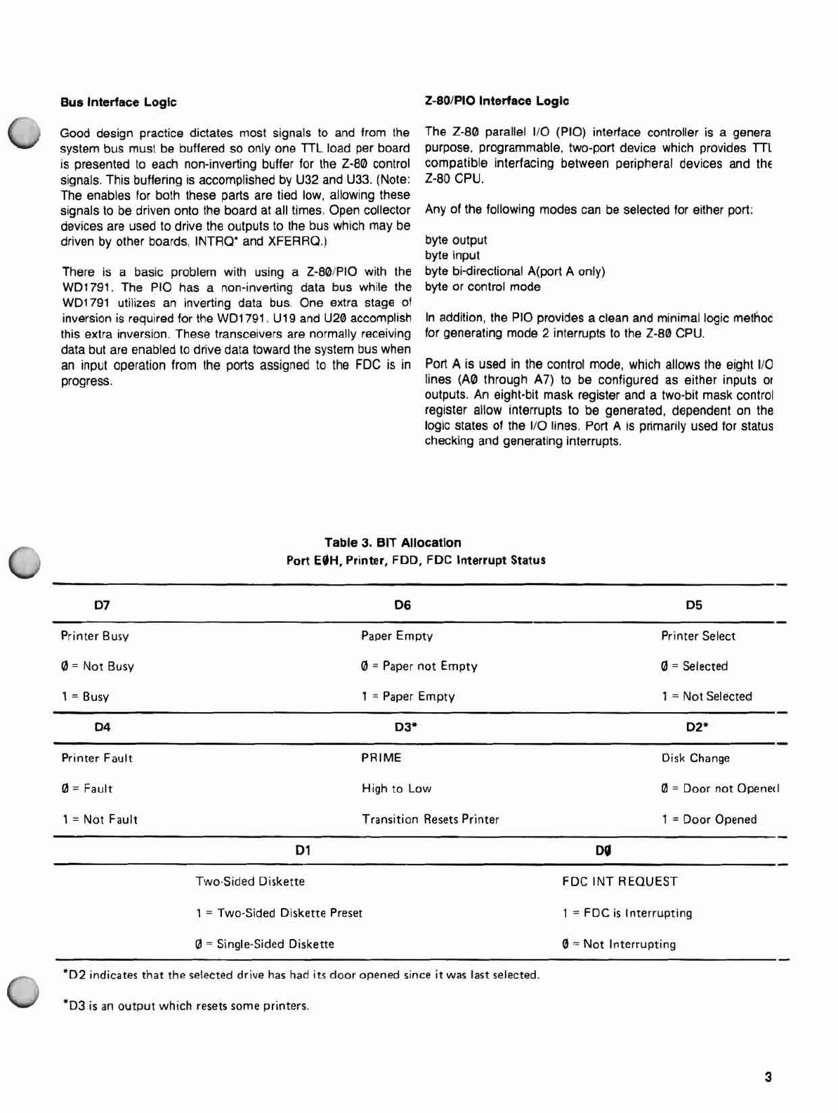
Table
3.
POO
Bis used
in
Ihe output mode lor the purpose
01
outpulling
characters
to
the printer. Tha outputs
01
port B
(BO
through B7)
are isolated lrom
the
printer with
an
octal noninverting buffer,
U4. (Note: The anables
are
tled low, 9atin9 whatever data is
presented
ta
the inputs
01
U4
directly
ta
its outputs.
The
printer
cable system roules this parallel data
ta
the printer,)
Pin
21
of the PlO (U12), labeted BRDV, produces ahigh·
going pulse which indicates valid data is present
on
tha
port B
outputs. The rising edge
olthis
pulse provides atrigger for pin
3of
U6.
U6
is aone-shot which produces 1.5
....
5low-going
pulse
at
pin 4when triggered.
The rising edge
01
the 1.5
....
sstrobe is used
by
the
printer
ta
latch Ihe eight bits
of
parallel data present
atthe
outputs
01
U4.
The BRDY signal stays active until Ihe rising edge
01
PACK'
(which indicates
the
printer has accepted Ihe data).
The
rising
edge may also generale an interrupt
il
port Bhas been
programmed
la
use interrupls. This provides
an
eflicienl
method
for
~etermining
when the printer can accept anew
charactar withoui using
status·chec~ing
loops.
The
PlO interfaces direclly la the system
bus
with a'minimum
of external componenls.
00
through
07
(U12) form abi-
directional data path
to
the
syslem bus.
The
signais labeled
AQlI
and
A
11
deterrnine which port is addressed
and
whether
the
data transfer is intended lor the command register.
Il CEPIO·, 10AOI·.
and
ROI'
are
alllow,
an
input operation is
in
progress. If CEPIO· and IOROI·
are
low with ROI· high,
an
output operation is
in
progresS. Il
IEIN
is high.
and
INTROI·,
SVNCI', IOROI' and IEO are low,
an
interrupt
ac~nowledge
cycle for the PlO
15
in
progress. Il SYNCI' is high
and
RESTI'
is
low,
a
Iow
is produced
at
pin 8
01
U14.
Il this sequence
occurs withoul ROI' and IOROI·
low,
the PlO Iogic enters a
reset state.
For
a
more
detalled
discussion of the PlO
operation, consullthe Zilog Z-8fIJIP/O TechnicaJ Manua/.
Dlak
Bu
••
Selector
loglc
The Model
Il
Floppy Disk-Printer Interface Board supports
up
10
lour drives (one internai, three eXlernal). This function is
implemented
by
using Iwo disk-drive interface busses,
one
for
the internai drive and one lor Ihe externat drives. J0
is
the
connector used
lor
the inlernal drive and
P1
is the edge
connector
usecl
for the external drives.
4
U17 and U16 (quad IWo-ta-one data selectors)
are
used
ta
select which set of inpuls
from
the disk drive busses
are
rou:ed
ta
the
1791
FOC
chip,
Pin 1
01
bath parts are
the
control pins
lor the data seleclor.
11
U17, pin 1
and
U
16,
pin 1are high,
lhe
external inputs
are
selected. Alow selects
the
internaI inpu'
s.
This control signal (Iabeled INT'IEXTl
Is
derived Irom
he
outputs of adeclmal decoder (U36). U36 uses Ihe Iower
hur
bits
ollhe
drive·select latch
(U
11)
as its inputs
to
decocle which
drive is selected. The decoder used
in
lhis way prevents
mo}re
than
one
drive Irom being selected al atime.
ReedlWrlte Data Pulse Shaplng
Loglc
Two one-shots
(112
01
U15
and
1/2 al U6) are used
to
enslJre
the
read
and
wrile dala pulses are approximately 250
ns
in
duration
DI.k
Buas Output
Driver.
U25
and
U1
QI
are high-current open collector drivers
use<!
10
bulter
the
oulput signais lrom the drive select latch
and
Ihe
FOC
chip
ta
the
1I0ppy
dis~
drives. (Schematic note: Ecch
output signal ta the drives has Iwo bullers associated
~
iÎh
each signal -one
set
is used lor :he internai drive buss
and
the
other set is used lor the external drive buss.
No
selectlo}ic
is required for Ihese output signaIs since the drive select
toits
define which drive is active.)
Wrlte Precompensatlon and Clock Recovery Loglc
U28 (WD1691), U29 (W02143) and
U24
(lS629), along witt! a
lew passive eomponents, comprise the write precompensatiOfl
and read clock recovery lagic.
The W01691 is an
lSI
device which minimizes
the
extemal
laglc required ta inlerface the
1791
FOC
chip
ta
adisk dri,'e.
With ltle use al
an
external VCO (U24),
the
WD1691
will derive
the
RClK
signal lor the 1791, while providing
an
adjustmllnt
signal for the
VCQ,
to keep
the
RClK
synchronous with t'le
read data Irom the drive.
Write precompensation control signais are also provlded
by
lne
W01691 la Inlerface directly
10
the W02143
(U29)
clcc~
generalor.
The read clock recovery section
01
the
WD1691
has live
n-
puts:
OOEN,
VCQ,
RoO·,
WG
and VFOE·;
and
three
oulpUlS:
PU,
PO·
and
RClK.
The inputs VFOE" and
WG,
when
be,lh
low,
enable the clock recovery
lagie.
When
WG
is
high, awrrle
operation is
in
progress
and
the dock recovery circuits cre
disabled regardless
01
the stale
01
any
other inputs.
The
wrile
precompensalion section
01
the WD1691
W1S
deslgned ta
he
used wilh
the
WD2143
cloc~
generator. Wrte
precompensalion
is
not used
in
single-density mode
and
tle
signal
DOEN
when high indicates Ihis condition,