RCA AR-88.LF User manual

GENERAL PURPOSE
COMMUNICATIONS RECEIVER
MODEL AR-88.LF
INSTRUCTIONS
Manufactured by
RCA Victor Company, Limited
Montreal. Canada

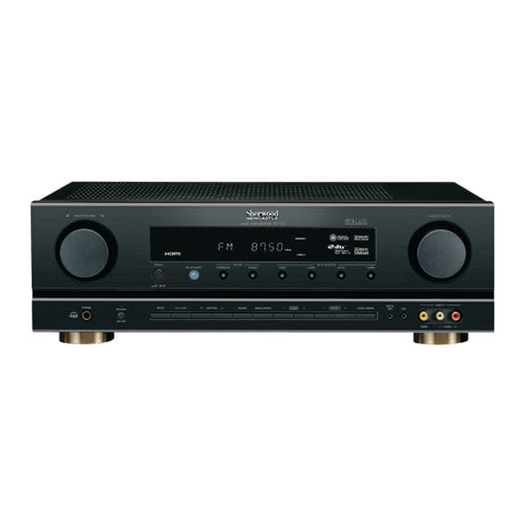
Figure 1.—General Purpose Communication Receiver—Front View.
Figure 2.—General Purpose Communications Receiver—Loudspeaker.
121

TABLE OF CONTENTS
Page
1.
General
4
2.
Technical Details
4
3.
Performance
6
4.
Installation
7
5.
Operation
8
6.
Maintenance.
9
7.
Vibrator Power Supply Unit (MI.22215)
15
TABLES
Table No. I---Performance Data
6
Table No. II--Valve Socket Voltages
9
Table No. III (a)
I.F. Alignment Connections
10
III (b)—I.F. Alignment Adjustments
10
Table No. IV (a)
R.F. Alignment Connections
12
IV (b)--R.F. Alignment Adjustments
13
Table No. V--Parts List, General Purpose Communications Receiver
17
Table No. VI--Parts List, Vibrator Power Supply Unit
21
ILLUSTRATIONS
Figure 1
General Purpose Communications Receiver----Front View
2
2—
CC
C6
44
46
- -Loudspeaker ..
2
3—
46
46
CC
LC
Rear Apron .......
.
7
4—
QC
44
CC
C6
Alignment Layout .
12
5—
-Vibrator Power Supply Unit
MI-^2215 Schematic Diagram
16
6--General Purpose Communications Receiver
Rear View .
23
7—
44
‘6
46
4,
Top View
23
8
„
Top View
Covers Removed
25
*
9--
6'
Bottom View
Covers Removed . 27
*
10
44
---R.F. Unit .
...... . ..
29
*
11
4,
,,
- -ScheMade Diagram
31
12—
,
CC
44
--Selectivity Characteristics
33
13—
"
"
"
Fidelity Characteristics
34
14
„
66
Overload A.V.C. Characteristics
35
*These illustrations are folded in.
ERRATA
Page 6 Paragraph 2.14 MI should read 22215. Page 7 paragraph 4.2 MI should read 22215.
Page 12 Figure 4 C-96.0-97.C-98 Electrolytic condenser should read Oil Filled.
Page 18 Table No. V C-96.0-97.C-98 Dry Electrolytic should read Oil Filled.
{3}

1.2 The
into
(a)
(h)
(c)
(d)
(e)
(f)
GENERAL PURPOSE COMMUNICATIONS RECEIVER
INSTRUCTIONS
1. GENERAL
1.1 This receiver has been designed for general pur-
pose communication. It is designed to withstand
severe climatic and line voltage variations
without appreciable impairment in performance.
following features have been incorporated
the design of this unit.
Mechanical Band Spread, with Single Con-
trol for ease of tuning a previously logged
station.
Automatic Noise Limiter which automa-
tically limits interference to a percentage of
modulation.
Noise Limiter Switch for switching Noise
Limiter on or off.
Continuously variable High Frequency
Tone Control.
Panel Antenna Trimmer for circuit align-
ment.
Variable selectivity, with expansion of the
normal selectivity characteristic for stand-
by, and a crystal filter for ultra sharp selec-
tivity when required. The crystal filter circuit
is adjusted at the factory to give selectivity
characteristics as shown in Figure 12.
Temperature compensated oscillator circuits
on all bands.
Regulation of the anode voltage of the
oscillator, giving good oscillator stability
through normal' variations in line voltage.
Four-ganged Condenser giving high image
ratio, and very low oscillator radiation on
all bands.
Special screening devices have been built
around the gang condenser, the master oscil-
2. TECHNICAL
lator section, and the r.f. amplifier section in
order to minimize oscillator radiation on all
bands.
(k) Tuning lock for service under extreme con-
ditions of vibration.
Frequency Range:—
Band 1
73 to 205 KC
Band 2
195 to 550 KC
Band 3
1480 to 4400 KC
Band 4
4250 to 12150 KC
Band 5
11900 to 19500 KC
Band 6
19000 to 30500 KC
Sensitivity:
Better than 15 microvolts for 20 db
signal to noise ratio, for MCW (A•2)
reception and better than 5 microvolts for
CW (A-1) reception (see table No. 1).
Radiation:—Less than 40 micro-microwatts of
power radiated, as dissipated in resistance con•
nected from Antenna input terminal to ground.
Value of resistance is such as to cause maximum
power to be radiated (see Section 3 below).
Output Power:—(Maximum undistorted)
2.5
Watts when loudspeaker used. When low im-
pedance headphones are used, maximum output
fed to the phones is 100 milliwatts approximate-
ly.
Power Supply Requirements:
115 or 230
volts, 2
5
/
6
0 cycle, 100 Watts or 6 volts D.C.,
12 amps when external power supply MI.22215
is used. (Note—external power supply MI.22215
is only supplied when specially ordered.)
Output Load:— This receiver has provision in
the output circuit to take loads of 2.5 ohms, 20
ohms, and also low impedance headphones.
Mechanical Specifications:—Overall Dimensions
—191 inches wide x 11 inches high x 194 inches
deep. Weight -- 100 Pounds (unpacked).
DETAILS
(see Section 4.4) with a conventional lead-in
wire. The first tuned circuit is provided with a
trimmer condenser adjustable from the front
panel. This insures the proper tuning of this
circuit with any antenna system.
For all bands, conventional antenna and ground
connections may also be used.
The antenna terminal board is provided with
three terminals (see Figures 3 and 7), two of
which may be joined together with a link. When
a single wire antenna is used, the link should he
closed and the antenna connected to "A". If a
ground is used, it should be connected to "G".
1.3
1.4
1.5
1.6
1.7
1.8
1.9
2.1 Circuit Details and Features:—The schematic
diagram of this receiver is shown in Figure 11.
It consists of two stages of R.F. amplification,
first detector, first heterodyne oscillator; three
of I.F. amplification, second detector and
A.V.C., noise limiter, second heterodyne oscil-
lator; A.F. amplifier stage, output power stage,
and power supply system.
2.2 Input Coupling:—The antenna coupling system
is designed to provide optimum coupling from
a 200 ohm transmission line, but equivalent per-
formance is realized with a straight line antenna
[41

If a transmission line or balanced input is used,
the link should be opened and the line con-
nected to terminal "A" and the center terminal.
Protection against damage due to high voltages
across the antenna coil primaries is provided by
a gas gap protector (Type 991 Valve). This
protector will break down with an applied
potential of approximately 50 Volts R.M.S.
2.3 R.F. Amplifier:--The
R-F Amplifier is designed
to provide ample selectivity ahead of the first
detector for minimizing cross modulation and
blocking effects from strong interfering signals
and for obtaining a high degree of image signal
suppression. The amplification is adjusted to
provide optimum signal-to-noise ratio by making
noise contributions of circuits following the first
valve negligible in comparison with the noise
contributed by the first R-F grid circuit; that is,
each tuned circuit in the receiver contributes
some noise voltage, but by making the gain of
the first valve as high _as practicable, the noise
contributed by succeeding circuits is unimportant.
2.4 Band Spread:--The
mechanical band spread
with single control knob enables the operator to
tune quickly to a previously logged station. The
log scale on the main dial and the separate ver-
nier dial provide for exact logging and tuning.
2.5 First Heterodyne Oscillator:
The first hetero-
dyne oscillator is aligned to track with the R-F
Amplifier at 735 kc higher than the signal fre-
quency, thus producing a 735 kc intermediate
frequency in the first detector plate circuit
which is amplified further in the I-F stages. The
oscillator voltage is regulated by the Type VR-
150 regulator valve to provide maximum fre-
quency stability under conditions of variations
in power supply voltage.
2.6 Intermediate Frequency Crystal Filter:
The first
detector plate circuit is tuned to the intermediate
frequency and a balanced link circuit is used to
couple the first detector plate and first I-F grid
circuits. A 735 kc crystal is connected in one
arm of the link circuit by the selectivity switch
and a neutralizing capacitor is connected in the
other. The impendance of the coils in the link
circuit are designed so that the crystal selectivity
characteristic is not impractically sharp. The band
width at two times resonant input may be ad-
justed to 550 cycles, 2000 cycles, 4,000 cycles,
8000 cycles, or 16,000 cycles. For this adjustment
see "Operation".
2.7
Intermediate Frequency Amplifier: —
Three
stages of I-F amplification are used; Type 6SG7
valves are used in all stages and a Type 6H6
valve is used for AVC and second detector.
The first I-F transformer has its primary and
secondary tuned, and is coupled through the
crystal filter link. The second and third I-F
transformers are composed of four tuned cir-
cuits each. These circuits are varied in coupling
by the selectivity switch. The fourth I-F Trans-
former has two tuned circuits.
The third I-F stage is not connected to the
AVC nor to the manual volume control so that
a good AVC characteristic with little overload
distortion is obtained. This also permits the CW
oscillator to be coupled to the grid circuit of
this stage,
2.8 Second Heterodyne Oscillator: —
The second
heterodyne (CW) oscillator is a triode Type
6J5 valve which is electrostatically coupled to
the final I-F stage. A panel control is provided
by means of which the frequency of the hetero-
dyne oscillator and resultant audio beat note
may be varied.
Particular care has been taken in the design of
harmonics.
2.9
Automatic Volume Control:- -The
AVC voltage
is obtained from the second detector, a Type
6H6 valve. A variable delay is obtained depend-
ing on the setting of the R-F gain control.
The second heterodyne (CW) oscillator ex-
citation voltage is just lower than the AVC
diode bias voltage so that it does not decrease
the sensitivity of the receiver.
2.10 Manual Volume Control:—Two
manual vol-
ume controls are provided: an audio gain con-
trol which is employed when the AVC is in
use, to obtain the desired output level, and an
R-F gain control.
2.11 Noise Limiter:—The
noise limiter circuit utilizes
a Type 6H6 valve and limits the noise inter-
ference to 100% modulation and to continuously
lower percentages down to any modulation
whatsoever, determined by the setting of the
noise limiter control.
A noise limiter switch in conjunction with AVC
provides for use of the noise limiter on CW or
on modulated reception when interference is
present.
2.12 Output Valve: —
The Type 6V6GT/G output
valve is resistance coupled from the A-F ampli-
fier, a Type 6SJ7 valve, and operates into an
output transformer which has taps for matching
into a 2.5 ohm load, or headphones. Terminals
are provided on the rear apron for each of these
load impedances. The output from the 2.5 ohm
tap is fed directly to the 2.5 ohm output ter-
minal, while the output from the 20 ohm tap is
fed to the 20 ohm output terminal and also to
a
jack mounted on the panel. With the phone
plug inserted into the jack, the phones are
across the 20 ohm output and a load resistor,
R-56, provides correct matching for the valve
and reduces output supplied to the headphones.
the circuit
minimize oscillator
constants to
[51

//5
V
t. V
/5470
,
2.5
0,.„.„.5
0 ®
01/74/./7
Az
e
a
4
® G
(1400 Az)
O
;
•
/
99/
7B. /
\ ANT- GNO
TER/1 BD.
3.3 Oscillator Stability:—
(a)
Oscillator frequency stable within 0.001%
for line voltage variation of ±
5%.
(b)
Oscillator frequency stable within 0.003%
for temperature change of 1°C.
(c)
Oscillator frequency stable within 0.001%
for total variation of both the audio and
R.F. gain controls.
(d)
Resetting of range switch from either direc-
tion does not vary the frequency of the
oscillator on any band more than 1 kc.
3.4 Dial Resetability
better than 2 kc. when the dial
is reset from either direction, at any frequency.
3.5 Dial Calibration:—Calibration of the dial is accu-
rate to within 0.5%.
3.6 AVC Characteristics:
The AVC circuit holds
the audio output level to 15 db when the MCW
(A-2) input is varied between 10 and 100,000
microvolts at any frequency, with any modula-
tion percentage from 10 to 90, and with any
modulation frequency from 300 to 4000 cycles.
(See Figure 14.)
4. INSTALLATION
4.1 Power Supply:—The power supply circuit is
integral with the receiver. Determine line volt-
age and frequency and check with the rating of
the receiver. The power transformer primary
may be connected for either 115 or 230 volts
25/60 cycle by means of the toggle switch on
the rear apron. This toggle switch is protected
by a protector plate. To alter the connection of
the primary, remove the protector plate, throw
the switch, and replace the protector plate, with
the reverse face out.
4.2 For Battery or Other Supply Operation:—For
connections see Schematic Diagram Figure 11.
It is only necessary to remove the plug from the
socket on the rear of the receiver, and connect
the batteries to the proper terminals as indi-
cated by the schematic diagram. A battery
cable terminating in an octal male plug is neces-
sary for this purpose.
If the Vibrator Power Unit MI.22216 is used,
remove the plug from the socket on the rear of
the receiver, and plug in the cable from the Vi-
brator Power Unit. Connect the 6 volts D.C.
input to the power unit with heavy, low resist-
ance leads. See Section 7. for more detailed
information concerning the Power Unit.
4.3 Valves:—Inspect the chassis before applying
L./NE VOLTAGE
ADJUSTMENT 51V/TCN
TB 4
$
power to see that all valves are firmly seated in
their respective sockets.
4.4 Antenna:—The input impedance at the antenna
terminals is designed to match a 100 to 200 ohm
transmission line or a straight wire capacity type
antenna.
For general use it is recommended that a
straight wire antenna between 25 and 50 feet
long be used for bands 3 to 6 inclusive, and a
wire of 200 feet or more for bands 1 and 2.
4.5 Speaker:—Terminals for connection of a loud-
speaker are indicated in Figures 3 and 7. The
output transformer is designed to match a p.m.
dynamic speaker having 2.5 ohms impedance.
4.6 Headphones:—A jack is provided on the left of
the front panel for plugging in a pair of head-
phones. If additional phones are required, they
may be connected to the 20 ohm output ter-
minals on the rear apron of the receiver. Phones
having an impedance in the range of 100 to 600
ohms should be used.
4.7 Mounting:—The instrument may be placed on
a table or mounted on a rack. For rack mount-
ing loosen the panel mounting screws and re-
move the front panel and chassis complete from
the cabinet. Then mount on rack by means of
the slots at the sides of the panel.
ANTENNA CO/L /NOUCTANCE
R
CA
- 1
/
00
-
97
ADJUSTMENTS Poe ALL. BANOS
GA5 GAP
PROTEr
TOE
- grosec)
z-z(goec)
13
L -/t 0
(/
0
9,
500 KC)
WAVE TRAP
[-a ria
oder)
57
0
-
8
G//./.e
CORO
,BELAY
FOR
BATTERY OPERAT /ON
ETC. REMOVE PLUG,/` CONNECT
BATTERY TO soct
-
Er(
✓
-/)
Figure 3.—General Purpose Communications Receiver—Rear Apron
[
7
1
D/UE.eS/TY

5. OPERATION
5.1 Before attemping to operate the receiver, the
information contained in this section should he
thoroughly understood by the operator. The
symbols on panel used to designate the various
controls as shown in Figure 1, should be learned
with respect to function, as described herein.
5.2 The Antenna Trimmer:-The center knob on
the left is the Antenna Trimmer. Before tuning
on any frequency range, it should be adjusted
for maximum performance on the band. This
control may be adjusted by tuning for maximum
background noise.
Occasionally it is desired to test a signal that
seems out of place, to see whether or not it is a
fundamental signal or an "image". When doing
this, if the maximum signal point coincides with
the point of maximum background noise, the
signal is a fundamental. If the control does not
affect the signal strength, or if it is a maximum
at some other point, it is an "image".
5.3 The Main Tuning Dial is on the left and con-
sists of a disc with seven scales, one for each of
the six hands and a log scale. The two low fre-
quency bands are calibrated in kilocycles and
the other four bands in megacycles.
5.4 The Vernier Tuning Dial is in the center and
has a scale with arbitrary calibrations for exact
tuning and log records of particular communica-
tion stations. It is used in conjunction with the
log scale on the main tuning dial to give addi-
tional figures for logging.
5.5 Power-Transmit-Receiver Switch: - This is a
four-position switch. Starting from fully coun-
terclockwise these positions are:
1.
Power off.
2.
Transmit position which gives energized
tube filaments, open plate circuits, and
shorted terminals (for transmitter relay) on
the speaker terminal board on the back of
the chassis. (3. & 4. on T.B.-2.). Connect
relay to these two terminals for transmitter
operation. (See Figure 3.)
3.
Normal reception.
4.
CW reception -- Beat frequency oscillator
switched on.
5.6 Selectivity Switch: - This is a five-position
switch and the band widths and control of
selectivity are illustrated in the curves of Figure
12. The five positions are:
1.
I-F band width for High Fidelity, modu-
lated reception, - for "Stand-by" use.
2.
I-F band width for normal modulated
reception.
3.
Crystal Filter in -- for CW telegraph or
sharp modulated signal reception.
4.
Crystal Filter in -- for sharper CW tele-
graph reception.
5.
Crystal Filter in -- for sharpest CW tele-
graph reception.
5.7 Noise Limiter-AVC Switch:
This is a four-
position switch and starting from the fully
counterclockwise position these are:
1.
AVC and NL out - Manual gain only --
for CW
no interference.
2.
NL on, AVC out - Manual gain
for
CW with interference.
3.
NL and AVC on - for Modulated Recep-
tion with interference.
4.
AVC on, NL out -- for Modulated Recep-
tion
no interference.
5.8 R-F Gain Control:-This continuously variable
sensitivity control is for use in conjunction with
the audio gain (Volume) control for all manual
gain operation. With AVC on, it should as a
rule he set to its fully clockwise position or may
be turned to eliminate interference. For recep-
tion of strong CW signals, it must he retarded
somewhat.
5.9 Noise Limiter Control:-This control sets the
instrument for operation at the required per-
centage value of Noise Limitation. The fully
clockwise position limits the noise interference
to 10070 modulation. As the knob is turned
counterclockwise, the noise interference is lim-
ited to continuously lower percentages of modu-
lation so that in the fully counterclockwise posi-
tion the Noise Limiter is operative on any
modulation whatsoever. Normally, the fully
clockwise position will be used, but under ex-
treme conditions of interference a balance point
should be found for maximum intelligibility of
signal with best modulation and least noise.
5.10 Tone Control:-This is a continuously variable
control for reducing HF response. In the fully
clockwise position the full tone is obtained and
as turned counterclockwise, high tones are
lessened. Set it to suit the particular tonal con-
ditions for the signal being received.
5.11 Beat Frequency Oscillator Control:
This con-
trol is normally used for CW code signals. It
should be adjusted to give the desired audio
pitch after the signal has been accurately tuned.
5.12 Tuning:
For functions of controls see the
foregoing paragraphs.
1.
Turn receiver on and set the Power-
Transmit-Receive Switch for the required
type of operation.
2.
Set Range Switch for band required.
3.
Set Antenna Trimmer for maximum back-
ground noise.
rs)

4.
Set Selectivity Switch for the required
operating conditions — See Selectivity
Curves
Figure 12.
5.
Set Noise Limiter
AVC Switch for the
required operating conditions.
6.
Set R-F Gain Control fully clockwise.
7.
Set Audio Gain Control about halfway.
8.
Tune in the station.
9.
Reset Audio Gain Control to give desired
volume.
10.
Reset Selectivity and Sensitivity (R-F
Gain) Controls and Noise Limiter Control
in accordance with requirements due to in-
terference, station transmission, and other
conditions.
11.
Set Tone Control for preferred tone.
12.
On CW (A-1) operation set Power-Trans-
mit-Receive Switch to "Rec. CW" (position
4) and set BFO Control to give desired
pitch. When a strong CW signal is being
received, it is necessary to retard the R.F.
Gain Control to reduce the volume.
13.
If the receiver is subject to vibration, the
tuning may be locked by turning clockwise
the knurled screw directly beneath the tun-
ing knob. Turning the screw moderately
tight will lock the tuning.
5.13 Diversity Reception: — Provision is made to
operate two or three of these receivers together
for "diversity" reception. For this type of recep-
tion the A.V.C. circuits of the receivers are tied
together. The receivers are operated on separate
antennas, and the receiver receiving the strongest
signal, thus generating the greatest A.V.C. volt-
age, dominates the other receivers. If the separ-
ate antennas are faced to .the incoming signal
at different angles, the good reception with mini-
mum fading results.
Refer to Figure 3: Connect together the ter-
minals, marked "Diversity" of the receivers, and
equip each receiver with a separate antenna.
Tune each receiver to the same station as ex-
plained in Section 5.12 above.
6. MAINTENANCE
6.1 This receiver should maintain its correct fac-
tory adjustments over a reasonably long period
of time. Causes of trouble and the probable
sequency of their development arc outlined in
the following paragraphs:
6.2 Valves:--A noticeable decrease in the sensitivity
of the receiver usually indicates worn out valves.
If the sensitivity is low, remove and check the
valves in a reliable valve tester or substitute new
valves one at a time. See Schematic Diagram,
Figure 11. Valve socket voltages are given in
Table II.
TABLE No. II
VALVE SOCKET VOLTAGES
Valve
Symbol
Type 6SG7
Plate
Volt.
Screen
Volt.
Cathode
Volt.
1st R-F Amplifier
1
235
150
0
Type 6SG7
2nd R-F Amplifier
2
2
35
150
0
Type 6J5
Oscillator
3
110
0
Type 6SA7
1st Detector
4
235
50
Type 6SG7
1st I-F Amplifier
5
235
150
7
Type 6SG7
2nd I-F Amplifier
6
235
150
1.3
Type 6SG7
3rd I-F Amplifier
7
235
150
3.1
Plate Screen Cathode
Valve
Symbol Volt. Volt.
Volt.
Type 6H6
2nd Det. & AVC.
8
Type 6H6
Noise Limiter
9
Type 6SJ7
1st Audio Amplifier 10
83
34
0
Type 6V6GT/G
Power output
11
256
240
0
Type 6J5
B.F.O.
1
2
40
0
Type VR-150
Voltage Regulator 13
150
0
Type 5Y3GT/G
Rectifier
14
300
NOTE
These voltages all measured to chassis. Measured with a 1000 ohm per volt meter. Variations
of
±
20% may be expected due to resistance tolerances, etc.
[91

6.3 Range Switch:—A switch may operate defec-
tively on certain positions after long periods of
inoperation. Usually rotating the switch back
and forth several times will clean the contacts
and operation will become normal.
A bad range-switch contact is likely to cause a
change in the sensitivity of the receiver, or the
frequency of a received signal, as the switch is
moved back and forth slightly in a certain fre-
quency band position. A further check is to turn
the switch off and on at one particular fre-
quency band several times and note the apparent
sensitivity of the receiver each time the switch
comes into position. The sensitivity should be
the same each time and may be adequaely judged
for this test by listening to the receiver back-
ground noise.
6.4 Circuit Alignment:
WARNING:—The Circuit Alignment
of this receiver has been done very
carefully at the factory. and re-
alignment should not be attempted
unless it has been definitely ascer-
tained that the Circuits are out of
alignment. It should be attempted
only by skilled personnel. It must be
performed in a test laboratory where
proper test equipment is available.
All adjustments must be done very
carefully and the exact procedure as
outlined below must be followed.
6.4-1 Alignment Tools:—Special tools for align-
ment of R-F and I-F circuits are provided.
They are mounted in fuse clips on either
side of the gang condenser cover, and are
available after removing the large R-F unit
cover. The shorter one of the two is for
adjustment of all R-F and I-F coils, and
the longer one is for adjustment of the
plunger type trimmers. One end of this
tool is for turning the lock nut on the
trimmers and the other end has a hook for
engaging in the hole in the end of the
plungers. After adjustment, the lock nut
should be securely tightened.
6.4-2 I-F Alignment:—The intermediate fre-
quency is 735 kc. The only satisfactory
method of I-F alignment is by means of a
sweep oscillator and cathode ray oscillo-
graph. The I.F. circuits must be aligned at
exactly 735 kc, and the frequency of the
sweep oscillator carrier must be checked
against a
73
.
5
kc. crystal oscillator. Make
connections as in Table III (a), and follow
the sequence as in Table III (b).
TABLE No. III (a)
I.F. ALIGNMENT CONNECTIONS
Vertical "HI" to Terminal C on last I-F Transformer
(L-47, L-48), Vertical "LO" to chassis.
Insert in series with generator output, 0.01 mfd.
See Chart below.
To Chassis.
Band No. 1
Position 3 (Rec. Mod.)
Fully clockwise.
Position 2.
Position 4 (AVC).
Oscillograph Connections
Dummy Antenna
Connection of Generator Output Lead
Connection of Generator Ground Lead
Position of Range Switch
Position of Power-Transmit-Receive Switch
Position of R-F Gain Control
Position of Selectivity Switch
Position of Noise Limiter and AVC Switch
TABLE No. III (b)
I.F. ALIGNMENT ADJUSTMENTS
(Alignment Frequency is 735 Kc)
Steps
Generator Connections
Slug Adjustments (See Fig. 4)
Trimmer Function
1
6SG7 • 3rd I-F Grid
L-47,
L-48
4th I-F Transformer
2
6SG7 • 2nd I-F Grid
L-41,
L-42,
L-43,
L-44
3rd I-F Transformer
3
6SG7 • 1st I-F Grid
L-35, L-36,
L-37,
L-38
2nd I-F Transformer
4
6SA7 - 1st Det. Grid
L-32,
L-33
1st I-F Transformer
6.4-3 Align each transformer to give a symme-
trical flat-topped curve on the oscillograph.
Before performing step 4 above, set crystal
phasing control C-75 at approximately one-
half of its maximum capacity. This is ap-
proximately its final setting and changing
it appreciably will slightly detune the first
I-F transformer.
With Selectivity Switch in Position 2 the
I-F band width is normal without over-
[10]

coupling in the transformers. With Selec-
tivity Switch in Position 1, the second and
third I-F Transformers are expanded and
over-coupled. It is well in going through
tht alignment steps outlined above to check
the I-F curves on the oscillograph screen
with switch in Position 1 to see that the
curves expand symmetrically.
6.4-4 Adjustment of Crystal Phasing Contrekh—
This adjustment is best made by means of
a signal generator and a high resistance
sensitive DC voltmeter. Place Selectivity
Switch in Position 3. Connect the gener-
ator to the grid of the 6SA7 first det., and
the Voltmeter to Terminal C on last I-F
transformer (L-47, L-48). Tune the gen-
erator to about 7 k.c. off I-F resonance
and adjust the crystal phasing control C-75
for minimum response. If C-75 is adjusted
much from its position as in Section 6.4-3,
check alignment of first I.F. transformer.
6.4-5 Adjustment of Crystal Load Circuit:—
Make connections as listed in Table III (a).
(a)
Place Selectivity switch in Position 3.
Rock the signal generator frequency
back and forth across the I-F resonant
frequency and adjust the crystal load
circuit trimmer L-34 or symme-
trical round-top curve.
(b)
Place the Selectivity switch in Posi-
tion 4, Rock the signal generator
frequency and adjust trimmer C-81 for
symmetrical curve.
(c)
Place the Selectivity switch in Posi-
tion 5. Adjust trimmer C-SO rocking
the signal generator as for (a) and
(b) above.
The above three adjustments are very
critical and must be made carefully to ob-
tain symmetrical curves.
6.4-6 Adjustment of Wave Trap:
A wave trap
is connected across the No. 3 band, first
R.F. primary to increase the rejection of
I-F signal frequencies. With the range
switch on Position 3, apply a modulated
I-F signal to the antenna and ground
terminals. Adjust the wave trap trimmer
L-57 (See Fig. 3) for minimum output.
The wave trap should be adjusted before
the final R-F alignment on No. 3 band, or
the R.F. coil alignment may be affected.
6.4-7 R-F Alignment:— A signal generator cov-
ering a range from 70 to 550 kc and 1.5
to 30 megacycles, and an output volt-
meter, are required. It is desirable to con-
nect a speaker across the output terminals.
The output voltmeter should then be con-
nected across the speaker voice coil. The
output impedance is 2.5 ohms. Remove the
cover from over the R-F unit by loosening
the four knurled screws and lifting off.
Refer to Figures 3 and 4. Make connections
as per Table IV (a). Align the R.F. circuits
carefully, following the procedure as in-
dicated in Table IV (b). Always align for
maximum output. A correctly aligned re-
ceiver should have performance equivalent
to that described in Section 3. Replace cover
after alignment is completed.
6.4-8 Adjustment of Beat Frequency Oscil-
lator:
Tune in a signal either R-F or I-F
to exact resonance with Power-Transmit-
Receive Switch at "Rec. Mod" (Fig. 1.).
Turn on beat frequency oscillator by turn-
ing switch to "Rec. CW". If zero beat does
not fall within the range of the BFO con-
trol, adjust BFO Trimmer L-22 (see Fig.
4) until zero beat occurs at the mid-point
setting of the BFO control.
6.5 Mechanical Construction:-
6.5-1 The receiver has been designed to be very
rugged so that it will stand up under
severe conditions of use, and yet have all
parts available for easy replacement. All
component parts such as transformers,
chokes, filter and by-pass capacitors, etc.,
are mounted with screws and nuts rather
than with rivets. All wiring other than
that involving high frequency circuits is
made up in the form of a laced cable so
that no loose leads are left floating which
might cause damage or change capacity to
various portions of the circuit. The tuning
condenser is mounted so as to be rigid
with respect to the tuning unit, and yet is
flexible with respect to the chassis. This
prevents distortion of the chassis from
having any appreciable effect on the sta-
bility of the oscillator.
6.5-2 The R-F unit which consists of the tun-
ing condenser, tuning unit, range switch,
and all of the R-F and oscillator coils and
trimmers, is mounted on a separate base
which bolts to the main base. The various
coils and trimmers on this base may he
easily replaced by means of a single nut
which screws on the individual mounting
bushings. However if a major repair is to
(Continued
on
page 14)

TABLE No. IV (a)
R.F. ALIGNMENT CONNECTIONS
Output Meter Connections
Across speaker voice coil
Dummy Antenna
See Table IV (b) below
Generator Modulation
30% at 400 cycles
Position of Tone Control
Fully clockwise
Position of Antenna Trimmer
See Table IV (b) below
Position of Power-Transmit-Receive Switch
Position 3 (Rec. Mod.)
Position of Range Switch
See Table IV (b) below
Position of
R-F
Gain Control
Retard to reduce noise
Position of Audio Gain Control
Fully clockwise
Position of Noise Limiter and AVC Switch
Position 1 (Manual)
Position of Selectivity Switch
Position 2
. ,.
„.
., . - A ,,,,...,-,
L-43
L-42
C-/9
4
2 6NNO
L -se
.
..3
BANG
C-25
.
'4
BANG
1^ c
,,,,-
.
-
.
-
-
c
Z-S4
4
4 6/94
,
0
(2- 44 BOTTOM
(2-4/ 847
-
50,7)
sso
.ec
/...9S-e
...,
/e.,
-4
./..ro
KC
4 2 SO KC
,...
Z - SS
4
,5
-
N94.0
/4 900 KC
C-47 g''S
BAND
L-29
(
ON
ro.<)
I
1
3R0/F.
/9,
SOO KC
Z-9.9
411
)
3Ro /,e
7
9R0 /
©
C-/(5
-
4
/ 6:94,0
( L- 47 807
-
70,9)
,
-,
Or,v /F
,TRANS,
\,
TRAW.S
.
,
C,
Cil
20S KC
4-97
(L -3B 8057-0,,,)
TRANS.
Z-S6"
4
C 6:94.0
/9, 000 KC
•
/
0 , 0
00C
a
Z-96
(4 -3.0 BOTTOM)
TRANS
GI
CO
4
1
110
Z-57
"''/
8,9,4
,
2,
79 KC
C-00
KC
SO
6:94/0
0
Lift,
242 /F
61.*---------
----_____C
-
22
4
9
BANG
4000 KC
S
C-
32
..
6
-
fig/1W
90 SO 0 KC
Z -.9 3
r L.- 3 2 BOTTOM)
L-24 It L-26
2.0 OFT
"Arc
/
2.ro./
s
_ TRANS,
r
2N0 /F
N
TRANS
‘,.
63/97
Z-S9
4
9 NANO
,,
,
.g
ea KC
0
C- 6B
4
4 6:940
80, 000 KC
4
2 BANG 805 KC
NO/SE
/ST .0S
-
7:
7-9/
.
'cs
-
er:wo
/9, 400 KC
L-29
1 469
Z/A7/72
-
A.
'-
/S7 - A F
N
C9
C-64
4
3
8946e,
4,2SO KC
0
.
...______----
----
0
C-S9
4
/ 694/0
4
3 BRNO 1600
..re
/..5
-
r //7
r.e.4,vs
to
Z-27 yE
.
Z--28
/..9-1
-
A."C
4-49 0
,
Z-6/
tial
/sr .4,7
6-S67
4
49,940
4 400KC
z-escs,z-24,
......784
,
40
6
-
00
""C
VW
CeYS
c-62 .'48,9
,
yo
4900 KC
4
/ BRNO BO KC
--------------'eR
fS'
.
-
,
•
8.c
/
ve,
'''''
'--... L-
eo
. s 8,4
,
4
,
20
.
4-94
CON 7-0,4,)
0e/7/04,
LOAD
0
c
_
8/
J
'
44
'
rOt
..
,
4 2S0 KC
0:,
/2, /SO KC
C
.
00 0
, C-7S
5-/7 se L-A9
C-CC 4S 6:94/0
0-98 ."e BANG
sac, ..-
-
c
Am'
...
00.111P'
0
f
o
.....„,,,,
4
46.9NO
4400KC
....
C-9 4 89440
.9
01
*
/ 9 000 KC
L - SO
fa
//, 900 KC
C-97
4
/
8,9,v0
r9_,
-
KC
c-
7.5
-
CRYSTAL
FYI TER
/sr ,er
-
AN4S/416 CONTROL
c,vo,e4-
-2/
/9, SOO
A."
C
Z-/S
i z-.46
N
6
4
2 BRNO 80S KC
7= /
C-4S
8,9444
30,000 KC
POIVE:E"
7
-
4
,
4
7
VS.
cwaA
-
s
VOLT 'PEG-
S
-
Y3
I/2
ST
/SO
EL EC
reaerr/c
CONOEWSZe
C-96
C- 97
C-96'
4-20
..`..,- 8/7.y2
./-,, /SO KC
Z-/-9 ,e Z-/.0
19
/
8
.9
1
/
2
,
0 BO KC
C- 49
'''s
-
.5,94/S
RECT
/9, 000 KC
Figure 4.—General Purpose Communications Receiver—Alignment Layout.

TABLE No. IV (b)
R.F. ALIGNMENT ADJUSTMENTS
Position of
Antenna
Trimmer
indicated.
Max. output
Untouched
over the band.
Range
Oper-
Switch
ation Posi-
No.
tion
1
1
2
1
3
Repeat 1 and 2
4
1
5
1
6
Repeat 4 and 5
Dummy
Antenna
74
700 mmf
200
700 mmf
until end frequencies are as
195
700 mmf
80
700 mmf
until circuits remain in alignment
Trimmer Adjust-
ments for Max.
Peak Output
(See Figures
Trimmer
3 and 4)
Function
L-51

Low end osc.
C-16
High end osc.
C-37, C-59
1st & 2nd R-F
L-2, L-14, L-24 Ant. & 1st and
2nd R/F
Po.jtion of Dial,
and Generator
Frequency
7
2
8
2
9
Repeat
10
2
11
2
12
Repeat
200
700 mmf
—
L-52
545
700 mmf
—
C-19
7 and 8 until end frequencies are as indicated.
500
700 mmf
Max. output
205
700 mmf
Untouched
10 and 11 until circuits remain in alignment over the band
Low end osc.
High end osc.
1st & 2nd R-F
Ant. & 1st and
2nd R-F.
C-38, C-60
L-4, L-16, L-26
L-53
C-?2
3
3
Repeat
3
3
Repeat
4
4
Repeat
4
4
Repeat
4,250
200 ohms
1,600
200 ohms
16 and 17 until circuits remain in alignment
Low end osc.
High end osc.
Max. output C-41, C-64
1st & 2nd R-F
Untouched
L-6, L-19, L-29 Ant. & 1st and
over the band.
2nd R-F.
13
14
15
16
17
18
19
20
21
22
23
24
1,500
200 ohms
4,350
200 ohms
13 and 14 until end frequencies are as indicated.
4,300
200 ohms
—
L-54
Low end osc.
12,100
200 ohms
—
C-25
High end osc.
19 and 20 until end frequencies are as indicated.
11,900
200 ohms
Max. output C-39, C-62
1st & 2nd R-F
4,400
200 ohms
Untouched
L-8, L-18, L-28 Ant. & 1st and
22 and 23 until circuits remain in alignment over the band.
2nd R-F.
*25
12,000
200 ohms
26
19,400
200 ohms
27
25 and 26 until end frequencies are as indicated.
28
19,000
200 ohms
Max. output
29
12,150
200 ohms
Untouched
30
29 until circuits remain in alignment over the band
L-55
Low-end osc.
C-27
High end osc.
C-43, C-66
1st & 2nd R-F
L-10, L-20, L-30 Ant. & 1st and
2nd R-F.
5
5
Repeat
5
5
Repeat 28 and
200 ohms
200 ohms
frequencies are as indicated.
200 ohms
Max. output
200 ohms
Untouched
remain in alignment over the ban
*31
6
19,100
32
6
30,400
33
Repeat 31 and 32 until end
34
6
30,000
35
6
19,500
36
Repeat 34 and 35 until circuits
*NOTE: On all coils, except Nos. 5 and 6 band
oscillator coils (L-55, and L-56) turning
the core clockwise increases the induct-
ance. On the above two mentioned
coils, turning the core clockwise de-
creases the inductance.
C-45, C-68
1st & 2nd R-F
L-12, L-21, L-31 Ant. & 1st and
d.
2nd R-F.
On all bands the oscillator tracks above the sig
nal frequency.
If more than one peak is obtainable on oscillator
use the higher frequency peak.
L-56
Low end osc.
C-32
High end osc.

6.5 Mechanical
Construction(Continued
from
page 11)
be
made such as replacement of the range
switch, it is necessary first to remove the
complete R-F unit from the receiver. To
do this the following procedure should be
observed:
(a)
Remove the chassis and panel from
the cabinet by removing the four
panel mounting screws and sliding
the chassis forward out of the
cabinet.
(b)
Remove the knobs by means of the
small wrench held in the spring clip
on the right hand side of the chassis.
This wrench fits the set screws in all
knobs except the main tuning knob.
For this knob use an ordinary small
screw driver.
(c)
Remove the panel by removing the
eight nuts with which it is held to
the support brackets.
(d)
Remove the large cover from the top
of the R-F unit, by removing the four
knurled nuts with which it is sup-
ported.
(e)
Remove the small cover from the tun-
ing condenser, by removing the
eight knurled nuts with which it is
supported.
(f)
Remove the dial light sockets where
they are clipped on to the tuning unit.
(g)
Remove the antenna trimmer shaft
extension by loosening set screw in
coupling with same wrench as used
above for knobs.
(h)
Remove support bracket from fly-
wheel tuning shaft.
(i)
Remove main dial, vernier dial, and
flywheel by loosening set screws with
same wrench as used for knobs.
(j) Disconnect the eight leads which con-
nect the R-F unit to the main base.
These leads are as follows:—
(i)
Two on the antenna terminal
board (blue and black).
(ii)
One on number 7 pin of
the 6V6GT/G output valve
(brown).
(iii)
One on terminal E of the
crystal load circuit (yellow).
(iv)
One on terminal E of the first
I-F Transformer (red).
(v)
One on terminal F of the first
I-F Transformer (blue).
(vi)
One on pin 6 of the second I-F
valve (green).
(vii)
One on pin 7 of the second I-F
valve (brown).
In addition, the by-pass condenser
which grounds to
the R-F unit
near
the second I-F valve must be dis-
connected.
(k) Remove eleven screws which hold
R-F unit to main base. Three of these
are on under side of chassis along the
front edge. The other eight are re-
moved from the top.
(I) The R-F unit may now be removed
from the bottom by lifting up first
the rear of the R-F unit and sliding it
hack out of the opening. After the
unit has been repaired it may he re-
assembled by following the above
procedure in reverse order.
[14)

7. VIBRATOR POWER SUPPLY UNIT
MI-22215
(6-Volt Storage-Battery Operation)
(Note: This item supplied only when specifically ordered)
7.1 General
7.1-1
The MI.22215 identifies the equipment fur-
nished with the power supply unit and
consists of the following items:
1—Vibrator Power Supply, complete with
vibrator and Type-OZ4A rectifier valve.
1--Power • Cable, approximately 8 feet
long, equipped with power switch, fuse
holder and fuse, terminals for connect-
ing to the vibrator power supply unit,
and terminating in a plug for connect-
ing to the associated receiver.
7.1-2 Electrical Characteristics:—
Output .
300
volts, 90 ma.
Battery Voltage ... ... 6 to 8 volts
Total current drain (operating
AR-88-LF.) receiver
12 amperes
Fuse Rating
20 amperes
7.1-3 Valve Complement
1 Type
OZ4A
7.1-4 Mechanical Specifications:—
Dimensions:—
Height
.
.
... 6
1
/
2
inches
Width
5 inches
Depth
5
1
/
a
inches
Weight (net) .. .
. 7 pounds
7.2 Technical Details:
The MI.22215 vibrator
power supply unit is primarily designed for the
purpose of adapting the General Purpose Com-
munication Receiver (Model AR-88LF) to 6-volt
battery operation. Four rubber feet are provided
for resting the unit on a table or shelf. If pre-
ferred, these feet may be removed to expose
threaded studs by which the unit may be bolted
permanently in position.
NOTE--The
power supply unit must be mount-
ed with the vibrator in an approximately ver-
tical position.
Direct current at high potential is obtained by
means of a non-synchronous vibrator used in
conjunction with a step-up transformer. Rectifi-
cation is obtained by the use of a Type OZ4A
rectifier valve. This power unit has been de-
signed and tested to operate under a wide variety
of climatic conditions.
7.3 Installation
7.3-1 Connecting the power cable to the vibrator
power supply unit.
In order to connect the
power cable to the vibrator power supply
unit, first remove the terminal board cover
from the power unit by removing the two
self-tapping screws in the cover. About
four feet from the end of the cable to
which the two large battery clips are at-
tached, a group of four wires, each about
four inches long and equipped with a
spade terminal, extends from the cable.
These leads should be connected to the
power unit terminal board — the brown
lead to the terminal marked "A—HOT",
the yellow lead to "B—" and the red lead
to
"B+."
Replace the terminal board cover
with the three leads extending from the
open end of the cover, connecting the
black lead under one of the screws which
hold the cover.
7.3-2 Mounting the Switch.
Fasten the switch to
bracket on the top of the transformer can,
or to any place convenient to the Power
Supply.
7.3-3
Connecting the Power Cable to the Re-
ceiver.
Remove the plug from the socket
on the rear apron of the receiver. Insert
the plug, on the end of the vibrator power
supply cable, into this socket.
7.3-4 Adjustments.
A four-position rotary switch
on the rear of the chassis is used to adjust
the vibrator output voltage to compensate
for variations in the battery voltage. The
positions on this switch are numbered from
"1" to "4" inclusive. The position in which
the switch rotor is placed is indicated by
the direction in which the screw-driver
slot in the rotor shaft is pointing. For pro-
per selection of the switch position, consult
the following table:
Switch Position
'A' Battery Voltage
4
6.0 to 6.5
Volts
3
6.5 to
7.0 Volts
2
7.0
to
7.5
Volts
1
7.5
to 8.5 Volts
7.3-5
Connecting the Power Cable to the
Storage Battery.
Turn the power switch in
the power cable to the
"OFF"
position.
These are two battery clips connected to
one end of the power cable, each clip serv-
ing to terminate a pair of wires. On one
clip, both wires are black while on the
other clip one wire is green and the second
is brown. Connect the clip with the two
black wires securely to the negative (—)
terminal of the storage battery. Be sure to
make good contact at this point. Connect
the clip with the green and brown wires

REO
J
P—/0
76/8
1
— C-3
.0S
A7,0
C-6 ,1
4.
/0/71
-
4
r
BLUE
Y.S-/
VaiRxraR
BLACK
BRA/
A'EL
,
21
-
z
,
I 6A9N
L
GREEN
BROIVN
Pie.efrae
TRANS.
YELLOW
8.eo/or
YELLOW
GREEN
BLACK
RE.0
OZ4,9
,Pecr:
V-/
YELLOW
VOL
7:46E
-
YEZZO/s/
.008
YELLOW
MAO
$000_n_
6K Sro.446e
-
8.977
-
47eY
C-8 1
500
MAW' I
L
-e
.4"F. C://eWE
C-4
I
C-S
./
SOO
/
4
7FOT
MMF
"8" #
4
7
A"
chltm-e-
(=> ,
C-7
2S"
4-
DT
P/
0
RE-0
Bt
/
---‘' YELLOW
8
7
.
,-
@
®
47L X' Ce
A-
Li
*
,
®gee-ew
A*
,S1s)/
O
Cia-/
C.4.9ch
-
S//c
2
/
1
/4/
COL/A/7
-
ER
CLOCA
-
W/SE / ROSY 7/0/1/ AND
WEIVE0 FROM .17e04/7
OF
-
(N48S/S.
securely to the positive (+) terminal of
the battery. The receiver is now ready for
operation from the power supply unit.
NOTE: Since the power line cord supplied
with the receiver is completely
out of the circuit when the vibra-
tor power supply is used, this cord
should be wound up and placed
inside of the receiver case in the
space between the chassis and the
case wall.
7.4 Operation:— The switch on the power cable
must be used for turning the receiver on and off,
the power switch on the receiver being automa-
tically cut out of the circuit when the vibrator
power supply unit is used. To prevent impair-
ment of normal operation, the following pre-
cautionary measures should be observed:
(a)
Never remove the rectifier valve while the
power supply unit is in operation. Serious
damage to circuit elements, or even to
the vibrator itself, may result under these
conditions.
(b)
Never disconnect any leads on the power
cable unless the power switch is turned off.
Never tighten any terminal screws unless
the power is definitely off. Should it become
necessary to tighten any or all of the screws
on the vibrator power unit terminal board,
always first remove the battery clips from
the battery. THIS is extremely important,
since failure to follow this rule will invari-
ably result in serious damage to the vibrator
power unit itself.
7.5 Maintenance:
A schematic diagram of the vi-
brator power supply unit is shown in Figure 5.
The diagram symbol of each part is repeated in
the parts list to facilitate identification by means
of cross reference. Service generally consists of
replacing the vibrator which may have deterio-
rated through prolonged usage. If excessive out-
put hum should occur during operation, the
cause may be a filter-circuit breakdown, such as
leaky or short-circuit filter capacitors. When
servicing the power supply unit, disconnect it
from its source of voltage supply and, using an
ohmmeter, check through for continuity.
Capacitors should be tested by first removing one
side from the adjacent connections so that the
capacitor under test is not connected in the cir-
cuit.
The power supply unit is protected by a 20-
ampere fuse which in the event of failure should
be replaced by one of identical rating.
Figure 5.-1
-
ibratur Power Supply -- MI-22215 — Schematic Diagram.
[16]

TABLE NUMBER V
PARTS LIST
GENERAL PURPOSE COMMUNICATION RECEIVER
Schematic
Reference
Nomen-
clature
DESCRIPTION
RCA Victor
Mfg. No.
r. of
a
Spa
val
Spares
R.C.A.F.
Ref. No.
A-1
Crystal
735 KC Crystal & Case
MI-19454-2
1
10X/735
C-1
Condenser
4700 mmfd. ± 10%, 500V, (mica)
102899-507
3
10C/8102
C-2
Condenser
3-25 mmfd., 5 Plate Antenna Trimmer
253132-2
1
10C/8121
C-3
Condenser
10-410 mmfd.
C-4
Condenser
220 mmfd. ± 10%, 500V, Temp. Coeff. - .00075 mmf./mmf./°C
90581-341
2
10C/8086
C-5
Condenser
Same as C-4
*C-6
Condenser
8-88 mmfd.
C-9
Condenser
10 mmfd. ± 10%. 500V, Temp. Coeff. - .00075 mmf./mmf./
°
C
90581-309
1
10C/8087
C-11
Condenser
Same as C-1
C-12
Condenser
56 mmfd. ± 10%, 500V, Temp. Coeff. - .00075 mmf./mmf./
°
C
(inc. in L-57)
90581-327
C-13
Condenser
Same as C-4
C-14
Condenser
Same as C-4
C-15
Condenser
47 mmfd. ± 5%, 500V, Temp. Coeff. - .00015 mmf./mmf./
°
C
90577-225
1
10C/8093
C-16
Condenser
Air trimmer 2-20 mmfd
95534-502
2
10C/8118
C-17
Condenser
68 mmfd. ±
5%,
500V, (mica)
720538-39
1
10C/8111
C-18
Condenser
39 mmfd. ± 5%, 500V, Temp. Coeff. - .00012 mmf./mmf./°C
90574-223
1
10C/8092
C-19
Condenser
Air trimmer 2-12 mmfd
95534-503
1
10C/8119
C-20
Condenser
240 mmfd. ± 5%, 500V, (mica)
720538-32
1
10C/8105
C-21
Condenser
15 mmfd. ±
5%,
500V, Temp. Coeff. - .00047 mmf./mmf./
°
C
90580-213
1
10C/8094
C-22
Condenser
Air Trimmer - Same as C-19
C-23
Condenser
1000 mmfd. ±
5%,
375V, (mica)
721133-4
1
10C/8114
C-24
Condenser
2500 mmfd. ± 5%, 500V, (mica)
721133-24
1
10C/8116
C-25
Condenser
Air Trimmer - Same as C-19
C-26
Condenser
Same as C-21
C-27
Condenser
Air Trimmer 2-25 mmfd
95534-501
2
10C/8120
C-28
Condenser
3000 mmfd. ±
5%,
500V, (mica)
721133-12
1
10C/8115
C-29
Condenser
30 mmfd. ± 5%, 500V, Temp. Coeff. - .00047 mmf./mmf./
°
C
90580-220
1
10C/8099
C-30
Condenser
3900 mmfd. ± 5%, 500V, (mica)
720538-46
1
10C/8112
C-31
Condenser
39 mmfd. ± 5%, 500V, Temp. Coeff. - .00047 mmf./mmf./
°
C
90580-223
1
10C/8098
C-32
Condenser
Air Trimmer - Same as C-27
C-33
Condenser
Same as C-1
C-34
Condenser
Same as C-4
*C-35
Condenser
10-370 mmfd
C-36
Condenser
1500 mmfd. ± 20%, 600V, (mica)
98041-1
1
10C/8100
C-37
Condenser
Air Trimmer - Same as C-16
C-38
Condenser
Air Trimmer - Same as C-16
C-39
Condenser
Air Trimmer - Same as C-16
*C-40
Condenser
8-128 mmfd.
C-41
Condenser
Air Trimmer - Same as C-16
C-43
Condenser
Air Trimmer - Same as C-27
C-44
Condenser
6.8 mmfd. ± 10%, 500V, Temp. Coeff. - .00075 mmf./mmf./
°
C
90581-305
1
10C/8088
C-45
Condenser
Air Trimmer - Same as C-27
C-46
Condenser
Same as C-21
C-47
Condenser
Same as C-1
C-48
Condenser
.05 mfd., 400V, (oil filled) (C-48, C-109, C-110, in one assembly)
98034-1
10C/8083
*C-49
Condenser
8-128 mmfd
*C-50
Condenser
10-370 mmfd.
C-51
Condenser
Same as C-1
C-52
Condenser
Same as C-1
C-53
Condenser
Same as C-44
C-54
Condenser
Same as C-1
C-55
Condenser
390 mmfd. ± 5%, 500V, (mica) (included in T-3)
86079-505
C-56
Condenser
.01 mfd., 400V, (oil filled) (C-56, C-76, C-93, in one assembly)
98034-4
1
10C/8084
C-57
Condenser
Same as C-4
C-58
Condenser
Same as C-36
C-59
Condenser
Air Trimmer - Same as C-16
C-60
Condenser
Air Trimmer - Same as C-16
C-61
Condenser
Same as C-9
C-62
Condenser
Air Trimmer - Same as C-16
C-63
Condenser
Same as C-1
C-64
Condenser
Air Trimmer - Same as C-16
C-66
Condenser
Air Trimmer - Same as C-27
C-67
Condenser
22 mmfd. ± 10%, 500V, Temp. Coeff. - .00075 mmf./mmf./
°
C
90581-317
1
10C/8090
C-68
Condenser
Air Trimmer - Same as C-27
C-69
Condenser
Same as C-46
*C-70
Condenser
8-128 mmfd
C-71
Condenser
0.1 mfd., 400V, (oil filled)
(C-71, C-95, C-102, in one assembly)
98034-2
1
10C/8085
C-72
Condenser
Same as C-55 (included in T-3)
C-73
Condenser
100 mmfd. ± 5%, 500V, (included in T-4) (mica)
86034-522
C-75
Condenser
3-15 mmfd. Crystal Phasing Trimmer
.
253132-6
1
10C/8123
C-76
Condenser
.01 mfd., 400V, (see C-56)
[17)

TABLE NUMBER V - PARTS LIST
(Continued)
Schematic
Reference
Nomen-
DESCRIPTION
clature
RCA Victor
Mfg. No.
Qty. of
Naval
Spares
R.C.A.F.
Ref. No.
*C-77
Condenser
10-370 mmfd
C-78
Condenser
Same as C-55 (included in T-5)
C-79
Condenser
0.1 mfd., 400V, (oil filled) (C-79, C-84, C-92, in one assembly)
98034-2
10C/8085
C-80
Condenser
Air Trimmer - Same as C-16
C-81
Condenser
Air Trimmer - Same as C-16
C-82
Condenser
56 mmfd. ± 5%, 500V, (mica) (included in T-10)
86034-517
C-83
Condenser
Same as C-1
C-84
Condenser
0.1 mfd., 400V, (See C-79)
C-85
Condenser
330 mmfd. ± 20%, 500V, (mica) (included in T-10)
86034-524
C-86
Condenser
3-15 mmfd. B.F.Osc. Panel Trimmer
253132-7
1
10C/8124
C-87
Condenser
1500 mmfd. ± 10%, 500V, (mica) (included in T-10)
86034-548
C-88
Condenser
Same as C-82 (included in T-10)
C-89
Condenser
Same as C-55 (included in T-5)
C-90
Condenser
Same as C-55 (included in T-6)
C-91
Condenser
Same as C-55 (included in T-6)
C-92
Condenser
0.1 mfd., 400V, (See C-79)
C-93
Condenser
0.1 mfd., 400V, (See C-56)
C-94
Condenser
Same as C-55 (included in T-7)
C-95
Condenser
0.1 mfd., 400V, (See C-71)
C-96
Condenser
4 mfd., + 20% - 10%, Dry Electrolytic (C-96,C-97,C-98 in one
assembly)
72026-515
1
10C/8081
C-97
Condenser
4 mfd.,
20% - 10%, Dry Electrolytic (See C-96)
C-98
Condenser
4 mfd.,
20% - 10%, Dry Electrolytic (See C-96)
C-99
Condenser
.25 mfd., 400V, (oil filled) (C-99, C-112, C-113, in one assembly)
98034-3
1
10C/8082
C-100
Condenser
Same as C-55 (included in T-7)
C-101
Condenser
Same as C-55 (included in T-8)
C-102
Condenser
0.1 mfd., 400V, (See C-71)
C-103
Condenser
.05 mfd., 400V, (oil filled) (C-103, C-106, C-107, in one assembly
98034-1
1
10C/8083
C-104
Condenser
Same as C-55 (included in T-8)
C-105
Condenser
560 mmfd. ± 10%, 500V, (mica)
100404-528
1
10C/8101
C-106
Condenser
.05 mfd., 400V, (See C-103)
C-107
Condenser
.05 mfd., 400V, (See C-103)
C-108
Condenser
Same as C-73 (included in T-9)
C-109
Condenser
.05 mfd., 400V, (See C-48)
C-110
Condenser
.05 mfd., 400V, (See C-48)
C-111
Condenser
2700 mmfd. ±.10%, 500V, (mica)
102899-508
1
10C/8103
C-112
Condenser
.25 mfd., 400V, (See C-99)
C-113
Condenser
.25 mfd., 400V, (See C-99)
C-114
Condenser
Same as C-73 (included in T-9)
C-115
Condenser
180 mmfd. ± 5%, 500V, (mica) (included in T-9)
86034-513
C-116
Condenser
Same as C-111
C-117
Condenser
Same as C-1
C-118
Condenser
Same as C-i
C-119
Condenser
.003 mfd. ± 10%, 1000V, (oil filled)
251248-3
1
10C/8117
C-121
Condenser
Same as C-1
C-122
Condenser
Same as C-1
C-123
Condenser
Same as C-4.
C-124
Condenser
150 mmfd. ± 10%, 500V, Temp. Coeff. - .00075 mmf./mmf./
°
C
90581-337
1
10C/8091
C-125
Condenser
650 mmfd. ± 10%, 300V, (mica)
720592-13
1
10C/8113
C-126
Condenser
Same as C-125
C-127
Condenser
Same as C-20
C-128
Condenser
285 mmfd. ± 5%, 500V, (mica)
720538-31
1
10C/8104
C-129
Condenser
Same as C-9
C-130
Condenser
Same as C-105
NOTE:
C-3, C-6, C-35, C-40, C-44, C-50, C-70, C-77, all parts of
Variable Condenser Assembly
92444-502
10C/8122
F-1
Fuse
1.5 amp. 3 A G. in AC Line
55544-2
8
5C/1705
."1-1
Socket
Connections for battery operations
421395-509
2
10H/8168
:1-2
Jack
Jack, phone
98965-3
10H/8185
L-1
Coil
Antenna Prim. 73-205 KC (L-1 & L-2 on same coil form)
253674-506
10C/8142
L-2
Coil
Antenna Sec. 73-205 KC (See L-1)
L-3
Coil
Antenna Prim. 195-550 KC (L-3 & L-4 on same coil form)
253674-507
10C/8143
L-4
Coil
Antenna Sec. 195-550 KC (See L-3)
L-5
Coil
Antenna Prim. 1480-4400 KC (L-5 & L-6 on same coil form)
95521-501
10C/8144
L-6
Coil
Antenna Sec. 1480-4400 KC (See L-5)
L-7
Coil
Antenna Prim. 4250-12150 KC (L-7 & L-8 on same coil form)
95521-502
10C/8145
L-8
Coil
Antenna Sec. 4250-12150 KC (See L-7)
L-9
Coil
Antenna Prim. 11900-19500 KC (L-9 & L-10 on same coil form)
95521-503
10C/8146
L-10
Coil
Antenna Sec. 11900-19500 KC (See L-9)
L-11
Coil
Antenna Prim. 19000-30500 KC (L-11 & L-12 on same coil form)
253671-505
10C/8147
L-12
Coil
Antenna Sec. 19000-30500 KC (See L-11)
L-13
Coil
1st R.F. Prim. 73-205 KC (L-13 & L-14 on same coil form)
253674-501
10C/8148
L-14
Coil
1st R.F. Sec. 73-205 KC (See L-13)
L-15
Coil
1st R.F. Prim. 195-550 KC (L-15 & L-16 on same coil form)
253674-502
10C/8149
L-16
Coil
1st R.F. Sec. 195-550 KC (See L-15)
[18)

TABLE NUMBER V — PARTS LIST
(Continued)
Schematic
Reference
Nomen-
clature
DESCRIPTION
RCA Victor
Mfg.
No.
Qty. of
aval
Spares
Pares
Ref.
Ref. No.
L-17
Coil
1st R.F. Prim. 4250-12150 KC (L-17 & L-18 on same coil form)
253674-508
10C/8150
L-18
Coil
1st R.F. Sec. 4250-12150 KC (See L-17)
L-19
Coil
1st R.F. Sec. 1480-4480 KC (L-19
&
L-61 on same coil form)
95520-503
10C/8151
L-20
Coil
1st R.F. Coil 11900-19500 KC
253671-501
10C/8152
L-21
Coil
1st R.F. Coil 19000-30500 KC
253671-502
10C/8153
L-22
Coil
B.F. Osc. Coil (See T-10)
L-23
Coil
2nd R.F. Prim. 73-205 KC (L-23 & L-24 on same coil form)
253674-501
100/8148
L-24
Coil
2nd R.F. Sec. 73-205 KC (See L-23)
L-25
Coil
2nd R.F. Prim. 195-550 KC (L-25 & L-26 on same coil form)
253674-502
10C/8149
L-26
Coil
2nd R.F. Sec. 195-550 KC (See L-25)
L-27
Coil
2nd R.F. Prim. 4250-12150 KC (L-27 & L-28 on same coil form)
253674-508
10C/8150
L-28
Coil
2nd R.F. Sec. 4250-12150 KC (See L-27)
L-29
Coil
2nd R.F. Sec. 1480-4400 KC (L-28 & L-60 on same coil form)
95520-503
10C/8151
L-30
Coil
2nd R.F. Coil 11900-19500 KC
253671-501
10C/8152
L-31
Coil
2nd R.F. Coil 19000-30500 KC
253671-502
10C/8153
L-32
Coil
I.F. Trans. Prim. (See T-3)
L-33
Coil
I.F. Trans. Sec. (See T-3)
L-34
Coil
Crystal Selectivity Coil (See T-4)
L-35
Coil
I.F. Trans. Prim. (See T-5)
L-36
Coil
I.F. Trans. Sec.
(See T-5)
L-37
Coil
I.F. Trans. Prim. (See T-6)
L-38
Coil
I.F. Trans. Sec.
(See T-6)
L-39
Coil
Variable Selectivity Coil (See T-5)
L-40
Coil
Variable Selectivity Coil (See T-6)
L-41
Coil
I.F. Trans. Prim. (See T-7)
L-42
Coil
I.F. Trans. Sec.
(See T-7)
L-43
Coil
I.F. Trans. Prim. (See T-8)
L-44
Coil
I.F. Trans. Sec.
(See T-8)
L-45
Coil
Variable Selectivity Coil (See T-7)
L-46
Coil
Variable Selectivity Coil (See T-8)
L-47
Coil
I.F. Trans. Prim. (See T-9)
L-48
Coil
I.F. Trans. Sec.
(See T-9)
L-49
Coil
Filter Choke
901433-501
1
10C/8154
L-50
Coil
Filter Choke — Same as L-49
L-51
Coil
Oscillator 73-205 KC
253674-503
10C/8155
L-52
Coil
Oscillator 195-550 KC
253674-504
10C/8156
L-53
Coil
Oscillator 1480-4400 KC
95520-506
10C/8157
L-54
Coil
Oscillator 4250-12150 KC
253674-505
10C/8158
L-55
Coil
Oscillator 11900-19500 KC
253671-503
10C/8159
L-56
Coil
Oscillator 19000-30500 KC
253671-504
10C/8160
L-57
Coil
I.F. Wave Trap (includes C-12)
253481-502
1
10C/8161
L-60
Coil
2nd R.F. Prim. 1480-4400 KC (See L-29)
L-61
Coil
1st R.F. Prim. 1480-4400 KC (See L-19)
P-1
Plug
AC Power Plug & Cord
811638-1
P-2
Plug
in J-1 for normal AC operation.
99895-501
1
101
1
/
8
184
R-1
Resistor
33,000 ohms ± 10%
1
/
2
W
850981-80
1
10C/8134
R-2
Resistor
2.2 meg. ± 20%
1
/
2
W.
850981-33
1
10C/8131
R-3.
Resistor
1,000 ohms ± 10%
1
/
2
W.
82283-62
2
10C/1673
R-4
Resistor
100,000 ohms ± 10%
1
/
2
W.
82283-86
1
10C/3281
R-5
Resistor
1.0 meg. ± 20%
1
/
2
W
82283-31
1
10C/5750
R-6
Resistor
Same as R-1
R-7
Resistor
330 ohms ± 10%
1
/
2
W
82283-56
1
10C/7729
R-9
Resistor
Same as R-4
R-10
Resistor
Same as R-3
R-11
Resistor
10,000 ohms ± 10%
1
/
2
W
82283-74
1
100/1675
R-12
Resistor
Same as R-3
R-13
Resistor
560 ohms ± 10%
1
/
2
W.
850981-59
1
10C/7259
R-14
Resistor
Same as R-4
R-15
Resistor
22,000 ohms ± 10%
1
/
2
W.
(included in T-3)
82283-78
R-16
Resistor
Same as R-3.
R-17
Resistor
Same as R-7
R-19
Resistor
Same as R-1
R-20
Resistor
100 ohms ± 10%
1
/
2
W.
82283-50
1
10C/3260
R-22
Resistor
Same as R-3
R-23
Resistor
560,000 ohms ± 10%
1
)
/2 W.
82283-95
2
10C/6688
R-24
Resistor
120,000 ohms --- 10%
1
/
2
W. (included
in T-10)
82283-87
R-25
Resistor
47 ohms ± 10%
1
/
2
W.
82283-46
1
10C/7747
R-26
Resistor
Same as R-3
R-27
Resistor
Same as R-23
R-28
Resistor
Same as R-24 (included in T-10)
R-29
Resistor
'
47,000 ohms ± 10%
1
/
2
W. (included in T-10)
82283-82
R-30
Resistor
2,700 ohms ±
10%
4 W.
90497-3
1
10C/8128
R-31
Resistor
Same as R-3.
R-32
Resistor
' 390 ohms ±
10%
1
/
2
W.
850981-57
1
10C/7282
[193

TABLE NUMBER V - PARTS LIST (Continued)
Schematic
Reference
Nomen-
clature
DESCRIPTION
RCA Victor
Mfg. No.
Wrt
Va
Spares
R.C.A.F.
Ref. No.
R-33
Resistor
Same as R-2
R-34
Resistor
Same as R-3
R-35
Resistor
680,000 ohms ± 10%
1
/
2
W.
850981-96
1
10C/8137
R-36
Resistor
Same as R-2
R-37
Resistor
1.0 meg. ± 20%
1
/
2
W.
850981-31
1
10C/1651
R-38
Resistor
1.5 meg. ± 10%
1
/
2
W
850981-100
1
10C/1921
R-39
Resistor
Same as R-20
R-40
Resistor
270,000 ohms ± 10%
1
/
2
W.
850981-91
1
10C/8136
R-41
Resistor
100,000 ohms ± 10%
1
/
2
W.
850981-86
1
10C/8135
R-42
Resistor
390,000 ohms ±
log
1
/
2
W.
82283-93
1
10C/8027
R-43
Resistor
100 ohms ± 10% 4 W.
90497-1
1
10C/8127
R-44
Resistor
150 ohms ± 10% 4 W
90497-6
1
10C/8129
R-45
Resistor
15 ohms ± 10%
1
/
2
W
867970-340
1
10C/8138
R-46
Potentiometer
66,000 ohms R.F. Gain Control
251402-2
1
10C/8139
R-47
Resistor
Same as R-2
R-48
Potentiometer
Same as R-46 (Noise Limiter Control)
R-49
Resistor
Same as R-1
R-50
Resistor
Same as R-23
R-51
Potentiometer
2. meg. Audio Gain Control
251402-3
1
10C/8140
R-52
Potentiometer
1 meg. Tone Control
251402-1
1
10C/8141
R-53
Resistor
330,000 ohms ± 10%
1
/
2
W
82283-92
1
10C/8126
R-54
Resistor
2,700 ohms ± 10%
1
/
2
W.
850981-67
1
10C/8132
R-55
Resistor
6,800 ohms ± 10%
1
/
2
W.
850981-72
1
10C/8133
R-56
Resistor
39 ohms ± 10% 4 W
90497-7
1
10C/8130
R-58
Resistor
5,600 ohms ± 10%
1
/
2
W
82283-71
1
10C/8125
R-60
Resistor
Same as R-58.
R-61
Resistor
Same as R-25
R-62
Resistor
Same as R-25
R-63
Resistor
Same as R-23
R-64
Resistor
Same as R-23
R-65
Resistor
Same as R-23
R-66
Resistor
Same as R-54.
R-67
Resistor
Same as R-54
S-1
Switch
Range Sw. Wafer Oscillator Ccts. (S-1 & S-2 on same wafer)
S-2
Switch
Range Sw. Wafer Oscillator Ccts. (See S-1)
S-3
Switch
Range Sw. Wafer Oscillator Ccts. (S-3 & S-4 on same wafer)
S-4
Switch
Range Sw. Wafer Oscillator Ccts. (See S-3)
S-5
Switch
Range Sw. Wafer 2nd R.F. Ccts. (S-5 & S-6 on same wafer)
S-6
Switch
Range Sw. Wafer 2nd R.F. Ccts. (See S-5)
S-7
Switch
Range Sw. Wafer 2nd R.F. Ccts. (S-7 & S-8 on same wafer)
S-8
Switch
Range Sw. Wafer 2nd R.F. Ccts. (See S-7)
S-9
Switch
Range Sw. Wafer 1st R.F. Ccts. (S-9 & 10 on same wafer)
S-10
Switch
Range Sw. Wafer 1st R.F. Ccts. (See S-9)
S-11
Switch
Range Sw. Wafer 1st R.F. Ccts. (S-11 & 12 on same wafer)....
S-12
Switch
Range Sw. Wafer 1st R.F. Ccts. (See S-11)
S-13
Switch
Range Sw. Wafer Antenna Ccts. (S-13 & S-14 on same wafer)
S-14
Switch
Range Sw. Wafer Antenna Ccts. (See S-13)
S-15
Switch
Range Sw. Wafer Antenna Ccts. (S-15 & S-16 on same wafer)
S-16
Switch
Range Sw. Wafer Antenna Ccts. (See S-15)
NOTE: S-1 to S-16 included all on one assembly
253660-1
10F/8167
S-17
Switch
Crystal Sw. Wafer (S-17 & S-18 on same wafer)
S-18
Switch
Crystal Sw. Wafer (See S-17)
S-19
Switch
Crystal Sw. Wafer (S-19 & S-20 on same wafer)
S-20
Switch
Crystal Sw. Wafer (See S-19)
NOTE: S-17-18-19-20 all on same assembly
253134-1
10F/8165
S-21
Switch
A.V.C. - N.L. Switch Wafer (S-21 & S-22 on same wafer)
253099-1
10F/8166
S-22
Switch
A.V.C. - N.L. Switch Wafer (See S-21)
S-23
Switch
Off-Trans.-B.F.O. Switch Wafer (includes S-24)
253098-1
1
10F/8163
S-24
Switch
On/Off Toggle Sw. (See S-23)
S-25
Switch
D.P. D.T. Line voltage Switch
252657-1
1
10F/8164
T-1
Transformer
Power. 115/230 V. 25-60 cycle
901602-501
1
10A/8173
T-2
Transformer
Output. 2.5 ohms & 20 ohms
901611-501
1
10A/8174
T-3
Transformer
1st I.F. (includes L-32, L-33, C-55, C-72, R-15) 735 KC
255401-501
1
10A/8175
T-4
Transformer
I.F. Crystal Load (includes L-34 & C-73) 735 KC
255401-505
1
10A/8176
T-5
Transformer
2nd I.F. (Includes L-35, L-36, L-39, C-78, C-89) 735 KC
255401-5031
T-6
Transformer
2nd
I.F.
(Includes L-37, L-38, L-40, C-90, C-91) 735 KC
255401-503
T-7
Transformer
3rd I.F. (Includes L-41, L-42, L-45, C-94, C-100) 735 KC
255401-503
1
10A/8177
T-8
Transformer
3rd I.F. (Includes L-43, L-44, L-45, C-101, C-104) 735 KC
255401-503
T-9
Transformer
4th I.F. (Includes L-47, L-48, C-108, C-114, C-115) 735 KC
255401-502
1
10A/8178
T-10
Transformer
B.F. 0. (Inc. L-22, C-82, C-85, C-87, C-88, R-24, R-28, R-29) 735 KC
255401-504
1
10A/8179
TB-1
Term. Bd.
Antenna & Ground. 3 term.
253669-2
TB-2
Term. Bd.
5 Term
253669-1
TB-4
Term. Bd.
Output for external spk. 2 term
253669-3
V-1
Valve
1st
R.F. Amplifier
6SG7
[20]

Schematic
Nomen-
Reference
clature
DESCRIPTION
RCA Victor
Mfg. No.
Qty. of
Naval
Spares
R.C.A.F.
Ref. No.
V-2
Valve
2nd R.F. Amplifier
6SG7
V-3
Valve
Master Oscillator
6J5
V-4
Valve
1st Detector, Converter
6SA7
6
V-5
Valve
1st
I.F. Amplifier
6SG7
V-6
Valve
2nd I.F. Amplifier
6SG7
12
10E/8188
V-7
Valve
3rd I.F. Amplifier
6SG7
V-8
V-9
Valve
Valve
2nd Detector & A.V.C.
Noise Limiter.
6H6
6H6
8
V-10
Valve
1st A.F. Amplifier
6SJ7
6
V-11
Valve
Output
6V6GT/G
6
V-12
Valve
B.F. Oscillator
635
8
V-13
Valve
Voltage Regulator
VR-150
6
10E/4298
V-14
Valve
Rectifier
5Y3GT/G
6
V-16
Valve
Gas Gap Protector
991
4
10E/6827
X-1
Socket
Tube socket for V-1
421395-507
1
10H/8169
X-2
Socket
Tube socket for V-2
Same as X-1
X-3
Socket
Tube socket for V-3
421395-508
1
10H/8170
X-4
Socket
Tube socket for V-4
Same as X-3
X-5
Socket
Tube socket for V-5
Same as J-1
X-6
Socket
Tube socket for V-6
Same as J-1
X-7
Socket
Tube socket for V-7
Same as X-1
X-8
Socket
Tube socket for V-8
Same as X-1
X-9
Socket
Tube socket for V-9
Same as X-3
X-10
Socket
Tube socket for V-10 Same as J-1
X-11
Socket
Tube socket for V-11 Same as X-1
X-12
Socket
Tube socket for V-12
421395-510
1
10H/8171
X-13
Socket
Tube socket for V-13 Same as J-1
X-14
Socket
Tube socket for V-14 Same as J-1
X-16
Socket
Tube socket for V-16
837884-2
1
10H/8172
Board, Resistor
98958-1
Board, Terminal assembly 2 Way
81641-23
Board, Terminal assembly 1 Way
81641-32
Board, Terminal assembly 1 Way vertical
81641-57
Bracket assembly (for tuning shaft)
99819-501
Coupling
98950-1
Coupling
99630-1
Caps — Shield Can.
99840-1
Dial Assembly
98947-503
10A/8187
Fuse Holder
844027-2
5C/1304
Knob (Large)
712336-503
10A/8180
MISCELLANEOUS
Knob (Medium)
Knob (Small)
712336-505
712336-507
10A/8181
10A/8182
Lamp — Pilot
1
/
4
Amp. 6V
61114-15
12
5L/777
Screw — Knurled Thumb
252664-1
Screw — Thumb
99610-9
Screw — Set #8-32 for small knob
844365-12
Screw — Set #8-32 for medium knob
844365-13
Screw — Set #10-32 for large knob
59101-6
Socket Pilot Lamp (complete)
98983-501
Tool — Air Trimmer Adj
81059-501
10D/8189
Tool — I.F. Adj.
86183-501
10D/8186
Tool — Set Screw Wrench
828505-12
Tuning Unit
92417-1
TABLE
Vernier Assembly
NUMBER VI — PARTS LIST — Vibrator Power Supply
98947-502
Unit (MI-22215)
10A/8183
C-1
Condenser
0.5 mfd., ±
10%, 120 volts
114125-5
C-2
Condenser
.008 mfd., ±
10%, 2000 volts
114125-6
C-3
Condenser
.05 mfd., ± 10%, 600 volts
114125-7
C-4
Condenser
0.1 mfd., ± 10%, 600 volts
114125-8
C-5
Condenser
500 mmfd., ± 10%, 600 volts (mica)
114125-9
C-6
Condenser
Electrolytic, 10 mfd., 450 volts.
114125-10
C-7
Condenser
Electrolytic, 25 mfd., 40 volts
114125-11
C-8
Condenser
Same as C-5
CP-i
Cable
Power Cable, includes P-1, S-1
107617-501
F-1
Fuse
Type 3 AG, 20 Amperes
55544-10
L-1
Coil
Filter Choke (iron core)
98567-1
L-2
Coil
Filter Choke
114125-2
P-i
Plug
8 prong octal plug (on CP-1)
413691-8
R-1
Resistor
5,000 ohms, ± 10%, 1/4 Watt
114125-4
S-1
Switch
ON-OFF Switch, D.P.S.T. (on CP-1)
845786-3
S-2
Switch
Voltage Tap Switch—Water type
114125-3
T-1
Transformer
Vibrator Transformer
114125-1
TB-1
Terminal Board
Voltage Terminal Board, 3 term.
114125-14
V-1
Valve
Rectifier
OZ4A
VS-1
Vibrator
Dual Contact Vibrator
110112-1
X-1
Socket
Octal Socket for V-i
114125-13
X-2
Socket
6-Pin Socket for VS-1
114125-12
TABLE NUMBER V — PARTS LIST
(Continued)
[21]
Table of contents
Other RCA Receiver manuals