R31UH0008EU0100 Rev.1.00 Page 3
Aug 23, 2021
8V49NS0412 (Rev. C) Evaluation Board Manual
1. Functional Description
1.1 Quick Start: Powering Up the Board
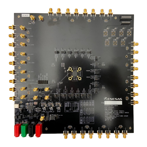
1. Configure the lab power supply to 3.3V with a 700mA limit. Turn off the output.
2. Set POWER_SEL (JP21) to select VCC_INPUT.
3. Remove all output terminations.
4. Set Dip Switch selectors to the positions shows in Figure 3.
5. Connect VEE to the GND jack (J22).
6. Connect the 3.3V source to POWER (J90).
7. Turn on the power supply. The current should measure ~503mA.
Optional (for I2C programming through Timing Commander).
8. Connect a cable from a PC to the USB port.
When correct operation is verified, set the power supply limit for the number of outputs to be active.
The board ships with a 50MHz crystal and with the DIP Switch settings from Figure 3 it will be configured as
follows:
▪ QA1 = QA2 = 156.25MHz, LVDS levels
▪ QB1 = QB2 = 156.25MHz, LVPECL levels
▪ QC0 = QC1 = 125MHz, LVDS levels
▪ QD0 = 125MHz, LVDS levels
▪ QD1 = High Impedance
When evaluating performance with the default hardware configuration, it is recommended that all active outputs
be terminated 50Ω to GND by either terminator plugs or an instrument.
Bank A: This device supports four outputs for bank A, but only QA1 and QA2 have been routed. This bank's
termination is configured for LVDS operation and will not switch if set to LVPECL levels unless the terminations
are modified. For LVPECL operation, consult Output Configuration.
Bank B: This device supports four outputs for bank A, but only QB1 and QB2 have been routed. This bank's
termination is configured for LVPECL operation. For LVDS operation, consult Output Configuration.
Bank C: This bank's termination is configured for LVDS operation and will not switch if set to LVPECL levels
unless the terminations are modified. For LVPECL operation, consult Output Configuration.
Bank D: QD0 is terminated for LVDS operation and will not switch if set to LVPECL levels unless the terminations
are modified. For LVPECL operation, consult Output Configuration.
1.2 Board Power Supply
This board offers the option to power the device from either a supply set to 5V and an LDO (U9), or the supply set
to 3.3V and bypassing the LDO.
1.2.1 Bypass External LDO (Default Configuration)
Set JP21 jumper to VCC_INPUT. Provide 3.3V to the POWER jack (J90).
1.2.2 External LDO Configuration
Set JP21 jumper to VCC_LDO. Provide 5V to the POWER jack (J90).
