AN1038 Rev 0.00 Page 10 of 14
Sep 2002
Back to Back Configuration
Description
The back to back configuration connects two evaluation boards
together at the PCM interface. The PCM output data from one
board is the PCM input data to the other board. One board is
configured as a master for clock generation and the other is
configured as a slave. A secondary power cable provides daisy
chain power to the second evaluation board.
Power Supply Connections
Power should be applied to the evaluation board using the
primary power cable. Either J5 or J6 may be used. Prior to
applying power, the voltage setting of each supply should be
verified. The power supplies should be turned off while mating
the power cables to the evaluation boards.
Jumper Settings
All jumper settings are described below.
In this configuration the master board provides the clock and
frame sync to the slave board. The selection of the clock rate is
arbitrary and may be any of the available frequencies.
The ribbon cable used to connect the two boards at J14 also
connects the ground planes of the two evaluation boards.
Having returns adjacent to the high speed clock edges is
critical to reducing board level noise.
If transmission quality is poor verify both master and slave
boards are set up for same coding scheme, JP8. In addition,
verify the transhybrid jumper, JP7, is inserted in both boards. If
signal quality still does not improve, verify JP12 of the slave
board is not populated.
Analog to Analog Verification
The back to back configuration verifies the complete signal
path of two evaluation boards. Full duplex transmission is
provided from one Tip and Ring interface to the other. Both
ISL5585 devices do not have to be in the same transmission
mode (forward, reverse or teletax) for proper back to back
operation.
SECONDARY POWER CABLE
MASTER
SLAVE
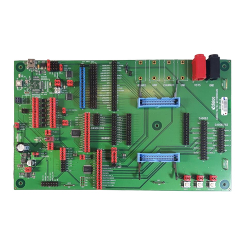
FIGURE 15. BACK TO BACK CONNECTORS AND JUMPERS
010x11
01x1 00
0
TABLE 5. MASTER BOARD JUMPER POSITIONS
JUMPER DESCRIPTION
JP4 Connects the receive output of the CODEC (U6) to
the device receive input -IN through RIN.
JP6 Connects the device transmit output VTX to the
CODEC amplifier for transhybrid balance.
JP7 Connects the receive output of CODEC to
transhybrid amplifier, AC coupled by C1.
JP10, POSN 2 Sets the CODEC master clock to 512kHz.
JP11 Enables the on board logic multiplexer.
JP12 Configures board as master.
TABLE 6. SLAVE BOARD JUMPER POSITIONS
JUMPER DESCRIPTION
JP4 Connects the receive output of the CODEC (U6) to
the device receive input -IN through RIN.
JP6 Connects the device transmit output VTX to the
CODEC amplifier for transhybrid balance.
JP7 Connects the receive output of CODEC to
transhybrid amplifier, AC coupled by C1.
JP11 Enables the on board logic multiplexer.
