AN1957 Rev 0.00 Page 2 of 6
September 5, 2014
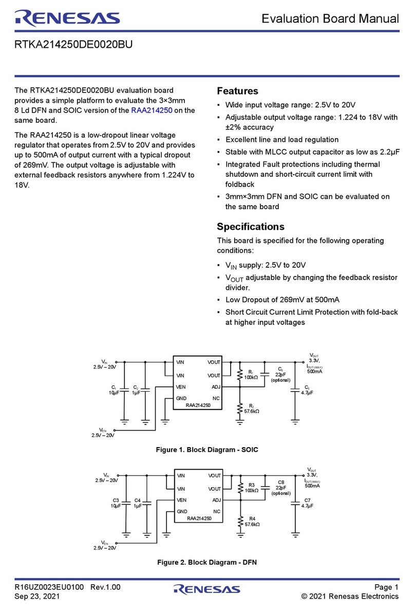
ISL91134IIQ-EVZ
Functional Description
The ISL91134 implements a complete boost switching regulator,
with PWM controller, internal switches, references, protection
circuitry and bypass control. The ISL91134 is designed to support
5V output voltage. A voltage select pin (VSET) is available to scale
up the output voltage by a small offset to compensate the load
transient droop. The evaluation boards have been functionally
optimized for best performance of the ISL91134. This part
requires only an inductor and a few external components to
operate. The 2.5MHz switching frequency further reduces the
size of external components. The input power and load
connections are provided through multi pin connectors for high
current operations.
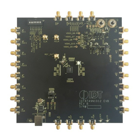
The ISL91134 evaluation board is shown in Figures 3 and 4. The
board’s enable function is controlled by the on-board jumper header
J3. Similarly, the VSET function is controlled by the on-board jumper
header J4 and the BYPASS function can be set to Forced or Auto
mode by controlling the on-board jumper header J5.
The schematic of the ISL91134-EVZ evaluation board is shown
on page 4.The PCB layout images for all layers are shown in
Figures 5 and 6. The bill of materials of the ISL91134-EVZ is
shown in Table 1.
Operating Range
The VIN range of the boards is 2.35V to 5.4V. The VOUT for the
ISL91134 is 5V. The IOUT range of the boards is 0 to 2A. The
operating ambient temperature range is -40°C to +85°C.
Quick Start Guide
For the ISL91134 board, the voltage can be set to 5V with
VSET = 0 and 5.2V with VSET = 1.
Refer to the following Quick Setup Guide to configure and
power-up the board for proper operation. During the power-on
process, the expected waveforms are shown in Figure 2.
Quick Setup Guide
1. Install jumpers on J3 shorting EN to VIN.
2. Install jumper on J5 shorting BYPS to VIN, auto bypass mode.
3. Install jumper on J4 shorting VSET to GND or leave it as NC.
4. Connect power supply to J1, with voltage setting between
2.35V and 5.4V.
5. Connect electronic load to J2.
6. Place scope probes on VOUT test point, and other test points
of interest.
7. Turn on the power supply.
8. Monitor the output voltage VOUT = 5.05V when VIN < 5V (Boost
mode), VIN = VOUT when VIN > 5.15 (bypass mode), the supply
current should be ~110µA (boost mode) and ~95µA in (auto
bypass mode). In forced bypass (BYPS pin = GND), supply
current should be ~45µA.
9. Turn on the electronic load.
10. Measure the output voltage with the voltmeter. The voltage
should regulate within data sheet spec limits.
11. To determine efficiency, measure input and output voltages
at the test points J1 and TP3. The bench power supply can be
connected to the PVIN and GND headers on J1. The electronic
load can be connected to the VOUT and GND headers on J2
measure the input and output currents. Calculate efficiency
based on these measurements.
Layout Considerations
1. C1is used to compensate for line drops on cables from power
supply to the IC, this will not be required for the actual board
design.
2. The Input capacitor (C2) should be placed close to the IC to
reduce VIN spikes/noise.
3. Output capacitors (C3, C4) should be placed as close as
possible to the IC to minimize VOUT spikes.
4. Boost Inductor (L1) between VIN and LX should be connected
using short and wide traces. It is recommended to use
multiple vias between the LX pin and the inductor. Three vias
of 7mils width were used on the evaluation board.
5. Recommend maximizing copper pour area for VIN, VOUT and
GND for better thermal performance.
6. AGND and PGND of the IC should be connected to each other.
It is crucial to connect these two grounds at a location very
close to the IC.
FIGURE 2. START-UP WAVEFORM 50ΩLOAD

