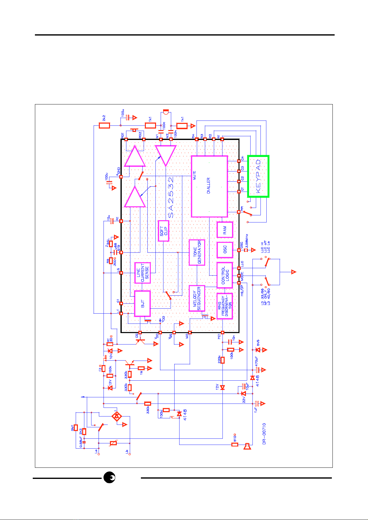
Sames SA2532 User manual

sames
SA2532
1/22
sames
VERSATILE SINGLE CHIP TELEPHONE
4153
SA2532 A/C/U
PDS039-SA2532-001 Rev. C 23-10-1995
FEATURES
nSpeech circuit, LD/MF Dialler and Tone
Ringer on one 28 pin CMOS chip
nSoft clip to avoid harsh distortion
nLine Loss Compensation selectable by
pin option
nPower down mode
nVersatile applications for different PTT
demands
n31 digit last number redial
nSliding Cursor protocol with comparison
n2 Flash keys, 100 ms and 280 ms (option
600 ms)
nPause key for 3 sec Auto Pause or Wait
Function
nRing frequency discrimination
nOperating range from 13 to 100 mA
(down to 5 mA with reduced perform-
ance)
nLow noise (max. -72dBmp)
nReal or Complex impedance on chip pro-
grammable
nLD/MF switchable dialling
nOn chip MF filter (CEPT CS 203 compat-
ible)
n3-tone melody generator with selectable
repetition rates
1/22
GENERAL DESCRIPTION
TheSA2532isaCMOSintegratedcircuitthat
contains all the functions needed to form a
high performance electronic telephone.
The device incorporates LD/MF dialling,
melody generation, ring frequency discrimi-
nation and a high quality speech circuit.
A RAM is on chip for a 31 digit last number
redial. The sliding cursor procedure makes
Last Number Redial easy behind a PABX.
The versatility of the circuit is provided by on
chipprogrammabilityandafewexternalcom-
ponents. This allows easy adaption to differ-
ent PTT requirements without changing the
PCB of the telephone.
PACKAGE
Available in 28 pin DIP and SOIC
SA2532
HS DP
DR-00975
OSC
C3
C4
RR
14
AGND
STB
LLC
CI
MO
DD
RO2
RO1
LS
V
1
R2
15
R4
R3
C1
C2
M2
MODE
M1
FCI
R1
28
SS
V
CS
RI
LI

2/22
SA2532
sames
PIN DESCRIPTION
Pin# Symbol Function
23 M1 Microphone Inputs
24 M2 Differential inputs for the microphone (electret).
3 RO1 Receiver Outputs
2 RO2 These are the outputs for driving a dynamic earpiece with an impedance
of 100 to 300Ω
5A
GND Analog Ground
This is the analog ground for the amplifiers.
28 RI Receive Input
This is the input for the receive signal.
6STBSide Tone Balance Input
This is the input for side tone cancellation.
1LS Line Current Sense Input
This is the input for sensing the line current.
27 LI Line Input
This input is used for power extraction and line current sensing.
25 CS Current Shunt Control Output
This N-channel open drain output controls the external high power shunt
transistor for the modulation of the line voltage and for shorting the line
during make period of pulse dialling.
4V
DD Positive Voltage Supply
This is the supply pin for the circuit.
26 VSS Negative Power Supply
8MO Melody Output
Pulse Density Modulated output of the melody generator for tone ringer. At
high impedance when not active.
21 FCI Frequency Comparator Input
This is a Schmitt trigger input for ring frequency discrimination. Disabled
during off-hook.
10 HS/DP Hook Switch Input and Dial Pulse Output
This is an I/O that is pulled high by the hook switch when off- hook. An open
drain pulls it low during break periods of pulse dialling and flash.
11 OSC Oscillator Input
Oscillator pin for Xtal or ceramic resonator (3.58 MHz).
9 LLC Line Loss Compensation
Select pin for line loss compensation.
12 RR Repetition Rate
Select pin for repetition rate of melody.
22 MODE Signalling Mode Select Input
Mode pin Function
High LD default mode, make/break = 33/66 ms
Open MF only
Low LD default mode, make/break = 40/60 ms
20 R1 Keyboard Rows
19 R2
18 R3
17 R4
16 C1 Keyboard Columns
15 C2
14 C3
13 C4
7CI Complex Impedance Input
Input pin for the capacitor in the complex impedance

sames
SA2532
3/22
FUNCTIONAL DESCRIPTION
Power On Reset
The on chip power on reset circuit monitors the supply voltage (VDD). When VDD rises above
approx. 1.2V, a power on reset occurs to assure correct start-up and the RAM is cleared.
DC Conditions
The normal operating range is from 13mA to 100 mA. Operating range with reduced
performance is from 5mA to 13mA. In the operating range all functions are operational.
In the line hold range from 0 to 5 mA the device is in a power down mode and the voltage at
LI is reduced to maximum 3.5V.
The dc characteristic (excluding diode bridge and Pulsing transistors) is determined by the
voltage at LI and the resistor R1 as follows:
VLS = VLI + I
Line
.R1
The voltage at LI is 4.5V.
During pulse dialling the speech circuit and other parts of the device not required are in a
power down mode to save current. The CS pin is pulled to VSS in order to turn the external
shunt transistor on to keep a low voltage drop at the LS pin during make periods.
AC Impedance
The Characteristic or Output impedance of the SA2532 is set within the IC and adjusted by
MaskOptions. Availableoptionsarefor600Ωand1000Ω. Whenthe1000Ωoptionisselected
then a capacitor may be added to the circuit at pin CI to add a reactive element and make the
output impedance complex.
Oscillator
AlltheTimingFunctionsoftheSA2532arebasedonaClockFrequencyof3.58MHz. Acrystal
orceramic resonatorof thisfrequency shouldbe connectedto theOSC pin. Inpractise minor
deviations from the nominal frequency may occur due to the characteristics of the frequency
reference device used and so it is recommended that care is taken in the selection of
components.
In some cases a small value capacitor (≤47pF) mayhavetobe connected inparallelwith the
Frequency Reference to ensure start-up and/or operation at the nominal frequency.
Speech Circuit
The speech circuit consists of a transmit and a receive path with soft clip, mute, line loss
compensation and side tone cancellation.
Transmit
The gain of the transmit path is 35 dB for M1/M2 to LS (see test circuit figure 5). The
microphone input is differential with an input impedance of 25 kΩ.
Thesoftclipcircuitlimits theoutput voltageatLIto2.0VPEAK. Theattacktimeis30µs/6dB
and the decay time is 20 ms/6 dB. When mute is active, during dialling or after pressing
the MUTE key, the gain is reduced by > 60 dB.

4/22
SA2532
sames
Receive
The receive input is the differential signal of RI and STB. The gain of the receive path is
2dB(testcircuitfigure5)withdifferentialoutputs,RO1/RO2(0dBonSA2532C/U). When
mute is active during dialling the gain is reduced by > 60dB. During DTMF dialling a MF
comfort tone is applied to the receiver. The comfort tone is the DTMF signal with a level
that is -30dB relative to the line signal.
Side Tone
Side Tone is controlled along with Return Loss by a Double Balance Bridge as shown in
Fig. 1. Figure 1
Double balance bridge (return loss and side tone) with one common ground
A good side tone cancellation is achieved by using the following equation:
ZBAL = R5
ZLINE R1
The side tone cancellation signal is applied to the STB input.
Line Loss Compensation
When Line Loss Compensation is active the gain of the Transmit and Receive amplifiers
are changed by 6dB in accord with the DC conditions as measured at Pins LI and LS.
WhentheLLCPinisLowthisadjustmentingainoccursovertherangeILINE =20to50mA.
When LLC is High the range is 45 to 75mA. Note that these figures apply for R1 = R30Ω.
WhentheLLCPinis opentheamplifiergainsremain fixedregardlessoftheLine Current.
ONE COMMON GROUND
Z
BAL
DR-00708
RETURN LOSS
LINE
V
Z
REF
SS
R2
R1
RI
SIDE TONE
R5
STB
SYN
LI

sames
SA2532
5/22
Dialling Functions
Valid Keys
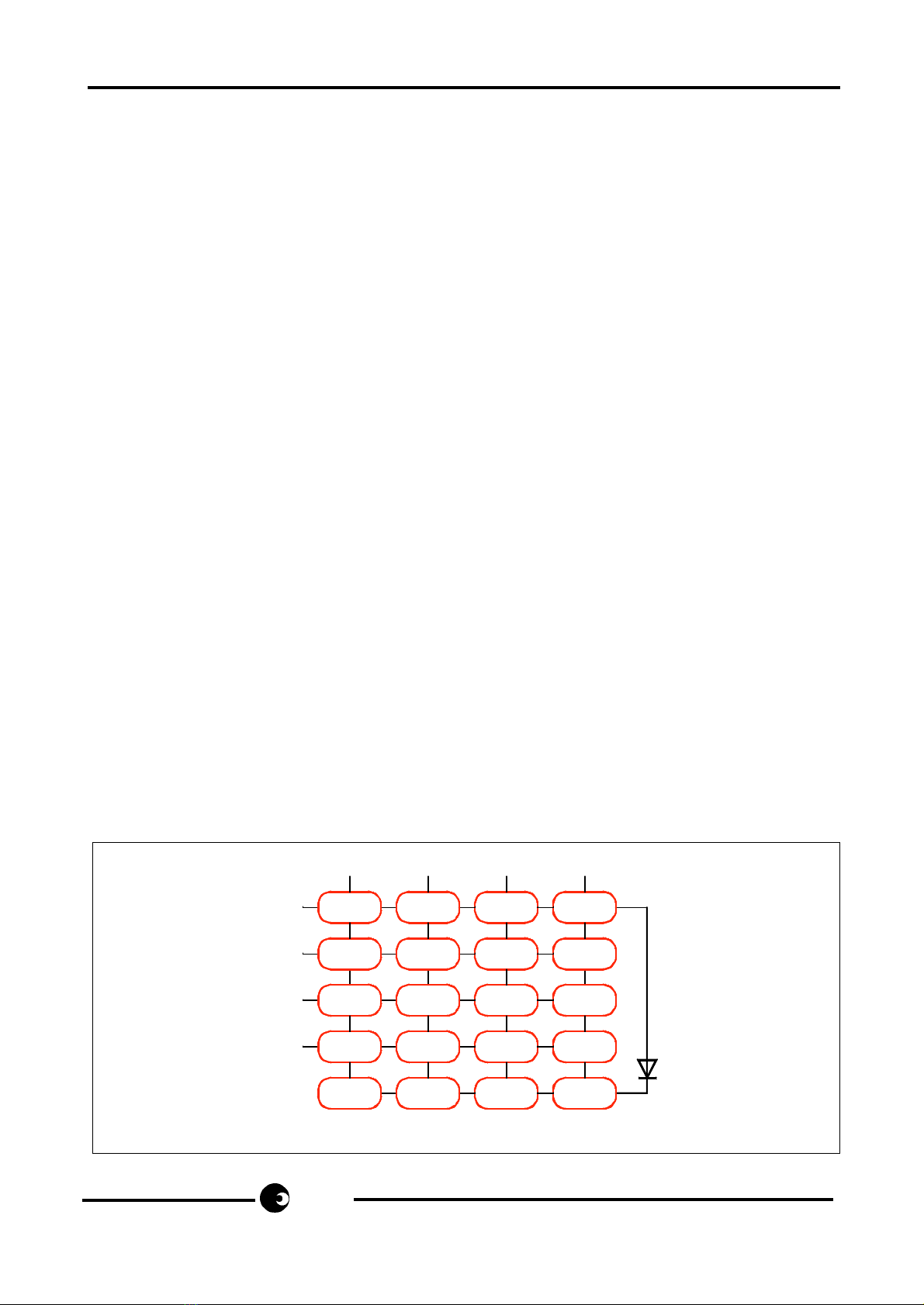
ThekeypadoftheSA2532comprisesamaximumof20keys(ofwhich3havenofunction).
A Bi-polar scan technique is used so that the 20 keys are scanned in a 4 x 5 matrix using
only 8 pins.
AvalidkeyisdetectedwhenoneandonlyonecontactclosureisdetectedbetweenaRow
and Column Pin. Key contacts are debounced to avoid incorrect detection.
Dial Mode Selection
The default mode (LD or MF) can be selected by the Mode pin. When default LD mode
is selected, a temporary change to MF can be invoked by pressing the * key. The circuit
will revert to LD by pressing the R (or R2) key or by next on-hook.
When MF mode is selected by the mode pin, the circuit can not be changed temporarily
to LD but will remain in MF.
Last Number Redial
LNRisafacilitythatallowsresignallingofthelastmanuallydiallednumberwithoutkeying
in all the digits again. The LNR is repeatable.
The current contents of the RAM are overwritten by new entries.
A manually entered number is automatically stored in the LNR RAM. The capacity of the
RAM is 31 digits. If a number greater than 31 digits is entered, the LNR facility will be
inhibited(Untilnewentries<32digits)andfurtherentrieswillbebufferedin aFirstInFirst
Out Memory (FIFO).
Postdialleddigits,i.e.digitsmanuallyenteredafterLNRhasbeeninvoked,arenotstored
in RAM but buffered in FIFO.
During dialling, one or more pauses can be inserted by pressing the PAUSE KEY. Each
pauseis3secs(optionally6secs)wheninsertedwithinthefirst5digits. OtherwiseaWait
Function will halt dialling until the LNR Key is pressed.
Recall Function
A Recall (R key or R2 key) activation will invoke a Flash (Timed Loop Break).
If Recall is the first entry in a digit string, it will be stored in LNR RAM when digit(s) are
entered after the Recall.
If the recall key is depressed after a digit string has been entered or dialled out, the recall
will not be stored but buffered in the FIFO together with subsequently entered digits.
If pressing the recall key is not followed by digit entries, the LNR RAM remains intact.
After a recall, a 3 second pause will automatically be executed.
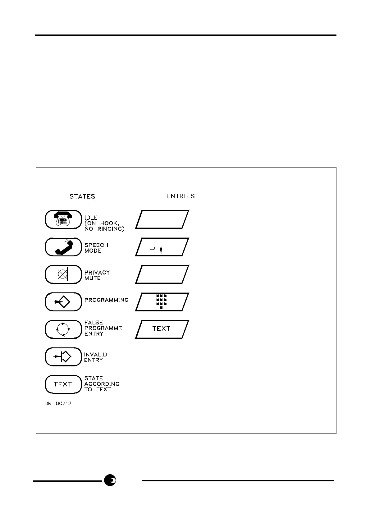
Mute Function
The MUTE key is enabled in speech mode only. Depressing the MUTE key mutes the
microphone amplifier. Repressing the MUTE key deactivates the mute (toggle function).
AnykeyentryoverwritesamuteactivatedbytheMUTEkeyandmutewillbedeactivated.
When privacy mute is activated a reminder tone is applied to the earpiece every 3
seconds.

6/22
SA2532
sames
Sliding Cursor Procedure
To accommodate easy and uncomplicated redialling (LNR) behind a PABX, a sliding
cursor protocol is implemented. If new entries match the previous RAM contents,
pressing the LNR key will dial out the remaining digits.
If there is an error in matching, the LNR will be inhibited until next on-hook, and the RAM
will contain the new number.
Tone Generator
The tone generator incorporates the DTMF tones and 3 basic frequencies for the tone
ringer.
DTMF Tones
The DTMF Tone Generator creates 12 Tones in compliance with CCITT Recommenda-
tion Q23. Signal levels are altered by Mask Option. High group frequencies have a level
2.6dB higher than those of the Low Group.
Details of the DTMF Tones are:
Low group Digit 1-2-3 697Hz (Error = -.074%)
Digit 4-5-6 770Hz (Error = -.679%
Digit 7-8-9 852Hz (Error = -.621%)
Digit *-0-# 941Hz (Error = +.139%)
High group Digit 1-4-7-* 1209Hz (Error = +.533%)
Digit 2-5-8-0 1336 Hz (Error = +.176%)
Digit 3-6-9-# 1477Hz (Error = -.141%)
Errors are calculated with reference to a base clock of 3.58MHz and at ambient
temperature of 24°C. They exclude tolerance errors in the base frequency.
KEYBOARD ARRANGEMENT
Figure 2
DR-00709
R3
R4
LNR/CONT.
#
8 9
PAUSE
R2
R1
C1
4
MUTE
C2
5
1
R
0
R2
*
C3
6
2
C4
7
3

sames
SA2532
7/22
Microcontroller Interface
ThekeypadRowandColumnPinscanreadilybedrivenby aMicrocontrollerInterface. When
configured in this way the SA2532 inputs and dials the corresponding digits in either LD or
DTMF. The LNR store can be used to buffer digits to allow high speed data entry. See
Application Note AN3002A for details.
Tone Ringer
The Tone Ringer of the SA2532 incorporates a Discriminator Circuit and adjustable Melody
Generator
Ring Frequency Discrimination
The Ring Frequency Discriminator assures that only signals with a frequency between
20Hz and 60Hz (option 13 Hz to 60 Hz) are regarded as valid ring signals.
When a valid ring signal is present for 73ms continuously, the melody generator is
activated and remains active as long as the ring signal is present.
Once the melody generator has been started, the ring signal is continuously monitored
and the melody generator is instantly turned on or off according to the momentary
presence of a valid or unvalid ring signal respectively (until next POR or off-hook).
Melody Generator
When a Valid Ring Signal is detected the Melody generator is activated and creates a
ringing Signal comprising 3 frequencies F1 (1065Hz), F2 (1420Hz) and F3 (1734Hz).
These frequencies are repeated in a sequence of 6 time slots constructed by the
frequencies
F1 F2 F3 F1 F2 F3
This sequence is repeated 1, 4, 7 or 10 times per second as indicated by the connection
of the RR Pin to one of the four rows of the keyboard.

8/22
SA2532
sames
TYPICAL APPLICATION
Only the components necessary for presenting the complete functions of the SA2532 are
included. FIGURE 3

sames
SA2532
9/22
FEATURE PHONE APPLICATION
Only the components necessary for presenting the complete functions of the SA2532 are
included. FIGURE 4

10/22
SA2532
sames
OPERATING PROCEDURES
Procedure Principles
The procedures for utilizing the features of the SA2532 are optimized out of consideration for
the human factor in order to:
- meet the user’s expectations
- be easy to learn and relearn
- not invoke any automatic functions which the user doesn’t expect
- protecttheuserfromcommittingcriticalerrors,e.g.diallingwrongnumbers,deletingstored
numbers, etc.
- be consistent, simple and usable
SYMBOLS

sames
SA2532
11/22
Privacy Mute

12/22
SA2532
sames
Temporary MF
FIFO
Pressing any other
key does not
change the state.
EXIT FIFO

sames
SA2532
13/22
TIMING DIAGRAMS
MF Dialling
LD Dialling
LD Dialling with Access Pause

14/22
SA2532
sames
ELECTRICAL CHARACTERISTICS
Absolute Maximum Ratings
PositiveSupplyVoltage.......................................................................................-0.3V≤VDD≤7V
Inputcurrent..................................................................................................................±25mA
InputVoltage(LS)..............................................................................................-0.3V≤VIN≤10V
InputVoltage(LI,CS)...........................................................................................-0.3V≤VIN≤8V
InputVoltage(STB,RI)..............................................................................-2V≤VVIN≤VDD+0.3V
InputVoltage(MO).............................................................................................-0.3V≤VIN≤35V
DigitalInputVoltage...................................................................................-0.3V≤VIN≤VDD+0.3V
ElectrostaticDischarge...................................................................................................±800V
StorageTemperature......................................................................................-65°Cto+125°C
Recommended Operating Conditions
SupplyVoltage*(SpeechMode)..........................................................................4V≤≤
≤≤
≤VDD≤5V
OscillatorFrequency(Resonator: MurataCSA3.58MG312AM)..........................3.58MHz
OperatingTemperature...................................................................................-25°Cto+70°C
* This voltage is generated internally
DC Characteristics (ILINE = 15 mA unless otherwise specified)
Symbol Parameter Conditions Min Typ Max Units
IDD Operating Current Speech mode 3 5 mA
MF dialling 4 mA
LD dialling VDD = 2.5V 200 µA
Ring mode VDD = 2.5V 300 µA
IDDO Retention Current Idle mode VDD = 2V, 0.05 µA
TAMB = 25°C
VLI Line Voltage (default) 13mA≤ILINE ≤100mA 4.5 V
IOL Output Current, Sink VOL = 0.4V 1.5 mA
CS,HS/DP,MO
Flash

sames
SA2532
15/22
AC Characteristics (ILINE=15mA;f=800Hz unless otherwise specified)
Symbol Parameter Conditions Min Typ Max Units
TX Transmit Test Circuit Fig.5
ATX Gain (M1/M2) ZRL=600Ω34 35 36 dB
ZRL = 1000Ω36.5
ATX/F Variation with Frequency f=500Hz to 3.4kHz ±0.8 dB
THD Distortion VLI≤0.5VRMS 2%
V
AGC Soft Clip Level VLI=2V
PEAK
ASCO Soft Clip Overdrive 20 dB
tATTACK Attack Time 30 µs/6dB
tDECAY Decay Time 20 ms/6dB
ZIN Input Impedance (M1/M2) 20 kΩ
AMUTE Mute Attenuation Mute activated 60 dB
VNO Noise Output Voltage -72 dBmp
VFC Unwanted Frequency 50...300 Hz -43 dBm
Components 4.3...28 kHz note 1
above 28 kHZ -70 dBm
VINMAX Input Voltage Range Differential ±1 VPEAK
(M1/M2) Single Ended ±0.5 VPEAK
BJT Output Driver
VINMAX Input Voltage Range (LI) ±2 VPEAK
VTX Dynamic Range ±2 VPEAK
RL Return Loss ZRL = 600ΩSA2532A 18 dB
ZRL = 1000ΩSA2532C/U
Note 1: -37 dBm at 4.3 kHz and decreasing 12 dB/octave till 28 kHz.

16/22
SA2532
sames
AC Characteristics (cont’d) (ILINE = 15 mA;f=800Hz unless otherwise specified)
Symbol Parameter Conditions Min Typ Max Units
RX Receive Test Circuit Fig.5
ARX Receive Gain (RO1/RO2) ZRL=600Ω12 3dB
Z
RL=1000Ω-0.2
∆ARX/F Variation with Frequency f=500 Hz to 3.4 kHz ±0.8 dB
THD Distortion VRI≤0.5VRMS 2%
V
AGC Soft Clip Level VRI=1V
PEAK
ASCO Soft Clip Overdrive 10 dB
tATTACT Attact Time VRI>0.8V 30
µs/6dB
tDECAY Decay Time 20
ms/6dB
VNO Noise Output Voltage -72 dBmp
VFC Unwanted Frequency 50 Hz...20 kHz -60 dBm
Components
ZIN Input Impedance (RI) 8 kΩ
VIN RI Input Voltage Range(RI) ±2 VPEAK
ST Sidetone Test Circuit Fig.5
AST Sidetone Cancellation VRI≤0.5VRMS 26 dB
VIN ST
Input Voltage Range (STB)
±2 VPEAK
ZIN Input Impedance (STB) 80 kΩ
Keyboard
tDKey Debounce Time 15 ms
HS Input
tHS-L Low to High Debounce Going off-hook 15 ms
tHS-H High to Low Debounce Line breaks/on-hook 240 ms
DTMF
∆ F Frequency deviation Note 5 -.679 +.533 %
VMF
MF Tone Level(Low group)
Optionally -12.5 -11 -9.5 dB
-9.5 -8 -6.5 dB
VL-H Preemphasis Low to High 2.0 2.6 3.0 dB
THD Distortion Note 3 -30 dBr
tTD Tone Duration Note 1 80 82.3 85 ms
tITP Inter Tone Pause 80 82.3 85 ms

sames
SA2532
17/22
AC Characteristics Cont'd
Symbol Parameter Conditions Min Typ Max Units
tTR Tone Rise Time Note 2 5 ms
tTF Tone Fall Time Note 2 5 ms
LD
tDR Dial Rate ±5% 10 pps
tM/B Make/Break Period ±5%, MODE=low 40.8/61.2 ms
±5%, MODE=high 33/66 ms
tPDP Pre-Digit Pause 35 ms
tIDP Inter Digit Pause 800 840 880 ms
tMO Mute Overhang tM
tFD Flash Duration 1 100 102 ms
Flash Duration 2 SA2532A/C 270 300 ms
Flash Duration 2 SA2532U 600 650 ms
tPFP Post Flash Pause 2.9 3.0 3.1 sec.
tAP Access Pause Period SA2532A/U 2.9 3.0 3.1 sec
SA2532C 5.8 6.0 6.2 sec
Tone Ringer
VMO Melody Output Level PDM
tMD Melody Delay 10 ms
F1 Frequency 1 1020 1064 1107 Hz
F2 Frequency 2 1363 1420 1477 Hz
F3 Frequency 3 1665 1734 1803 Hz
tDT Detection Time Initial 70 80 ms
tTO Detection Time-out note 4 ms
fMIN Min. Detection Frequency 19 20 21 Hz
fMIN Min. Detection Frequency Optionally 12 13 14 Hz
fMAX Max. Detection Frequency 58 59 60 Hz
Reminder Tone
VRT Level (RO1/RO2) Relative to LS -30 dBr
tRTD Duration 82.3 ms
tRTI Interval 3 sec
Comfort Tone (DTMF)
VCT Level (RO1/RO2) Relative to LS -30 dBr

18/22
SA2532
sames
Note 1: The values are valid during automatic dialling and are minimum values during
manual dialling, i.e. the tones will continue as long as the key is depressed.
Note 2: Therisetimeisthetimefrom10%offinal valueuntilthetoneamplitudehasreached
90% of its final value.
Note 3: Relative to high group.
Note 4: TheFCIcircuit isresetby PORandHS/DP pulledhigh(off-hook). Afterareset the
FCI circuit is in a standby state. A positive edge on FCI will start a 73ms timer and
the frequency discrimination is initiated. Whenever a period of the ring signal is
missing, the timer is reset. When a valid ring signal is present for ≥ 73ms, the
melody generator is started and is directly controlled by the ring signal. This
condition will remain until a new reset.
Note 5: This does not include the frequency deviation of the ceramic resonator.

sames
SA2532
19/22
Test Circuit
Figure5

20/22
SA2532
sames
Ordering Information:
Versions ZRL DTMF R2 Access Package
(ohm) Level Period Pause
SA2532A P 600 -6/-8dBm 280ms 3s 28 pin DIP
SA2532A S 600 -6/-8dBm 280ms 3s 28 pin SOIC
SA2532C P 1000 -6/-8dBm 280ms 6s 28 pin DIP
SA2532C S 1000 -6/-8dBm 280ms 6s 28 pin SOIC
SA2532U P 1000 -9/-11dBm 600ms 3s 28 pin DIP
SA2532U S 1000 -9/-11dBm 600ms 3s 28 pin SOIC
This manual suits for next models
6
Table of contents