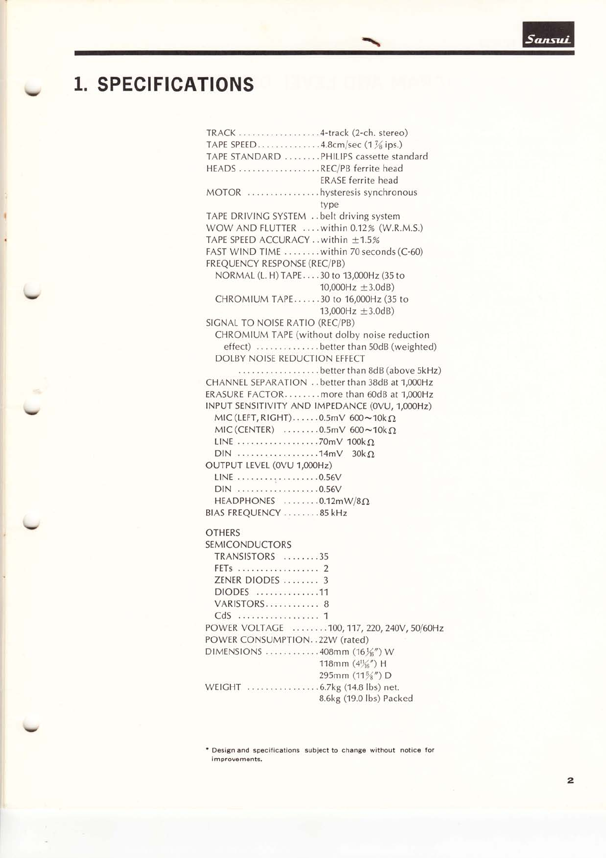
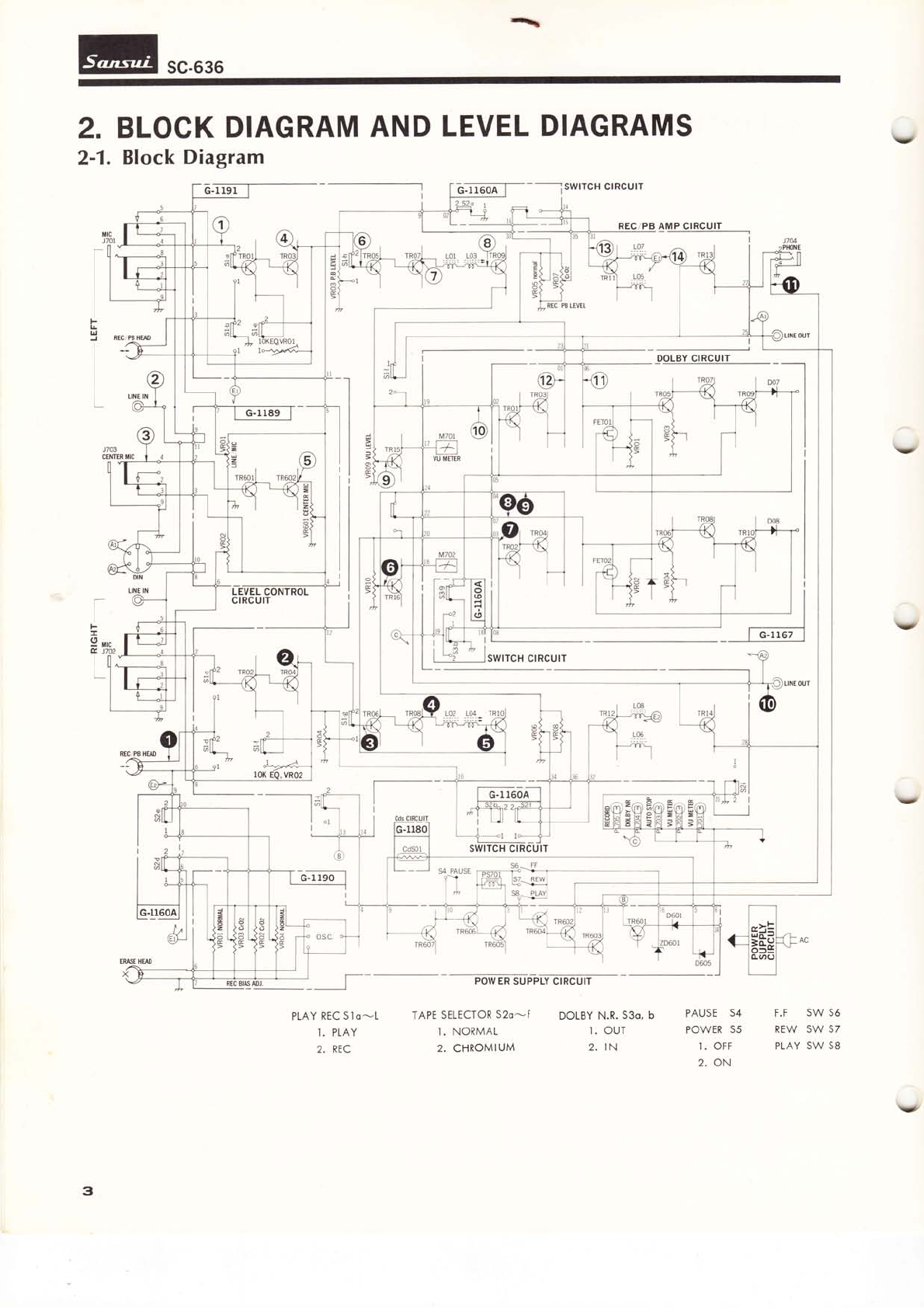
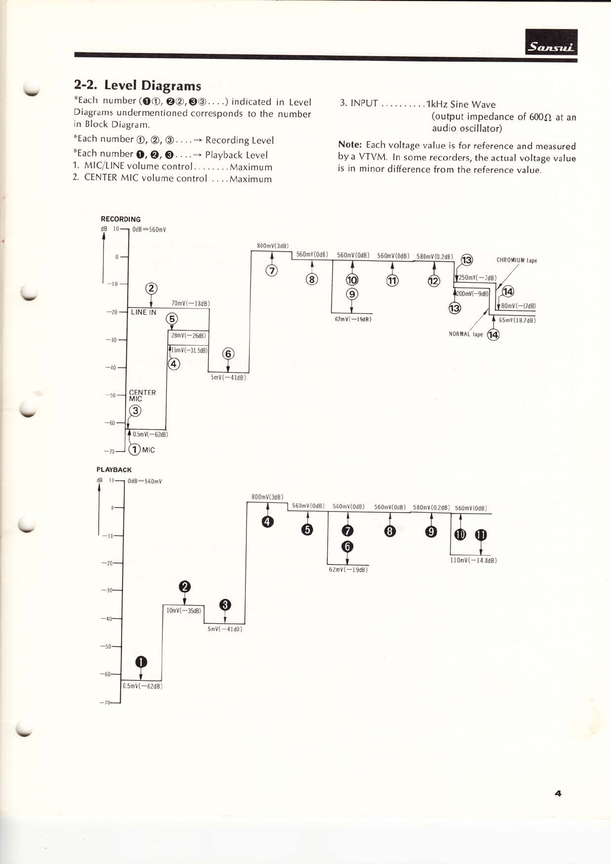
sG-636
3-6-2. Setting TAPE SELECTOR switch to
CHROMIUM
1) Perform steps 1) throrgh 3) of 3-6-1.
2) Push on the PAUSE button and set the unit in the
record mode using the Chrom iu m test tape (SCT-
FCR).
3) Perform steps 5), 6) and 7) of 3-6-1.
4) lf the indication of output level on each channel is
under 56mV, turn VR07 for L-ch and VROB for R-ch
on C-1191 counterclockwise or if it is over 56mV,
turn them clockwise from conductor side so that the
output level 56mV may be exactly obtained.
Repeat the above step 3) a few times until the
indication on VTVM will be exactly 56mV.
3-7. Dolby Circuit Adiustment
(See FiS. 3-4)
1) Set the MICiLINE LEVEL volume to maximum and
DOLBY switch to OUT.
2) Turn VR01 clockwise (viewed from the bottom side)
and VR02 counterclockwise (viewed from the bottom
side.)
3) Connect a VTVM respectirely between the terminal
01 and ground for L-ch, and terminal 04 and ground
for R-ch on F-1 167.
4) Supply the 5kHz signal from an audio signal genera-
tor to the LINE INPUT terminals (1, R-ch).
5) Push on the PAUSE button and set the unit in the
record mode after setting a Normal test tape (SCT-
FC86)
6) Adjust the output level volume of the audio signal
generator for obtaining 17.SmV on the VTVM.
7) Cround TP01 and TP02 and set the DOLBY switch to
tN.
B) Adjust VR03 for L-ch, and VR04 for R-ch on F-1167
until the VTVM reads 55.3mV (+10d8) higher posi-
tion from 17.smV.
9) Disconnect TP01 and TP02 from ground.
10) Adjust VR01 for L-ch, and VR02 for R-ch on F-1167
until the VTVM reads 4O.9mV (-2dB) lower posi-
tion from 55.3mV.
11) Cround TP01 and TP02 again.
Make sure that the VTVM connected between the
terminal 01 and ground for L-ch, and the 04 and
ground for R-ch reads 55.3mV (+ 2dB) higher posi-
tio n.
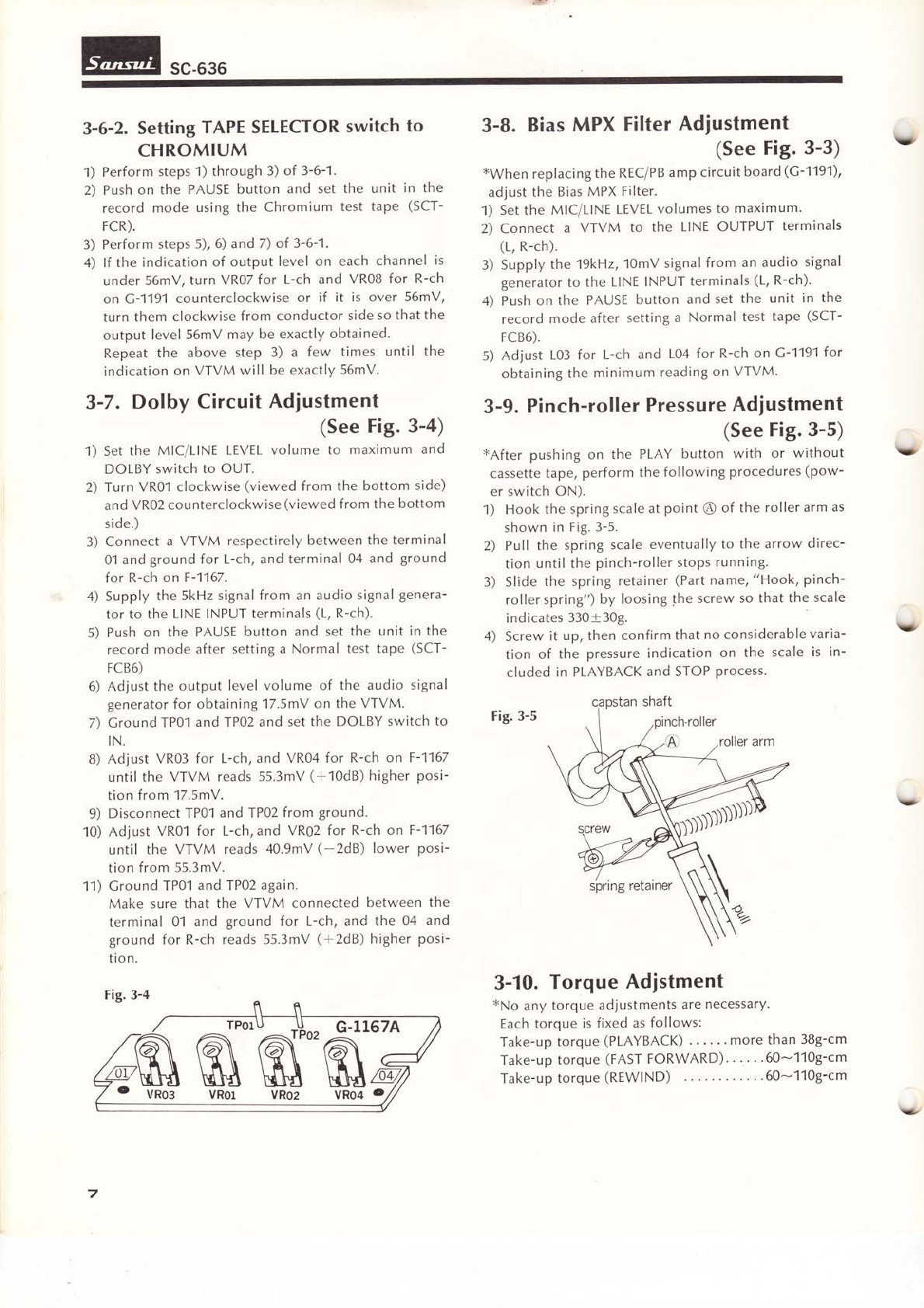
tig. 3-4
3-8. Bias MPX Filter Adiustment
(See tig. 3-3)
*When replacing the RE CIPB amp circuit board (C -1191),
adjust the Bias MPX Filter.
1) Set the Mlc/LINE LEVEL volumes to maximum.
2) Connect a VTVM to the LINE OUTPUT terminals
(1, R-ch).
3) Srpply the 19kHz,10mV signal from an audio signal
generator to the LINE INPUT terminals (1, R-ch).
4) Push on the PAUSE button and set the unit in the
record mode after setting a Normal test tape (SCT-
FC86).
5) Adjust 103 for L-ch and 104 for R-ch on C-1191 Íor
obtaining the minimum reading on VTVM.
3-9. Pinch-roller Pressure Adiustment
(See Fig. 3-5)
*After pushing on the PLAY button with or without
cassette tape, perform the following procedures (pow-
er switch ON).
1) Hook the spring scale at point @ of the roller arm as
shown in Fig. 3-5.
2) Pull the spring scale eventually to the arrow direc-
tion until the pinch-roller stops running.
3) SIide the spring retainer (Part name, "Hook, Pinch-
roller sprin g") bY loosing the screw so that the scale
indicates 330+308.
4) Screw it up, then confirm that no considerable varia-
tion of the pressure indication on the scale is in-
cluded in PLAYBACK and STOP process.
tig. 3-5
3-10. Torque Adistment
*No any torque adjustments are necessary.
Each torque is fixed as follows:
Take-up torque (PLAYBACK) ...... more than 3$g-cm
Take-up torque (FAST FORWARD) . .60-'110g-cm
Take-up torque (REWIND) 60-'110g-cm
Y
Y
Y
Y
TPOl
m
vR01
capstan shaft
pinch-roller roller arm
spring retainer
VRO3 vRo2 vRo4 c