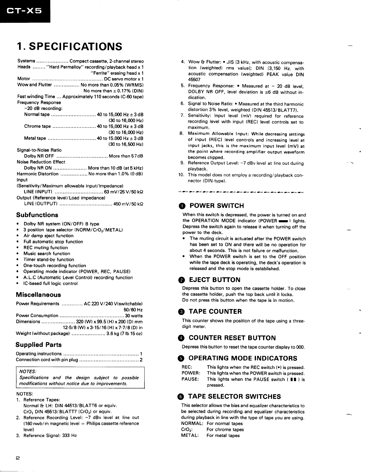
6.
CIRCUIT DESCRIPTIONS
6.1 OUTLINE
OF MAIN
STAGE
PlaybackEqualizer
Circuit
TheEQamplifieremploys
2-stagedirect-coupled
amplifier, ild the NFB circuit is designed for
playback equalizationwith normal (NORM) tapes.
For playback equalization with chrome (CrO2
)
and metal (METAL) tapes, the transistor switch
is turned on to incorporate the RC network in the
output circuit of the EQ amplifier.
Dolby Noise
Reduction
System
The CT-X5 features the B-type Dolby noise
reduction system (where the S/N ratio is improved
by up to 10dB above SkHz) incorporated in a
Dolby IC (HA1L226).
Recording
Amplifier
The recording amplifier uses a single transistor
and has a high frequency peaking circuit in the
emitter, and a trap in the output circuit to prevent
leakage of the recording bias signal. The peaking
response of the high frequency equalization cir-
cuit can be changed to give three different re-
sponses
by the TAPE SELECT switchesfor dif-
ferent types of tape (NORM, CrO, and METAL).
Further, during playback, both the input and
output circuits of this amplifier a^re
grounded.
BiasOscillator
This push-pull oscillator circuit supplies the
eraseheadwith the erase
current, and the recording
head with the recording bias current. The dif-
ferent recording bias levelsfor the different types
of tape (NORM, CrO2 and METAL) are switched
by changing the oscillator power supply voltage
which in turn varies
the oscillating power.
6.2 CONTROLCIRCUIT
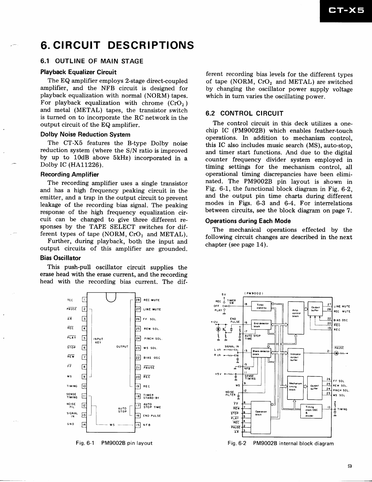
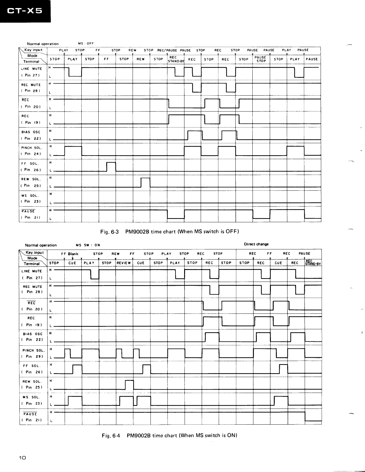
The control circuit in this deck utilizes a one-
chip IC (PM9002B) which enablesfeather-touch
operations. In addition to mechanism control,
this IC alsoincludesmusic search
(MS),auto-stop,
and timer start functions. And due to the digital
counter frequency divider system employed in
timing settings for the mechanism control, all
operational timing discrepancies
have been elimi-
nated. The PM9002B pin layout is shown in
Fig. 6-1, the functional block diagramin Fig. 6-2,
and the output pin time charts during different
modes in Figs. 6-3 and 6-4. For interrelations
between circuits, seethe block diagram on page
7.
Operations
duringEachMode
The mechanical operations effected by the
following circuit changes
are describedin the next
chapter(seepage
14).
"..J
''"t'
vcc
pltrse
a-E-
OFF O
erav
f
l,
ENO
PULSE
REC
PLAY
srop
n-e
w
M5
TIM
ING
SENSE
TIM
ING
NOISE
FIL
SIGNAL
IN
GND
NOISE
FILTERx
itw-
si6F
FrIV
TEC
FAUSE
AR
LTimanO
clck OSC
&
divrdcr
Fig.6-2 PM9002B
internal
block
diagram
Fig.6-1 PM9002B
pin
layout