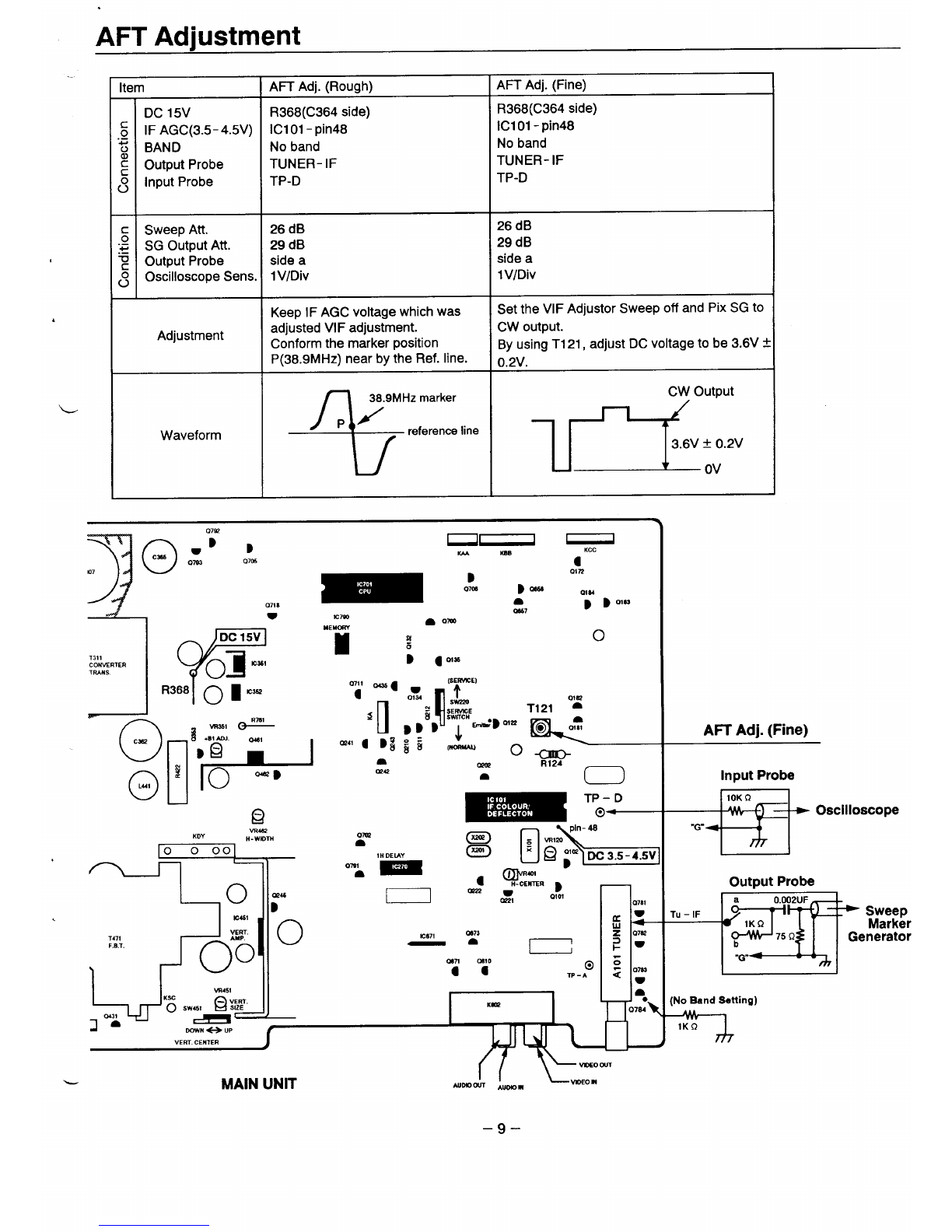
logo
Brands
  1. Home
  2. •
  3. Brands
  4. •
  5. Sanyo
  6. •
  7. TV
  8. •
  9. Sanyo C29ZK80 User manual

Sanyo C29ZK80 User manual

Other manuals for C29ZK80

1

Other Sanyo TV manuals

Sanyo DP32640 - 31.5" Diagonal LCD HDTV 720p User manual

Sanyo

Sanyo DP32640 - 31.5" Diagonal LCD HDTV 720p User manual

Sanyo ce29ef1 User manual

Sanyo

Sanyo ce29ef1 User manual

Sanyo CE32WN4 User manual

Sanyo

Sanyo CE32WN4 User manual

Sanyo CZP3024 User manual

Sanyo

Sanyo CZP3024 User manual

Sanyo CTP3618N User manual

Sanyo

Sanyo CTP3618N User manual

Sanyo CE27LD6-B User manual

Sanyo

Sanyo CE27LD6-B User manual

Sanyo CE25DN5-C User manual

Sanyo

Sanyo CE25DN5-C User manual

Sanyo AVM-3660G User manual

Sanyo

Sanyo AVM-3660G User manual

Sanyo DS25500 User manual

Sanyo

Sanyo DS25500 User manual

Sanyo C29ZK80 User manual

Sanyo

Sanyo C29ZK80 User manual

Sanyo CZP3359TX User manual

Sanyo

Sanyo CZP3359TX User manual

Sanyo C29LF34 User manual

Sanyo

Sanyo C29LF34 User manual

Sanyo CP21G1(C) User manual

Sanyo

Sanyo CP21G1(C) User manual

Sanyo CE28SN3-C User manual

Sanyo

Sanyo CE28SN3-C User manual

Sanyo CE21KF8R User manual

Sanyo

Sanyo CE21KF8R User manual

Sanyo DS25520 User manual

Sanyo

Sanyo DS25520 User manual

Sanyo DS19310 User manual

Sanyo

Sanyo DS19310 User manual

Sanyo FVM4612 User manual

Sanyo

Sanyo FVM4612 User manual

Sanyo CM21SP81 User manual

Sanyo

Sanyo CM21SP81 User manual

Sanyo CE25DN7-C User manual

Sanyo

Sanyo CE25DN7-C User manual

Sanyo LCD-39XZ12F User manual

Sanyo

Sanyo LCD-39XZ12F User manual

Sanyo CP29EF1K User manual

Sanyo

Sanyo CP29EF1K User manual

Sanyo C29AK86 User manual

Sanyo

Sanyo C29AK86 User manual

Sanyo DS27431 User manual

Sanyo

Sanyo DS27431 User manual

Popular TV manuals by other brands

Philips 32PFL7403D null

Philips

Philips 32PFL7403D null

Philips 19PFL3403D null

Philips

Philips 19PFL3403D null

Philips 19PFL5403D null

Philips

Philips 19PFL5403D null

Philips 32PFL7605C null

Philips

Philips 32PFL7605C null

Philips 32PFL7603D - annexe 1 null

Philips

Philips 32PFL7603D - annexe 1 null

Haier HS-2190 null

Haier

Haier HS-2190 null

Philips 19PFL3404D null

Philips

Philips 19PFL3404D null

Toshiba 27A10 owner's manual

Toshiba

Toshiba 27A10 owner's manual

Philips 42PF9630A/37 user manual

Philips

Philips 42PF9630A/37 user manual

Hitachi 32FX48B operating guide

Hitachi

Hitachi 32FX48B operating guide

DAEWOO ELECTRONICS DTQ-14V1FC Service manual

DAEWOO ELECTRONICS

DAEWOO ELECTRONICS DTQ-14V1FC Service manual

Changhong Electric uhd55b6000is Operation manual

Changhong Electric

Changhong Electric uhd55b6000is Operation manual

Philips Matchline 21CE7551 operating instructions

Philips

Philips Matchline 21CE7551 operating instructions

Panasonic Genus TX-G10 operating instructions

Panasonic

Panasonic Genus TX-G10 operating instructions

Toshiba 19A20 Service manual

Toshiba

Toshiba 19A20 Service manual

Philips 25PT4523-16 manual

Philips

Philips 25PT4523-16 manual

Sony XBR-100Z9D reference guide

Sony

Sony XBR-100Z9D reference guide

Philips PR0930X3 owner's manual

Philips

Philips PR0930X3 owner's manual

https://manuals.online logo
https://manuals.online logoBrands
  • About & Mission
  • Contact us
  • Privacy Policy
  • Terms and Conditions

Copyright 2026 Manuals.Online. All Rights Reserved.

.SA\/YO
SERVICE MANUAL Colour Television
FILE NO.
Model No. C29ZK80
(New Zealand)
Service Ref. No. C29ZK80- 00
(1) r
.Specifications
LPower Source .................... AC 220 – 240 Volts, 50Hz.
Colour System ................... PAL
(AV INPUT: PAL/NTSC/NTSC4.43)
Television System ............. B/G
Channel Coverage, ............ VHF 1 – 11
UHF: 21 – 69
cVideo IF ............................. 38.9MHz
*Sound IF ............................ 33.4 MHz
Aerial Input Impedance ...... 75 Q
Ext. Terminals, ...................AV Inputs
Video inputs: Phono jack x 1
Audio inputs: Phono jack x 1
AV Outputs
Video outputs: Phono jack x 1
Audio outputs: Phono jack x 1
Headphone Jack: Mini. Jack x 1
Sound Output (Music) ........ 5W
Dimensions.., ..................... 700(W)X601 .5( H)x495(D)mm
Weight(approx.) ................. 39.1 Kg
Product Code: 111324409
Original Version
Chassis Series: AAl -A
Give complete “SERVICE REF. No.” for parts
order or servicing. It is shown on the rating plate
at the cabinet back of the unit.
This T.V. receiver will not work properly in
foreign countries where the television trans -
mission system and power source differ from the
design specifications. Refer to the specification
table.
Refer to “T1520004” Training Manual
for this model.
LSpedfjcations subject to change without notice. REFERENCE NO. SM 520177
E8DK
TEXT DECODER
1- -------------.-7 0
0
x
l~lvcc ].Digital Control
...... II
........................
;Rout 49 YELK
~Gout ~BRout
~Bout IrGout
OSD a
u~Bout
II InIm
nn
1n
-------- ------ ---
I II Iclol --—- 1I
~’N a-
(TDA4665)
lH Delay
~
d= J
\
B8: 5V(TEXT) tHV
IG=EE=3-I I
5’
B6:12V
ICB71
I
N
IIT471FBT I
R
‘Y
20
27
Q431 Q432
H-Drive& H- C)lJT ~
Tl--
=!I ~
r?
TV/AV SW
1
=+
r-. Video out
Audio out
,Videoln .‘* ~Deflection
4Yoke
H
~3
Icllol v
“3
[AN5265)
REAR
L
v@ Audio In
A@ I-----
.........- .....................,E
:10
~SIFSwitching :B7:8V
(4.5/5.5
o/6.O/6.5MHz :
!Filter
.....................
Audio AMP.
ACna.ka,
m%“~..u,.”,
m.-.
T501
&
POWER T311
TRANS CONVERTER
------ IC351
‘-----------: TRANS. r------------------------ ~I=fi
Acti
‘erciruitF~:ZE,,............................
ISpeaker
dSP2
,.,.,, ,..-,—,,,gh); ln=u’3 !_-----: ””------: ””----”””l
,*V ,muu,”,
c
B6:12V (Mare Lowl ):
‘-” ‘--’’’--T) ~...........................
IC352
REG. ..........................
13
,1 IB7:6V (Main Low2) !
............................ .......................... ●
(
.
Block Diagram (Formulti-standardModel)
--
........................................
...”
El-d+
4S1
(DI06)
,.. . .*
L
!,
L.. ...!
NTSC
Band Limited
*
101 (TDA8361
Vin
:in
-rvOut
SECAM
REF.
;IF in
CHROMA ID
TV ID.
(TIME BASE)
$---.. ---.: S2 5.5 MHz Trap
iP=- 4.5 MHz Trap
r
—
32
—
26
r$
—
34 35
m@-”””
,L-....,......
......
6.5 MHz Filter +%
S11
(Ql 56)
......
6.OMHZ Filter
-~% Slo
(Q155)
..----
5.5 MHz Filter ~%
S9
(Q154)
......
4.5 MHz Filter \
SIF Filter P(Q153)
~y—+
S3 Sound Cam.er Trap
D121) 5.516.016.5MHz Trap
+----p:INV IC2B0
(SECAM)
(Q157) ,,—1
i’ ............
................................................
IC701 (CPU) \
18 SECAM ?“--~
+CID.
-’s TV ID. 4.5 MHZ 39-.. --.---. -.--..+
5.5 MHZ 36------------ i
42 4.43 MHZ
. .. . .
--4? 3.58 MHz
V-SYNC.
2
V-SYNC. Pulse
(for O.S. D.)
...................................
. .
;;
:::
:::
:::
:::
........-................................ ::
::
:,
..............................................
..................................................J
–3–
Circuit Description
1. POWER SUPPLY
The power supply circuit of the Ml -Achassis is
comprises aprimary rectifier smoothing circuit, an
oscillation circuit, acontrol circuit and an output rectifier
circuit.
The AC input voltage is rectified at the double or full-wave
rectifier smoothing circuit, and an unstable DC voltage is
generated at both terminals of the smoothing capacitor
C307. This voltage is supplied to the oscillation circuit,
which is composed of ablocking oscillator circuit that
switches the switching transistor Q313 ON and OFF.
Asquare-wave oscillation is generated in the input
winding according to operation of the control circuit. A
quare-wave with amplitude dependent on the turns ratio of
the input and output windings is obtained in the output
winding. This is rectified in the output rectifier circuit, and
the desired DC voltage is produced.
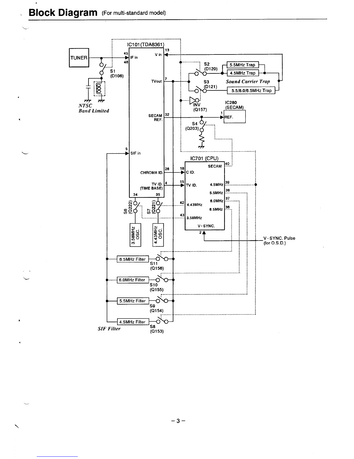
2. IF& DEFLECTION (TDA8361/8362)
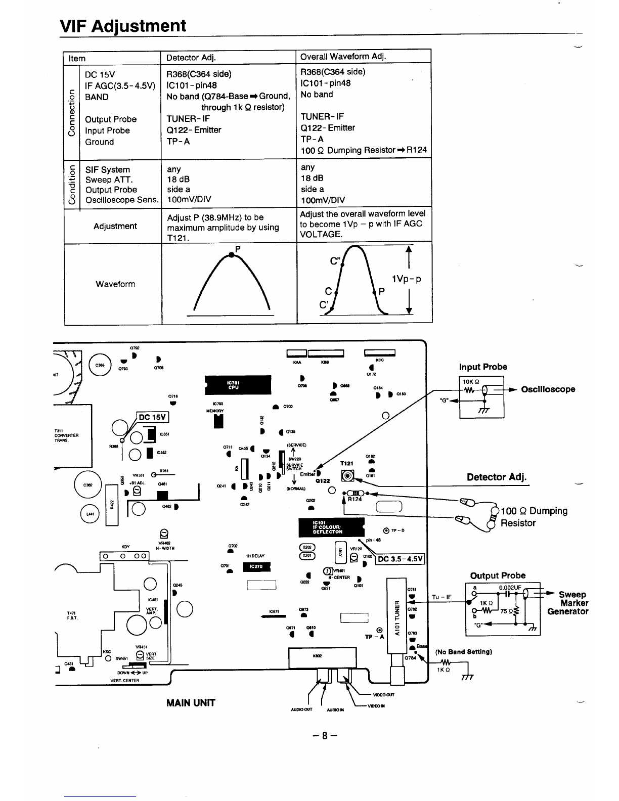
The IF output signal from the tuner passes through the
SAW filter, and it is input to pins 45 and 46ofIC101.
Within the IC, the IF signal passes through the IF
amplifier, video detection and video amplifier circuits, and
~is outputted from pin 7as acomposite video signal. In the
monaural model, this composite video signal passes
through the 5.5 MHz(B/G) /6.OMHZ(I) /6.5 MHz(D/K) /
4.5 MHz(M) sound bandpass filtering circuit, and it is
inputted into pin5 of IC101. In the stereo model, the SIF
signal is supplied from pin 14 of IC181 <TDA2546A> to
pin 5of IC101 through the sound bandpass circuit for
modulation of the main carrier. In the IC101, this sound IF
signal passes through the SIF amplifier, FM detector,
external audio switch and audio output circuit, and it is
then outputted from pin 50 as audio drive signal (Monaural
model). In the stereo model, the main audio signal is fed
from pinl to the stereo controller ICI 103(MC44131 PB).
The video signals applied to pins 13 or 15 are separated
into vertical -and horizontal -sync. signals respectively by
the sync. separator in the IC.
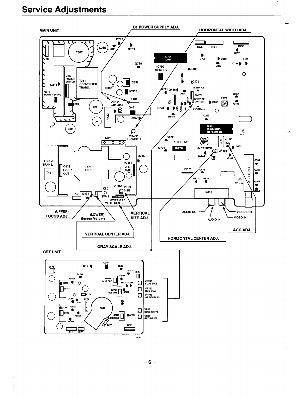
The horizontal oscillator requires no external components
and is fully integrated. This oscillator is always running
when the start -pin 36 is supplied with 8V, and the
horizontal drive signal is outputted from pin 37. VR401 is
used for horizontal centring adjustment.
The separated vertical sync. signal from the sync.
separation circuit passes through the vertical -separation
circuit, and is applied to trigger divider circuit.
The horizontal oscillation pulse and vertical sync. pulse
are monitored by the trigger divider circuit to select either
the 50Hz or 60Hz system, and automatically adjust the
vertical amplitude.
The output signal from the trigger divider triggers the
vertical oscillator circuit whose external timing
components consist of R402, C401 to pin 42, and the
w
vertical ramp signal is outputted from pin 43. VR451 is for
controlling the amount of AC feedback applied to pin 41
for adjustment of the vertical amplitude.
3. VIDEO CHROMA (TDA8361/8362)
The composite video signal output from the pin 7ofIC101,
passes through Q122, and the sound traps Xl 24, Xl 25,
X126, X127 to reject the sound carrier components, is
then supplied to pin 13 through the equalizing circuit
consisting of Q135, Q132 and Q1 34. The external video
signal from SCART or other AV terminals is supplied to
pin 15.
The video signal input to pin 13 or pin 15 is separated into -
luminance (Y) signal and chroma signal in IC101. These
pins are also common to the H/V- sync. separation circuit
input already described.
The peaking of Ysignal is adjusted by DC voltage on pin _
14.(’’SHARPNESS” control)
The chroma signal is divided into R-Y and B-Y chroma
signals, which are demodulated and output from pin 30 (R
-Y) and pin 31 (B -Y). These chroma signals pass
through the 1Hdelay line circuit (IC270), and are re -
inputted at pin 29 (R-Y) and pin 28 (B-Y). These R-Y/B-
Ysignals pass through the RGB matrix circuit and the
RGB selector circuit of IC101. The internal RGB signals
are generated in the RGB matrix circuit and the RGB
selector, consisting of linear amplifiers, clamps and
selects either the internal RGB signals or the external
RGB signals input from pin 22 (R) ,pin 23 (G), pin 24 (B).
Selection is controlled by the voltage at the RGB switch
control (pin 21) and mixed RGB modes are possible since
the RGB switching is fast.
The RGB switch also functions as afast blanking pin by
blanking the RGB output stages; here internal and
external RGB signals are overruled.
The RGB signals for the on -screen display are
superimposed onto the selected RGB signals at the base
of transistors Q21 O,Q211 and Q212 respectively.
The saturation of colour gain is controlled by the DC
voltage of pin 26. (“COLOUR” control)
The contrast control voltage present at pin 25, controls the
RGB signal gain, and the brightness control voltage
present at pin 17, controls DC level of RGB signals.
The RGB signals are finally buffered before being
presented to the RGB output pins [pin 20 (R), pin 19 (G),
pin 18 (B)].
–4–
.
Circuit Description
.- 4. AUDIO OUTPUT
4-1 (AN5265)-Monaural model
The audio signal output from pin 50ofIC101 is inputted to
pin 2of IC1101 and passes through the pre -amplifier
circuit and the drive circuit into the audio amplifier. The
audio amplifier is the SEPP (Single -Ended Push Pull)
type and the output from pin 8drives the speaker directly.
4-2 (TDA7263M)-Stereo model
The audio signals output from pins 17 and 18 of
.ICI 103(MC44131 PB) are inputted to pins 1(Left) and
5( Right) of IC1 102 and passes through the pre -amplifier
circuit and drive circuit, after which it is input to the audio
.amplifier. The audio amplifier is the SEPP (single- ended,
push -pull) OTL type and the outputs from pins 8( Right)
and 10(Left) drive the speakers directly.
5. VERTICAL OUTPUT
L. An LA7833 is used for the vertical output circuit in this
chassis. The vertical ramp signal from pin 43 of IC101 is
inputted to pin 4of IC451. This ramp drives IC451, and
vertical scanning is performed. In the first half of scanning
adeflecting current is outputted from pin 2 and passes
through the following path:
VCC(B4) +D451 +pin 3+pin 2+DY +C461 +
VR451 /R459.
An electric charge is then stored in C461. In the last half of
scanning the current path is:
C461 +DY +pin 2+pin 1+VR451/R459 +C461
In this way, an increasing sawtooth waveform current
flows directly to the DY to perform electron beam
deflection. During the first half of the blanking period the
vertical ramp signal suddenly turns OFF. Since there is no
longer any current flowing into the DY, the magnetic field
collapses causing an induced current to flow as follows:
DY+ pin 2+ pin 1+VR451/R459+C461 +DY
LOnce the magnetic field in DY has dissipated, the current
path becomes:
Vcc+ pin 6+ pin 7+ C452+ pin 3+ pin 2+ DY+ C461
+VR451 /R459
and when the prescribed current value is reached, the
vertical drive ramp signal turns ON.
,This completes one cycle.
6. HORIZONTAL OUTPUT
The horizontal oscillation signal is outputted from pin 37 of
IC101 and used to switch the drive transistor Q431. This
switching signal is current amplified by the drive
transformer T431 and drives the output transistor Q432.
When Q432 turns ON, an increasing current flows directly
to the DY through
C441/C442 +L441/R441 +DY +Q432- C+Q432- E
and the deflection occurs during the last half of the
scanning period. When Q432 turns OFF, the magnetic
w
field stored in the DY up to that point causes aresonant
current to flow into the capacitors C420 and C423 and
charges them.
The current stored in C420 and C423 then flows back to
the DY causing an opposite magnetic field to be stored in
the DY. This field then collapses increasing acurrent
which switches the dumper diode in Q432 ON. The
resonance state is completed, and an increasing current
then flows again directly to the DY through the dumper
diode.
By this means, the deflection in the first half of the
scanning period is performed. When Q432 turns ON at the
end of the first half of the scanning period, the deflection
during the last half is begun, thus completing one cycle.
In the PCC circuit consisting of Q461 and Q462, the
parabola signal supplied from the vertical circuit is added
at the horizontal output stage and pincushion
compensation is performed by varying the DC bias.
Further, the ABL voltage is fedback to the base of Q462 to
compensate for width variations due to variations in the
beam current.
–5–
Service Adjustments
MAINUNIT El POWER SUPPLY ADJ. HORIZONTAL WIDTH ADJ.
D
0705
0718
w7B0172
Oms Dosss 01s2
a
IC790 om oD
MEMORY ao700
kxJ==’-
0313
POWER
SWITCH T311
CONVERTER (OJ
00 IC351
TRANS.
D.316 ~‘v>
,-...— +Bl AOJ. ~.-.
o
/----- ..
T171
k%’%
o
PI
o
L4S2
+
U40 1
0462 D
/
[
0432
HORIZ.
OUT
H-ORIVE
TRANS.
❑
T431
o‘IL-J-”I
IC451 w
T471 VERT.
F.B.T, AMP.
00 0
VR451 ~R~,
KSC
KB 0431 0QgE
—. CWA%I ~
/ \
7’
IC871 0s73
a[—] \
0s71 0810
Ca @
TP-A
K802
I
AUOIO OUT
AUOIO IN
L
a+ YJ!W!N-l
HORIZONTAL CENTER ADJ.
VERTICAL CENTER ADJ.
GRAY SCALE ADJ.
.
CRT UNIT 1
VR7S2
BLUE BIAS
VR7S2
RED BIAS
VR772
QREEN BIAS
VR7S1
BLUE ORIVE
VR7St
RED DRIVE
–6–
Service Adjustments
SAFETY PRECAUTIONS :An isolation transformer should be connected in the power line between the receiver and the AC
--- line before any service is performed on the receiver.
X-RADIATION PRECAUTION The primary source of X-RADIATION in television receiver is the picture tube. The picture
tube is specially constructed to limit X-RADIATION emission. For continued X-RADIATION protection, the replacement tube must
be the same type as the original including suffix letter. Excessive high voltage may produce potentially hazardous X-RADIATION.
To avoid such hazards, the high voltage must be maintain within specified limit. Refer to this service manual for specific high
voltage limits. If high voltage exceeds specified limits, take necessary corrective action. Carefully follow the instructions for +B1 volt
power supply adjustment, and high voltage check to maintain the high voltage within the specified limits.
s
NOTE; Do not attempt this adjustment with weak signal.
(1) Tune the receiver to most clearest (or strongest) VHF
.station in your area. Set the brightness and contrast
controls to maximum. Set the colour control to minimum. 0
(2) Set AGC (VRl 20) control to mid- range.
(3) Turn AGC control in direction which causes snow to appear,
then in the omosite direction until the snow iust disarmears.
.
“L
(1) Connect DC meter to R761 (VR351 side) and the ground.
Set the +Bl adjustment control (VR351 )to mid-range.
(2) Set the brightness and contrast to normal,
Tune the receiver to an active channel and synchronized
picture.
(3) Adjust +Bl adjustment control(VR351 )for 140 *0.5 volt
DC.
(1) Receive the monochrome circular pattern.
(2) Set the brightness and contrast to normal.
(3) Adjust VR401 for optimum horizontal center position.
Horizontal center
(1) Receive the monochrome circular pattern,
(2) Set the brightness and contrast to normal.
(3) Vertical centering can be adjusted by switching SW451.
:Eili3iF
Vertical center
(1) Receive the monochrome circular pattern.
(2) Set the brightness and contrast to normal.
(3) Vertical size can be adjusted by using VR451.
rtical size
(1) Receive the monochrome circular pattern.
(2) Set the brightness to normal and contrast to maximum.
(3) Adjust the focus control on the F.B.T forthe best focus on
the screen center.
(1) Receiver the monochrome circular pattern.
(2) Set the brightness and the contrast to maximum.
(3) Set the drive volume (VR761 and VR781 )at their
mechanical center.
(4) Set the bias volume (VR762, VR772 and VR782) to
minimum. (fully counter clockwise).
(5) Set the service switch (SW220) to the service side.
(6) Turn the screen volume on the FBT to obtain just visible
one coloured line.
(7) Adjust each bias volume (VR782- blue, VR772- green and
VR762- red) alternately until adim white line produced.
(8) Set the service switch (SW220) to the normal side.
(9) Adjust the drive volume (VR781 -blue and VR761 -red)
alternately to produce normal black and white picture.
(1 O)Check for proper grey scale tracking at all brightness
levels.
NOTE :If the grey scale adjustment is made after picturetube
replacement, check high voltage and sub -brightness
adjustment,
(1) Receive the monochrom circular pattern.
(2) Set the brightness and contrast to normal.
(3) If the picture is too wide or narrow, adjust the horizontal
width using VR462.
NOTE: The horiz. width adjustment affects the high voltage.
Therefore, recheck the high voltage.
(1) Connect ahigh voltage probe to anode lead of the picture
tube.
(2) Receive the monochrom circular pattern.
(3) Set the brightness and contrast to maximum.
(4) The high voltage must be between 28-30 t1XV.
NOTE: If the picture tube is replaced, check the high voltage.
–7–
,
VIF Adjustment —
Overall Waveform Adj.
Item Detector Adj.
R368(C364 side)
ICI 01- pin48
No band (Q784-Base =+ Ground,
through 1k Qresistor)
TUNER- IF
Q1 22-Emitter
TP-A
—
c
o
.-
G
al
c
c
8
.c
0
.-
.1-
.-
-u
c
8
—
R368(C364 side)
IC101 -pin48
No band
DC 15V
IF AGC(3.5- 4.5V)
BAND
Output Probe
Input Probe
Ground
TUNER- IF
Q1 22- Emitter
TP-A
100 QDumping Resistor* RI 24
any
18dB
side a
10OmV/DIV
any
18dB
side a
10OmV/DIV
Adjust the overall waveform level
to become lVp –pwith IF AGC
VOLTAGE.
SIF System
Sweep ATT.
Output Probe
Oscilloscope Sens
Adjustment Adjust P(38.9MHz) to be
maximum amplitude by using
T121 .P
AL
ct
Ivp-p
cP
c’
Waveform
Input Probe
+!a-
FDC 15V
1311
CONWRTER Oa Kxl$l
TRAMS
‘w on””
Detector Adj.
-a 100 QDumping
Resistor
Om
nlH DELAY (invRWl-
aOutput Probe%-CENTER
wB
Ix-21 08QI
I I YE!!I
1I
mm 0s10
a4
!jj4!+KbL&JJ ,il. 1
DOWN eUP
vERT. CENTER
(No Band Belting)
7lKQ
MAIN UNIT ( [ c;:”
AUDlOWl AUDIO N
–8–
.-
,
L
.
AFT Adjustment
Item AFT Adj. (Rough) AFT Adj. (Fine)
DC 15V R368(C364 side) R368(C364 side)
,: IF AGC(3.5-4.5V) IC101 -pin48 ICI 01- pin48
~BAND No band No band
:Output Probe TUNER-IF TUNER- IF
;Input Probe TP-D TP-D
cSweep Att. 26 dB 26 dB
:; SG Output Att. 29 dB 29 dB
~Output Probe side aside a
;Oscilloscope Sens. lV/Div 1V/Div
Keep IF AGC voltage which was Set the VIF Adjustor Sweep off and Pix SG to
Adjustment adjusted VI Fadjustment. Cw output.
Conform the marker position By using T1 21, adjust DC voltage to be 3.6V *
P(38.9MHz) nearby the Ref. line. 0.2V.
Waveform *,Iline ,~+;v
—
1-
0718
PDC 15V
1311
CC+WERTER 01 NX61
WwLs
‘oii
o
L4!
u(1
—
J“- TP– D
@—
wlw
KDY ,.-.. —
H- WIDTH
n~pln-48
IIw
am &
1471
<0\
yy
F.B.T. oICI171‘~
oI
I
cm
)
0510
a a
Am Adj. (Fine)
Input Probe
+!!5
Output Probe
w“
(No Band Setting)
m
&MAIN UNIT II
AUDIDOUT-~ VIDEOm
–9–
PURITY AND CONVERGENCE ADJUSTMENT
CAUTION:The Convergence and Purity adjustments have been made at the factory. Readjustment should be
made only after picture tube or deflection yoke replacement, following the steps below.
PURITY ADJUSTMENT
1.Demagnetize the picture tube and receiver using an external
degaussing coil. When replacing picture tube or deflection
yoke, mount deflection yoke and purity -convergence
magnets assembly properly, see figures 1and 4.
2.Turn Red and Blue guns off and provide only Green raster.
Rotate Screen control to fully counterclockwise. Rotate Red
and Blue Bias controls fully counterclockwise. Slowly rotate
Green Bias control clockwise to produce Green raster.
3. Loosen the screw holding the Deflection Yoke and remove
the 3Rubber Wedges, and slide the Deflection Yoke fully
frontward.
4. Rotate and spread the Tabs of the two Purity Magnets to
center the vertical green belt in the picture screen. The Purity
Magnets are also adjusted to obtain vertical centering of the
raster.
5. SIOWIY slide the Deflection Yoke backward until auniform
green screen is obtained.
6. Check the purity of the red and blue screens for uniformity,
turn off other colours to check this (use bias controls).
Readjust the yoke position if necessary until all screens are
n, are
vu, -.
7. Adjust each Bias control and screen control to obtain white
raster. Refer to Gray Scale Adjustment. If part of the picture
screen is coloured, adjust the Deflection Yoke position
forward or backward slightly,
8. Tighten the mounting screw of the Deflection Yoke. Adjust
Convergence next.
CENTER CONVERGENCE ADJUSTMENT
1. Use adot crosshatch pattern signal.
2. Turn Red and Blue guns on and turn off Green gun. Adjust
the angle between the Tabs of the Four Pole Magnet 1and
2,and superimpose the Red and Blue vertical lines in the
center area of the picture screen. Refer to figure 2.
3. Keeping the mutual angle of the Tabs of the Four Pole
Magnet turn them together to superimpose the Blue and Red
horizontal lines in the center area of the picture screen. Refer
to figure 2.
4. Turn Green gun on and adjust Six Pole Magnet 3and 4s that
the Green line superimposed on the Red/Blue lines.
This is the same procedure used in steps 2and 3.
Refer to figure 3.
OUTER AREA CONVERGENCE ADJUSTMENT
Slightly loosen the screw holding the Deflection Yoke. Adjust
the Deflection Yoke to converge the detail in the outer area (left
side and right side) of the picture screen by orbital movement of
the front of the Yoke, then secure the Deflection Yoke in
appropriate position by putting the wedges as illustrated.
Tighten screw holding the Deflection Yoke.
Figure- 1. PURITY AND CONVERGENCE MAGNETS
DEFLECTION YOKE
FOUR- POLE
MAGNET TABS SIX- POLE
rx A
MAGNET TABS
Figure- 4. ADJUSTMENT DEFLECTION YOKE
Adjust tabs angle to superimpose
blue and red vertical line Adjust tabs angle to superimpose
red/blue and green vertical line
Figure- 2BLUE AND RED LINE MOVEMENT IFigure- 3BLUE/RED AND GREEN LINE MOVEMENT
.x
.-
–lo–