-9-
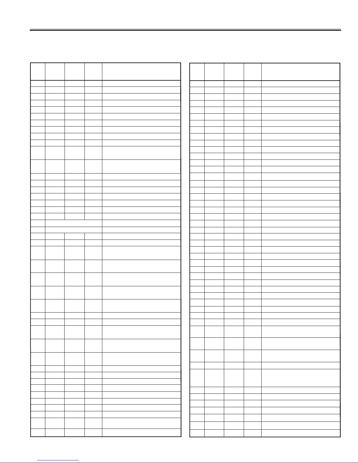
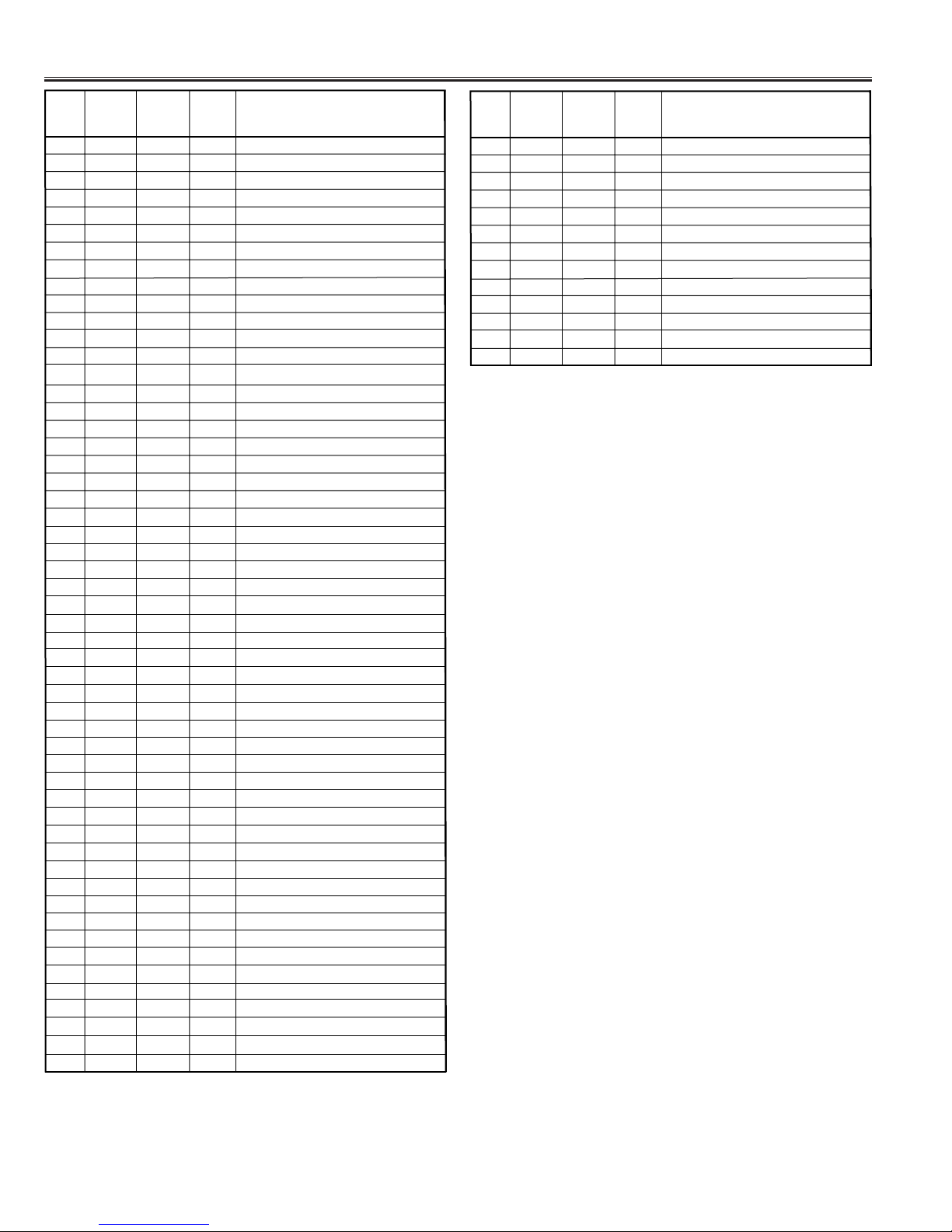
Service mode adjustments table in CPU ROM
NO. ITEM DATA
RANGE
INITIAL
SETUP
DATA
DESCRIPTION
01
02
03
04
05
06
07
08
09
10
11
12
13
14
15
16
17
18
19
20
RF AGC Adj.RF AGC 00~63 22
H-Phase (H-Centering) Adj. (50Hz)H-PHA 00~31 5
V-Position (V-Centering) Adj. (50Hz) Fixed.
V-POS 00~63 40
V-Size Adj. (50Hz)V-SIZ 00~127 42
V-S Correction (50Hz)
V-SCO 00~31 15
V-Linearity Adj. (50Hz)
V-LIN 00~31 10
H-Centering Adj. (60Hz)H-P60 -16~+15 +5
V-Size Adj. (60Hz)
V-S60 -64~+32 0
OSD H-Position Adj.
OSDHP 00~255 29
OSD Contrast Adj.OSDC 00~127 40
Correction of the V-size accompanying
brightness change.
V-SCP 00~07 7
Correction of the H-size accompanying
brightness change.
H-SCP 00~07 7
Sub Bias Adj.SBIAS 00~127 105
Red Bias Adj.RBIAS 00~255 0
Green Bias Adj.GBIAS 00~255 46
Blue Bias Adj.BBIAS 00~255 29
Red Drive Adj.RDRIV 00~127 76
Green Drive Adj.GDRIV 00~15 8
Blue Drive Adj.BDRIV 00~127 75
1-LINE APPEAR
21 DRV White Balance Adj.
22 B-YD 00~15 9
B-Y DC level Adj.. Colour compensation (PAL)
23 R-YD 00~15 9
R-Y DC level Adj.. Colour compensation (PAL)
24 B-YDN -16~+15 0NTSC B-Y DC level Adj.
(Difference value over PAL.)
25 R-YDN 0NTSC R-Y DC level Adj.
(Difference value over PAL.)
26 SBDC -8 SECAM B-Y DC level Adj.
(Difference value over PAL.)
27 SRDC -5 SECAM R-Y DC level Adj.
(Difference value over PAL.)
28 G-YA 0,1 0G-Y angle Adj. (The reproducibility of
a colour is changed.)
29 RBGB 00~15 8
R-Y, B-Y Gain Blance Adj. (Do not change.)
30 RBAG 00~15 8R-Y, B-Y Angle Adj. (Do not change.)
31 G-YAN 0,1 0NTSC G-Y Angle Adj.
(Difference value over PAL.)
32 RBGBN 0NTSC R-Y, B-Y Gain Balance Adj.
(Difference value over PAL.)
33 RBAGN 0NTSC G-Y, B-Y Angle Adj.
(Difference value over PAL)
34 COGV 00~03 0Coring Adj.
35 BLKS 00~03 3Setting of Black stretch start.
36 BLKG 00~03 3Setting of Black stretch gain.
37 BRTA 0,1 0On and off of ABL.
38 BRST 0,1 0Setting of ABL.
39 BRTH 00~07 0Setting of ABL.
(Do not change)
40
41
42
43
White peak limitter.WPL 00~03 2
Y Gamma setting.YGAM 00~03 0
Switching of Pre-shoot and Over shoot
in AV mode.
PORW 0,1 0
Pre-shoot/Over shoot Adj. in AV mode.
PORS 00~03 2
-16~+15
-16~+15
-16~+15
-16~+15
-16~+15
NO. ITEM DATA
RANGE
INITIAL
SETUP
DATA
DESCRIPTION
44
45
46
47
48
49
50
51
52
53
54
55
56
57
58
59
60
63
64
65
RF Coring Gain Adj.RFCO 00~03 0
Switching of RF Pre-shoot and Over shoot.
PORWN 0,1 0
RF Pre-shoot/Over shoot Adj.
PORSN 00~03 0
RF Tint Adj.TINT -16~+15 0
NTSC 4.43 Tint Adj.
TINT 443 -16~+15 -12
RF Sharpness Adj.
SHRF -32~+31 0
OSD TEXT Contrast.TEXTC -
128
~+
127
0
VOLUM 127
0
0
1
16
0,1
0
1
00~255
1
34
00~63
136
0,1 0
00~07
66
67
0
68
0
69
0
70
1
71
0
72
0
73
1
74
3
75
64
76
0
77
0
78
5
79
1
80
0
81
82
1
83
112
84
64
0
0
1
0
Volume Control Adj.
00~255
De emphasis TC.DEEM 00~01
VIF System Switch.VIFSW 00~03
SIF System Switch.SIFSW 00~03
Video Level Adj.V-LVL 00~07 4
FM Level Adj.FMLVL 00~31
IF Test
IF-TE 0,1
IF Test-1
IF-T1
IF-T2
IF-T3
61 H-FRQ Correction of Horizontal Frequency.
62 FBTS
Switching of H-blanking and Flyback Pulse.
COOP
00~07
Setting of Colour Killer Level.
HBLKL H-Blanking Control. (Left)
HBLKR 00~07 H-Blanking Control. (Right)
AFCRF 0,1 RF AFC Gain & Gate Adj.
VSURF 0,1 RF V-Sync. Separation Adj.
CDMRF 00~07 RF V-Countdown Circuit Adj.
AFCAV 0,1 AV AFC Gain & Gate Adj.
VSUAV 0,1 AV V-Sync. Separation Adj.
CDMAV 00~07 AV V-Countdown Circuit Adj.
HLVDRF 0,1 H Lock, V Detect RF mode
HLVDAV 0,1
VCO-SW 0,1 C-VCO Adj. Switch.
VCO-ADJ
00~03 C-VCO Adj.
CROSS-BW
00~03 Pattern Output.
AVNCON 00~127
Contrast Adj. of the blue back in AV mode.
AVNBRI 00~127
Brightness Adj. of the blue back in AV mode.
IF Test-2
POMT 00~127 Power Mute Time Adj.
CHMT 00~31 Channel Change Mute time Agj.
SYST 00~15 Selection of the number of times of
a Colour system judgment.
S-STE 0,1 Stereo/Mono Option.
0
=MONO, 1=AV STEREO
VOLTBL Selection of the change characteristic
of volume.
818/828 Metal Option
302 R02 00~255 CPU Debug Date.
303 R03 00~255 CPU Debug Date.
301 R01 00~255 CPU Debug Date.
300 R00 00~255 CPU Debug Date.
CHIP818
0,1
IF Test-3
7
7
3
1H Lock, V Detect AV mode
64
25
10
CPU Debug Date.
CPU Debug Date.
CPU Debug Date.
0
00~255
00~255
00~255
304
305
306
R04
R05
R06
0~3
0,1
Service Adjustments with Replacing Memory IC(IC802)
Following table shows the initial values which have been stored in the CPU ROM, and items for the service adjustments.