8
EB6-D chassis
1. Receive white raster pattern.
2. Set controls to normal.
3. Connect digital voltmeter to test point TP-B and GND.
4. Adjust voltage to 115 ±0.5V by using VR641 (21”).
1. Input and tune an RF signal which is VHF ch05
175.25MHz with 63dBuV/75Ωterminated signal gain.
2. Connect digital voltmeter to test point TP-A and GND.
3. Enter the service mode (see pages 5&6) and select
mode “Regular”, and select item “01 AGC”.
4. Press the LEVEL+ or LEVEL - button to adjust
voltage to be 3.2Vdc.
5. Exit the service mode (see page 7).
By using FOCUS VR, adjust focus control for well defined
scanning lines.
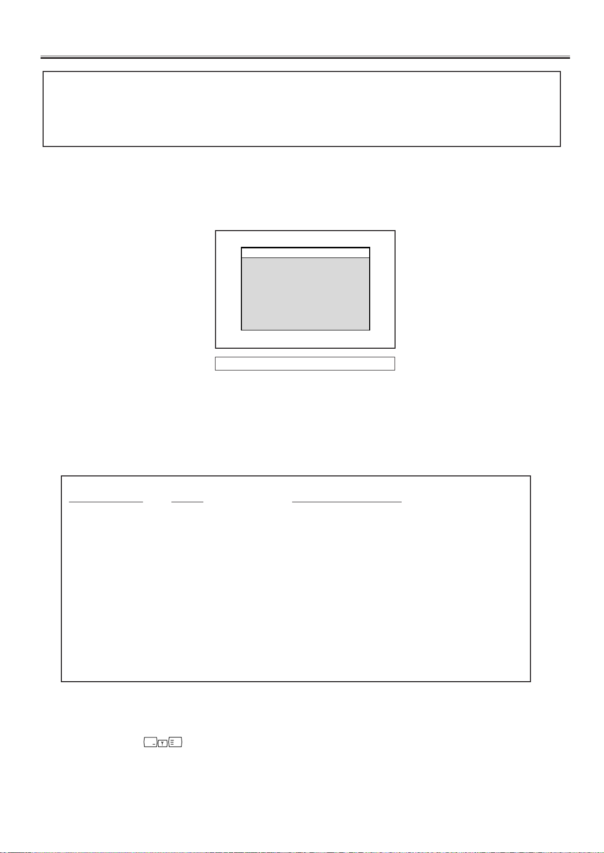
CUT-OFF ADJUSTMENT
1. Select AV mode with no signal input.
2. Enter the service mode (see pages 5&6) and select
mode “Regular”, item “02”. A horizontal line will appear
on the screen.
3. Adjust the Screen VR on the FBT to obtain the one
colour to be just visible.
4. By using the buttons 1, 2, 4, 5, 7, 8 on the remote
control, adjust the line to be white.
The key allocation is as follows;
Button No. Operation
1 Increase Red
2 Decrease Red
4 Increase Green
5 Decrease Green
7 Increase Blue
8 Decrease Blue
DRIVE ADJUSTMENT
5. Receive the white raster signal.
6. Select item “03 GRY”.
7. Adjust [R-Drive] and [B-Drive] control to obtain proper
white balance by using LEVEL+ or LEVEL - button.
a) Select [R-Drive] or [B-Drive] by using the P▲or
P▼button.
b) Adjust [R-Drive] or [B-Drive] by using the LEVEL+
or LEVEL - button.
8. Exit the service mode (see page 7).
1. Receive circular pattern .
2. Enter the service mode (see pages 5&6) and select
mode “Image”, item “02 P H-P”.
3. Press the LEVEL+ or LEVEL - button to adjust
horizontal centre.
4. Exit the service mode (see page 7).
1. Receive circular pattern.
2. Connect a digital volt-meter to both terminals of R453,
and a high voltage meter to CRT anode.
3. Confirm high voltage to be 25.0KV ± 1 KV at beam
current reading 1.1mV (21”).
HIGH-VOLTAGE CONFIRMATION
HORIZONTAL POSITION ADJUSTMENT