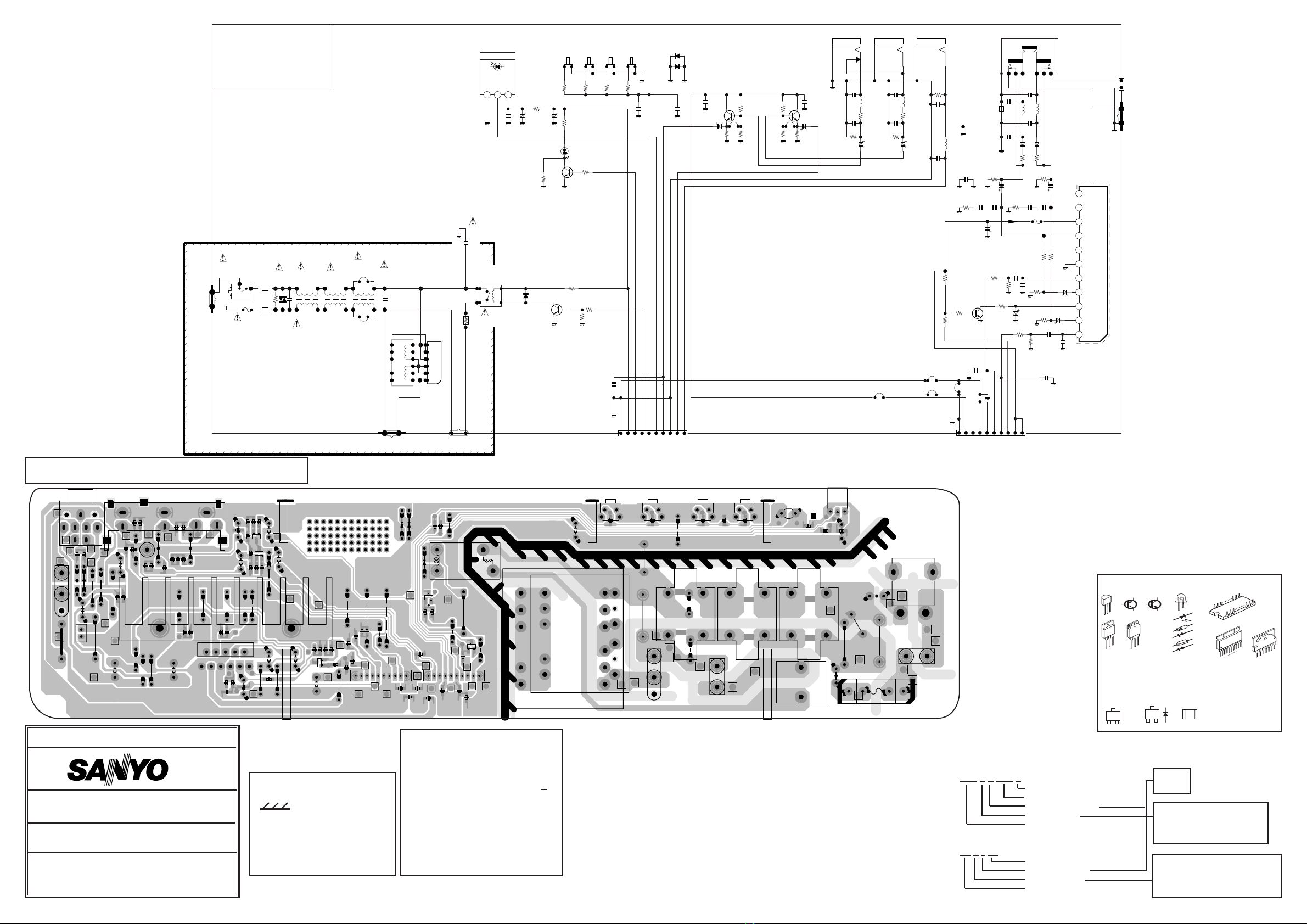
Part No. SKP20404 C6ALL (SHEET 1-5)
COLOUR TELEVISION
WW
WWBB
BB66
66--
--AA
AA
SERVICE REF.NO.
MODEL NUMBER
CHASSIS SERIES
CE28FWH2F-C-00
CE28FWH2F-C
The service Precaution:
The area enclosed by this line
( ) is directly connected
with AC mains voltage. When
servicing the area, connect an
isolating transformer between
TV receiver and AC line to elim-
inate hazard of electric shock.
Product safety notice:
Product safety should be considered
when a component replacement is
made in any area of a receiver.
Components indicated by a mark /!\ in
this circuit diagram show components
whose values have special significance
to product safety. It is particularly rec-
ommended that only parts specified on
the part service manual be used for
components replacement pointed out
by the mark.
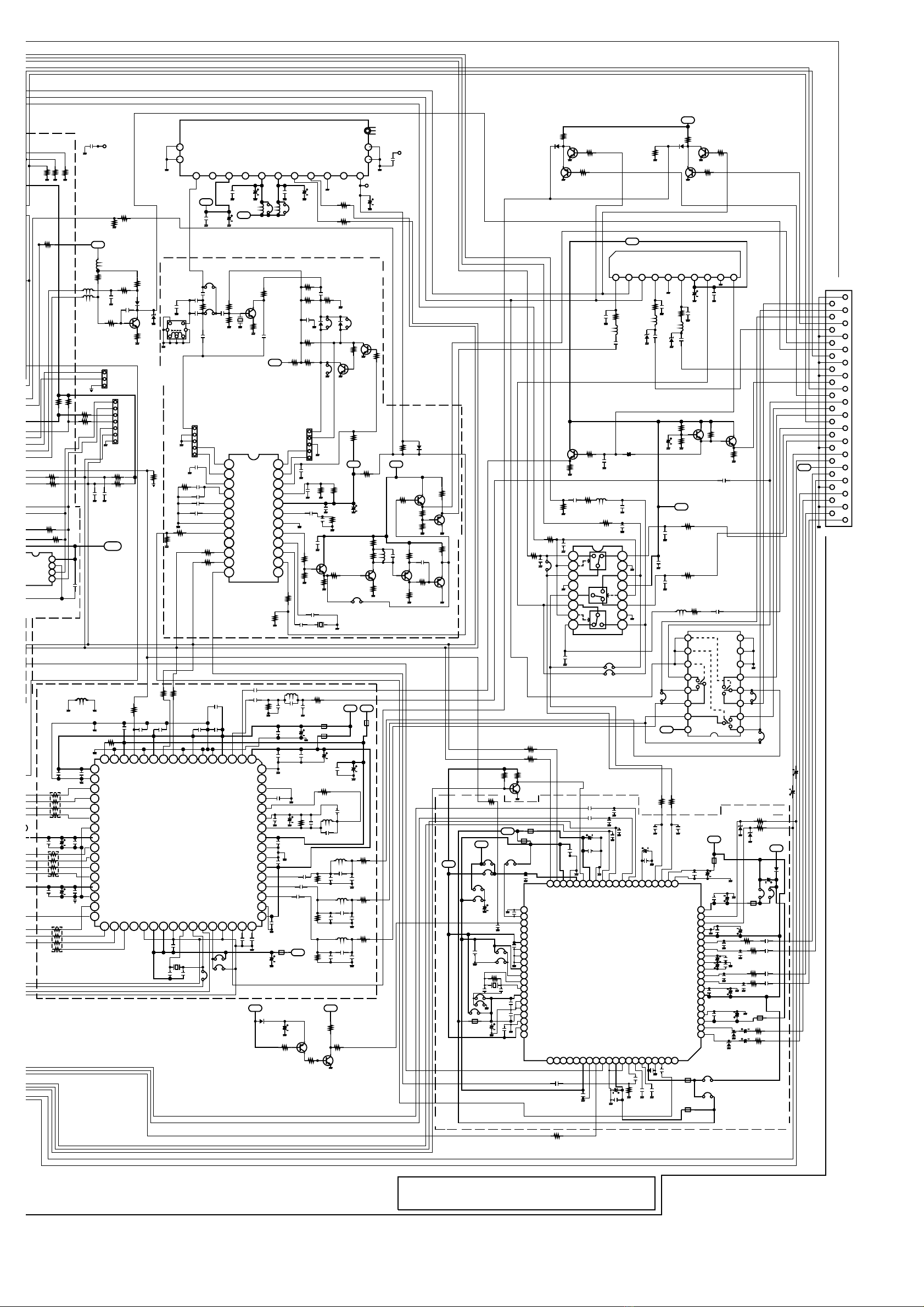
Circuit diagram notes :
1. All resistance values are in ohms, K=1,000, M=1,000,000.
2. All resistance rated wattages are 1/6W unless otherwise noted.
3. Excepting electrolytic capacitors, all capacitance values of less
than 1 are expressed in µF and more than 1 are pF.
4. All capacitance rated voltages are 50V unless otherwise noted.
5. All inductance values are in µH.
6. Voltage readings taken a digital voltmeter are from point indi-
cated chassis ground. Voltage readings taken by using a colour
bar signal are with all controls at normal position. Some volt-
ages may vary with signal strength.
7. Waveforms were taken with colour bar and controls adjusted
for normal picture. Waveforms were taken by using a wide
band oscilloscope and a low capacity probe.
8. This circuit diagram covers a basic or
representative chassis only. There
may be some components or partial
circuit differences between the actual
chassis and the circuit diagram.
9.■Diode 1S1555 may be replaced with
1S2473,1S2076 or DS472 unless
otherwise noted.
■ Transistor 2SC536(Q,R,S),
2SC1740(Q,R,S), 2SC945A(Q,R,P)
or 2SC1815(G,O,Y) unless other-
wise noted.
■Transistor 2SA608(E,F) may be
replaced with 2SA933(Q,R),
2SA564(QA,RA), or 2SA1015(O,Y)
unless otherwise noted.
Expression of capacitance and resistance in circuit diagram.
Capacitance (Example)
1000 C M 2000 D Characteristic
Capacitance value (220pF)
Tolerance (±20%)
Kind(Ceramic)
Rated voltage (1,000V)
Resistance (Example)
1/2 N J 1.2 Resistance value (1.2Ω)
Tolerance (±5%)
Kind (M.carbon)
Rated wattage(1/2W)
D : Carbon
N : Metallized carbon
S : Oxide metallized
W : Wire wounding
C : Solid
T, A, U, D : Electrolytic
C, K, B : Ceramic
F : Mylar film
M, N : Polypropylene
Z : Metallized paper
J= ± 5%
K= ± 10%
M= ± 20%