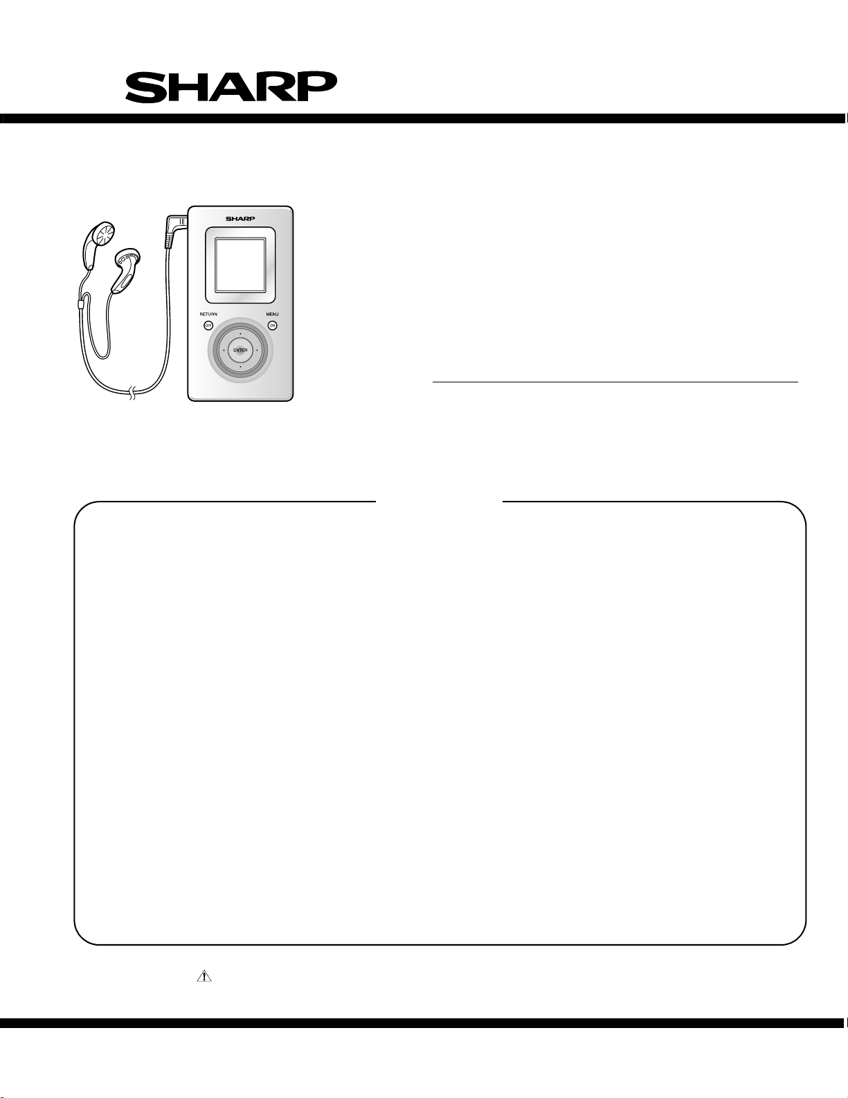
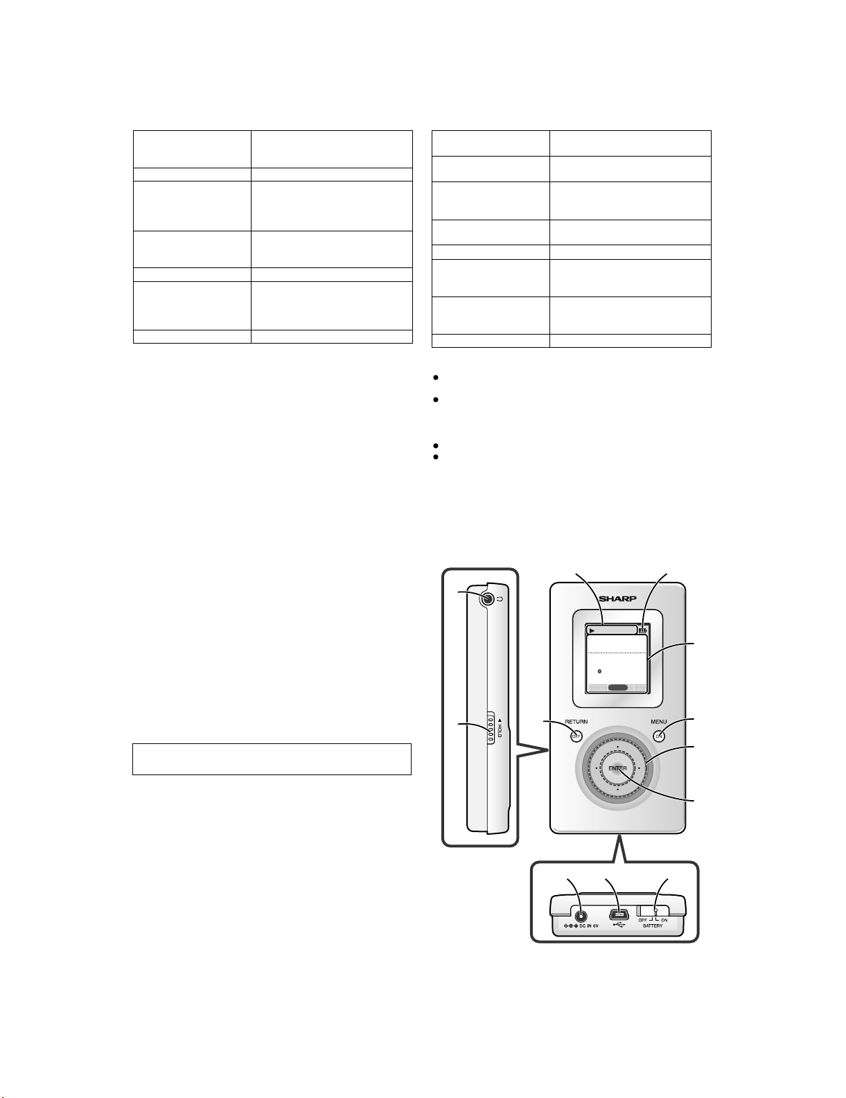
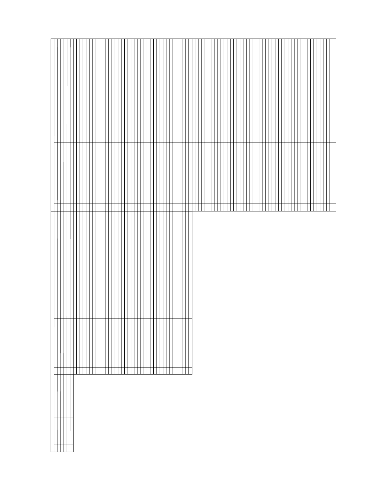
Sharp HR-MB3 User manual

HR-MB3
SERVICE MANUAL
No. XXXXXXXXXXXXX
SHARP CORPORATION
CONTENTS
Parts marked with " " are important for maintaining the safety of the set. Be sure to replace these parts with specified ones for
maintaining the safety and performance of the set.
This document has been published to be used
for after sales service only.
The contents are subject to change without notice.
CHAPTER 1. GENERAL DESCRIPTION
[1] Specifications ................................................. 1-1
[2] Names of parts............................................... 1-1
CHAPTER 2. ADJUSTMENTS
[1] TEST Mode .................................................... 2-1
[2] Error History Display ...................................... 2-2
[3] Error Code List ............................................... 2-3
[4] Updating the firmware .................................... 2-4
[5] Replacing the HDD unit.................................. 2-4
[6] Downloading the latest firmware .................... 2-4
CHAPTER 3. MECHANISM BLOCKS
[1] Caution on diassembly................................... 3-1
CHAPTER 4. DIAGRAMS
[1] Block diagram ................................................ 4-1
CHAPTER 5. CIRCUIT DESCRIPTION
[1] Notes on schematic diagram.......................... 5-1
[2] Types of transistor.......................................... 5-1
[3] Waveforms of circuit....................................... 5-2
[4] Voltage ........................................................... 5-3
CHAPTER 6. CIRCUIT SCHEMATICS AND PARTS
LAYOUT
[1] Schematic diagram........................................6-1
[2] Wiring side of PWB......................................6-13
CHAPTER 7. FLOWCHART
[1] Troubleshooting .............................................7-1
CHAPTER 8. OTHER
[1] Function table of IC .......................................8-1
Parts Guide
PORTABLE JUKEBOX
MODEL HR-MB3(S)

HR-MB3
– i –
1. Employing lead-free solder
"Main PWB" of this model employs lead-free solder. The LF symbol indicates
lead-free solder, and is attached on the PWB and service manuals. The alphabetical character following LF shows the type of
Example:
Indicates lead-free solder of tin, silver and copper.
2. Using lead-free wire solder
When fixing the PWB soldered with the lead-free solder, apply lead-free wire solder. Repairing with conventional lead wire solder
may cause damage or accident due to cracks.
As the melting point of lead-free solder (Sn-Ag-Cu) is higher than the lead wire solder by 40 C, we recommend you to use a
dedicated soldering bit, if you are not familiar with how to obtain lead-free wire solder or soldering bit, contact our service station
or service branch in your area.
3. Soldering
As the melting point of lead-free solder (Sn-Ag-Cu) is about 220 C which is higher than the conventional lead solder by 40 C,
and as it has poor solder wettability, you may be apt to keep the soldering bit in contact with the PWB for extended period of
time. However, Since the land may be peeled off or the maximum heat-resistance temperature of parts may be exceeded,
remove the bit from the PWB as soon as you confirm the steady soldering condition.
Lead-free solder contains more tin, and the end of the soldering bit may be easily corrected. Make sure to turn on and off the
power of the bit as required.
If a different type of solder stays on the tip of the soldering bit, it is alloyed with lead-free solder. Clean the bit after every use
of it.
When the tip of the soldering bit is blackened during use, file it with steel wool or fine sandpaper.
Be careful when replacing parts with polarity indication on the PWB silk.
Lead-free wire solder for servicing
Ref No. DescriptionParts No.
PWB-A 92LPWB6362HDDS Main
lead-free solder.
CAUTION
Danger of explosion if battery is incorrectly replaced.
Replace only with the same or equivalent type.

HR-MB3
1 – 1
AudioHR-MB3Service ManualHR-MB3MarketE
CHAPTER 1. GENERAL DESCRIPTION
[1] Specifications
[2] Names of parts
Power source: DC 6 V: AC adaptor
(AC 100 - 240 V, 50/60 Hz)
DC 5 V: USB bus power
Power consumption: 7 W (switching type AC adaptor)
Charging time: Approx. 4 hours
(fully charged, when using the
AC adaptor included with the
unit)
Dimensions: Width: 56.5 mm (2-1/4")
Height: 17.4 mm (11/16")
Depth: 105.5 mm (4-5/32")
Weight: 113 g (0.25 lbs.)
Sockets: Earphones
(impedance: 32 ohms)
USB (Exclusive type)
DC input
Frequency response: 20 - 20,000 Hz
Audio format: WMA (CBR/VBR),
MP3 (CBR/VBR), WAV (PCM)
Bit rate: WMA (32 - 320 kbps),
MP3 (8 - 320 kbps)
Sampling frequency: WMA(8-48kHz),
MP3(8-48kHz),
WAV (22.05 - 48 kHz)
Music MetaData: ID3 Tag (Version 1.0/1.1/2.3/
2.4), WMA object
Storage media: 4 GB hard disk drive (1 inch)
Output level: Earphones: 5 mW + 5 mW
(maximum output level/32
ohms)
Battery life: Up to 20 hours of continuous
playback by fully charged re-
chargeable Lithium-ion battery
PC interface: USB 1.1/2.0
Notes:
A combination of sampling frequency and bit rate dif-
fers depending on audio format.
Continuous playback:
At 128 kbps, in MP3 format (earphone output: 0.1 mW
+ 0.1 mW, backlight: not set to "Always", equalizer: set
to "Flat")
Actual battery life will vary with use.
The values are the standard values when the unit is
used at an ambient temperature of 25°C (77°F).
1. Earphones Socket
2. Hold Switch
3. Play Mode/Information Indicator
4. Battery Indicator
5. Return/Power Off Button
6. Character/Time/
Information Indicator
7. Menu/Power On Button
8. Cursor Button
9. Play/Stop/Enter/Power On Button
10.6VDCInputSocket
11. USB Socket (Exclusive type)
12. Battery Switch
Normal
1:00[3/8]
STOP
Music Name1
Artist Name1
Album Name1
1
3
5
9
6
7
8
2
10 11 12
4
The display varies depending on the operation.
The display language can be changed (default: En-
glish).

HR-MB3
2 – 1
AudioHR-MB3Service ManualHR-MB3MarketE
CHAPTER 2. ADJUSTMENTS
[1] TEST Mode
Entering/exiting test mode
Screen
Songs ***
Total Space ***
Free Space ***
Version *.***
TEST MODE
Version *.***
EEPROM **
No
Yes
EXIT TEST MODE
Exit
Change & Exit
Default load
Yes
No
Yes
No
No
Yes
Yes
No
No
Yes
About
Open "About" screen from MENU.
Enter test mode standby and display the version of
the firmware and Parameter.
To enter test mode, press these keys in the following
order:
MENU key
RIGHT key
DOWN key
UP key
RIGHT key (Press for 2 seconds.)
RETURN key ?
Test mode ends, and the TOP screen
appears.
Check that Parameter is updated and EXIT is
displayed.
Use UP key and DOWN key to select EXIT,
Change & Exit or Default load.
Update the specified area of Parameter.
MENU key ?
RETURN key ?
EXIT selected ?
Change & Exit selected ?
Write the default data for Parameter on
to Parameter.
ENTER key ?
1
2
3
4
5

HR-MB3
2 – 2
[2] Error History Display
Error history display
Screen
E-DATA
No
Yes
E-DATA
********
Yes
No
Yes
*********: Error code
No
No
Yes
E-DATA
Yes Clear?
No
Yes
No
No
Yes
Error history appears.
Error history content appears.
Use UP key and DOWN key to scroll.
*The latest history to be displayed in most significant
*Up to 10 error history records are displayed.
History clear mode.
ENTER key ?
ENTER key ?
ENTER key ?
RETURN key ?
MENU key ?
History is cleared.
Test mode switches to standby.
Test mode standby.
RETURN key ?
MENU key ?

HR-MB3
2 – 3
[3] Error Code List
Error Code List
How to read
TYPE VIEW CODE
num Type error num Type error num Type error
01 ETYPE_DS_ERROR Error from Data Server. 01 EVIEW_LOW_BATTERY_PLAY Battery has become low during playback. 0001 REALTIME_FAIL
02 ETYPE_UI_ERROR Error in UI. 02 EVIEW_NOT_OPEN_MASTERTBL Cannot open MASTER.TBL. 0002 DECODE_ERROR
04
ETYPE_BATT_ERROR
Battery error. 03 EVIEW_READERR_MASTERTBL Read error when reading MASTER.TBL 0003 REC_MEDIA_FULL
08 ETYPE_DB_ERROR Error from DB. 04 EVIEW_INVALID_MASTERTBL MASTER.TBL is invalid or the file format is not supported. 0004 MEDIA_NOT_READABLE
10
ETYPE_MKPL_ERROR
Error when creating default playlist.
05 EVIEW_CANT_FIND_FILE_DIR Cannot search files or folders. 0005 MEDIA_NOT_AVAILABLE
06 EVIEW_FILE_NOT_OPEN Cannot open MP3, WMA or WAV file. 0006 MEDIA_NOT_WRITABLE
07 EVIEW_READ_ERR_TAG Read error when searching for tag of MP3, WMA or WAV file. 0007 BAD_MEDIA
08 EVIEW_INVALID_TAG Tag of MP3, WMA or WAV file is invalid or not supported. 8001 MSG_FILE_NOT_FOUND
09 EVIEW_CANT_DEL_MASTERTBL Cannot rename/delete the existing MASTER.TBL. 8002 MSG_EMPTY_FILE
0A
EVIEW_CANT_CREATE_MASTERTBL
Cannot create a new MASTER.TBL. 8003 MSG_META_DATA_NOT_FOUND
0B EVIEW_WRITE_ERR_MASTERTBL MASTER.TBL write error. 8005 MSG_INVALID_META_TYPE
0C EVIEW_NOT_FREE_MASTERTBL Free space is likely to become insufficient when writing MASTER.TBL. 8007 MSG_UNSUPPORTED_BITRATE
0D EVIEW_USER_STOP_MASTERTBL Writing MASTER.TBL has been interrupted at the user's request. 8008 MSG_UNSUPPORTED_SAMPLERATE
0E
EVIEW_LOW_BATTERY_MASTERTBL
Writing MASTER.TBL has been interrupted due to low battery. 8009 MSG_AIC23_WRITE_FAILURE
0F
EVIEW_UNKNOWN_STOP_MASTERTBL
Writing MASTER.TBL has been interrupted due to sudden power cut, etc. 800A MSG_INVALID_AIC23_REG_ADDR
10
EVIEW_FILE_NOT_FOUND_MASTERTBL
No target file was found when creating MASTER.TBL. 800B MSG_INVALID_MONO_MODE
11 EVIEW_FILE_NOT_FOUND_REC Cannot find the existing file list . 800D MSG_INVALID_VOL_LEVEL
12 EVIEW_CANT_CREATE_REC Cannot create a new WMA or WAV file. 8010 MSG_NO_CHANNELS_AVAILABLE
13 EVIEW_CANT_CREATE_DIR_REC Cannot create a directory. 8011 MSG_INVALID_CHANNEL_ID
14 EVIEW_WRITE_ERR_REC WMA or WAV file write error. 8012 MSG_FAILURE
15 EVIEW_MAX_FILE_SIZE_REC
File size limit (FAT32: 4G) has been or is likely to be exceeded when writing WMA or WAV file
8014 MSG_EOF
16 EVIEW_NOT_FREE_REC Free space has or is likely to become insufficient when writing WMA or WAV file. 8015 MSG_MEDIA_NOT_AVAILABLE
17 EVIEW_LOW_BATTERY_REC Writing WMA or WAV file has been interrupted due to low battery. 8016 MSG_MEDIA_FULL
18 EVIEW_UNKNOWN_STOP_REC Writing WMA or WAV file has been interrupted due to sudden power cut, etc. 8017 MSG_FILE_IN_USE
19 EVIEW_NOT_OPEN_PLAYLIST Cannot open the specified M3U or PLS file. 8019 MSG_DIRECTORY_NOT_EMPTY
1A EVIEW_PLAY_ERROR_PLAYLIST Read error during playback of M3U or PLS file. 801A MSG_DUPLICATE_FILENAME
1B
EVIEW_DIR_NOT_FOUND_PLAYLIST
Cannot find the existing file list. (Cannot find a directory.) 801B MSG_INVALID_FILE_TYPE
1C EVIEW_CANT_CREATE_PLAYLIST Cannot create a new M3U or PLS file. 801F MSG_BOF
1D EVIEW_READ_ERR_PLAYLIST M3U or PLS file read error. 8021 MSG_PARTIAL_LISTING
1E EVIEW_CANT_OPEN_PLAYLIST Cannot open the specified M3U or PLSfile. 8022 MSG_FIFO_EMPTY
1F EVIEW_WRITE_ERR_PLAYLIST M3U or PLS file write error. 8023 MSG_NOT_AVAILABLE
20 EVIEW_NOT_FREE_PLAYLIST Free space has become insufficient when writing M3U or PLS file. 8024 MSG_INVALID_FILE_FORMAT
21 EVIEW_USER_STOP_PLAYLIST Writing M3U or PLS file has been interrupted at the user's request. 8025 MSG_CHANNEL_IN_BROWSE
22 EVIEW_LOW_BATTERY_PLAYLIST Writing M3U or PLS file has been interrupted due to low battery. 8026 MSG_CHANNEL_NOT_IN_BROWSE
23
EVIEW_UNKNOWN_STOP_PLAYLIST
Writing M3U or PLS file has been interrupted due to sudden power cut, etc. 8028 MSG_MEDIA_TIMEOUT
24 EVIEW_LOW_BATTERY Low battery. 8029 MSG_BAD_MEDIA
25 EVIEW_BATTERY_ERR Battery error. 802A MSG_DIR_ID_NOT_A_DIRECTORY
26 EVIEW_FILE_ERROR File error. 802B MSG_INSUFFICIENT_BUFFER_SIZE
27 EVIEW_FILE_NONE No file exists. 802D MSG_UNEXPECTED_ERROR
28 EVIEW_DISK_ERROR Disk error. 802E MSG_UNSUPPORTED_FAT_TYPE
29 EVIEW_HOLD HOLD function is active. 802F MSG_UNSUPPORTED_FILE_FORMAT
2A EVIEW_INTERNAL_ERROR Internal error. 8030 MSG_UNSUPPORTED_BIT_AND_SMPL
8031 MSG_LSE_DRM_INIT_FAILED
8032
MSG_UNSUPPORTED_DIRECTORY_STRUCTURE
8033 MSG_UNSUPPORTED_MEDIA_SIZE
8034 MSG_DEFAULT_REC_FILE_LIMIT
8035 MSG_UNSUPPORTED_IMAGE_FORMAT
8036 MSG_UNSUPPORTED_IMAGE_SIZE
8037
MSG_UNSUPPORTED_NUMBER_OF_CHANNELS
8038 MSG_UID_NOT_IN_LIST
8039 MSG_FILE_ERROR
803A MSG_FILE_NOT_OPEN
803B MSG_INVALID_MODE
803C MSG_INVALID_TRACK_TYPE
803D MSG_CACHE_FULL
8200 DB_ERR
8201 DB_ERR_RECORD_LIMIT
8202 DB_FOLDER_DEPTH_LIMIT
8203 DB_DEFAULT_FOLDER_NOT_EXIST
8204 DB_ERR_FILE_CHECKSUM
8205 DB_ERR_CREATE_DIR
8206 DB_ERR_CREATE_FILE
8207 DB_ERR_NOT_MATCH_PROFILE
8208 DB_ERR_MEDIA
8209 DB_ERR_OPEN_FILE
820A DB_ERR_FILE_CORRUPT
820B DB_ERR_CLOSE_FILE
820C DB_ERR_READ_FILE
820D DB_ERR_WRITE_FILE
820E DB_ERR_OPEN_CHANNEL
820F DB_ERR_CLOSE_CHANNEL
8210 DB_ERR_CHDIR
8211 DB_ERR_DUPLICATE_FILENAME
8212 DB_INVALID_INDEX
8214 DB_ERR_CREATE_NEW_DB
8215 DB_ERR_RENAME_OLD_DB
8216 DB_ERR_NO_DB
8217 DB_ERR_NO_CHANNEL
8218 DB_ERR_CREATE_NEW_PLS
8219 DB_ERR_FILELIST
821A DB_ERR_DELETE_FILE
821B DB_ERR_SYSTEM
821C DB_ERR_PLS_ADD_SONG
821D DB_ERR_LOW_BATTERY
821E DB_ERR_NO_SONG
C001 eERR_BATT_CHARGE Charging error.
C002 eERR_BATT_POWER Power is low.
TYPE ** (2Byte) VIEW ** (2Byte) CODE **** (4Byte)
** ** ****
^^ ^^ ^^^^

HR-MB3
2 – 4
[4] Updating the firmware
1. Plug in the AC adaptor.
1. The charging mode is activated. Press the ENTER or MENU key to turn on the power.
2. Copy the firmware.
1. Connect to a PC with the USB cable.
2. Copy the UPGRADE.BIN to ROOT of the drive.
3. Disconnect the USB cable.
3. Execute update.
1. Press the RETURN key to turn off the power, and unplug the AC adaptor.
2. Plug in the AC adaptor again.
3. "UpdatingFW..." appears and the update starts.
4. After the update is completed, the charging mode is activated.
4. Perform the following:
1. From the Menu List, open the About screen and check the firmware version.
2. From the Menu List, execute Format.
3. From the Menu List, execute Default.
4. Enter the test mode, then from Exit test mode, execute Default load.
[5] Replacing the HDD unit
1. Replace the HDD unit.
2. Plug in the AC adaptor.
1. "HDD error" appears.
2. Press these keys in the following order:
• MENU KEY
• RIGHT KEY
• DOWN KEY
•UPKEY
• RIGHT KEY (Press for 2 seconds.)
3. "Formatting..." appears and the format starts.
4. Follow these onscreen instructions:
i) ConnectUSB
ii) CopyUpgrade.Bin
iii) UnplugUSB
3. Disconnect the USB cable. "UpdatingFW..." appears and the update starts.
After the update is completed, the charging mode is activated.
4. Perform the following:
1. From the Menu List, open the About screen and check the firmware version.
2. From the Menu List, execute Default.
3. Enter the test mode, then from Exit test mode, execute Default load.
[6] Downloading the latest firmware
1. Visit the following websites
1. "http://sharp-world.com/worldwide/index.html"....Except for U.K.
2. “http://www.sharp.co.uk/”...For U.K.

HR-MB3
3 – 1
AudioHR-MB3Service ManualHR-MB3MarketE
CHAPTER 3. MECHANISM BLOCKS
[1] Caution on diassembly
Caution on Disassembly
Follow the below-mentioned notes when disassembling the unit and reassembling it, to keep it safe and ensure excellent performance:
1. Take cassette tape, and compact disc out of the unit.
2. Be sure to remove the power supply plug from the wall outlet before starting to disassemble the unit.
3. Take off nylon bands or wire holders where they need to be removed when disassembling the unit. After servicing the unit, be sure to rearrange
the leads where they were before disassembling.
1 Bottom Cabinet 1. Screw ......................(A1) x5
2MainPWB
2. Socket ...................... (A2) x1
2. HDD Holder ..............(B2) x1
1. Screw ....................... (B1) x4
4. Solder Joints............ (B4) x2
6. Solder Joints.......... (B6) x35
7. LCD Unit .................. (B7) x1
3. Flexible PWB ........... (B3) x1
5. LCD Shield Case ..... (B5) x1
STEP REMOVAL PROCEDURE
Bottom Cabinet
Top Cabinet
(B2)x1
(A1)x3
M1.4x2mm (A1)x2
M1.4x5mm
Top Cabinet
Main PWB
HDD
(B1)x4
M1.4x4mm
(B5)x1
(B6)x33
(B4)x1
(B6)x2
(B4)x1
(B3)x1
(B7)x1
Main PWB
Pull
Pull
(A2)x1
Note: A special jig is necessary for the installation
of the LCD unit.

HR-MB3
4 – 1
AudioHR-MB3Service ManualHR-MB3MarketE
CHAPTER 4. DIAGRAMS
[1] Block diagram
J400
DC SOCKET
6V OUTPUT
SC200
USB SOCKET
5V OUTPUT
P401
Li-ion Battery
3.7V OUTPUT
S401
BATTERY SW
START UP
CIRCUIT
D401, Q403
Li-ion
CHARGE & POWER MANAG
4
20
15~17
5, 6
Q1
IC400
BQ24032
IC403
TPS62220
IC401
TPS62200
IC404
TPS62220
BACK LIGHT
KEY INPUT
IC302
1112B31M
3.1V
REGULATOR
IC405 MM3097
IC402 TPS72201
Q3 Q2
DC/DC DOWN
3.3V
(400mA Class)
DC/DC DOWN
1.6V
(300mA Class)
DC/DC DOWN
3.3V
(400mA Class)
DC/DC UP
7.5V
20mA
LCO MODULE
3.3V
1.6V REGULATOR
3.3V
3.3V
1.6V
29~39
42,44,45,47,48
50,51,53
3
3
3
4
1
16~28, 30
IC100
TMS320DA255
DSP
HDD UNIT
3.3V IC201
CY68013A
USB2.0(Slave)
IC202
BR24L64F
EEPROM
1.6V (CORE)
1.6V (RTC)
3.3V
J300
HEADPHONES
IC302
3.1V
9,10
5,6
23,24,25
3.3V
19,25,26,29,31,33
37~48
2,4,5,7,8
10,11,13,
15~26
8,9
5,6
15,16
AUDIO DAC
IC301
TLV320DAC23
IC503
AT24C512
EEPROM
3~7
IC500
256 MB SDRAM
3.3V
1,2,8,9,18~25,29~31,
33~38,40,42,44~52
3,5~8,10,12~17
SIGNAL & DATA& CONTROL LINE
POWER SUPPLY LINE
Figure 4-1 BLOCK DIAGRAM (1/1)

HR-MB3
5 – 1
AudioHR-MB3Service ManualHR-MB3MarketE
CHAPTER 5. CIRCUIT DESCRIPTION
[1] Notes on schematic diagram
•Resistor:
To differentiate the units of resistors, such symbol as K and M are
used: the symbol K means 1000 ohm and the symbol M means
1000 kohm and the resistor without any symbol is ohm-type resis-
tor. Besides, the one with “Fusible” is a fuse type.
• Capacitor:
To indicate the unit of capacitor, a symbol P is used: this symbol P
means pico-farad and the unit of the capacitor without such a sym-
bol is microfarad. As to electrolytic capacitor, the expression
“capacitance/withstand voltage” is used.
(CH), (TH), (RH), (UJ): Temperature compensation
(ML): Mylar type
(P.P.): Polypropylene type
• Schematic diagram and Wiring Side of P.W.Board for this model are
subject to change for improvement without prior notice.
[2] Types of transistor
REF. NO DESCRIPTION POSITION
SW300 HOLD ON—OFF
SW301 RETURN/POWER OFF ON—OFF
SW302 MENU/POWER ON ON—OFF
SW303 FUNCTION ON—OFF
SW304 SKIP DOWN/SCROLL LEFT/REVIEW ON—OFF
SW305 VOLUME UP/SCROLL UP ON—OFF
SW306 VOLUME DOWN/SCROLL DOWN ON—OFF
SW307 SKIP UP/SCROLLRIGHT/CUE ON—OFF
SW401 BATTERY/CUT ON—OFF
REF. NO DESCRIPTION POSITION
TOP VIEW
TOP VIEW TOP VIEW
1SS400
RB520530
RB521S30
VDZS33B
VDZS8R2B
FS1J3TP
RB106M3
RN1104
RN2104
MCH3405
KDS121 E
B
(G)
(3)
E
(S)
(1)
C
(D)
(2)
TOP
VIEW

HR-MB3
5 – 2
[3] Waveforms of circuit
TL304
LOUT TL700
LCD_BL_POW
IC301: 4PIN IC405 4PIN
DIN SH
(LCD_BL_ON)
IC301: 5PIN TL415
LRCIN VCC 3.3V
IC301: 3PIN IC404 3PIN
BCLK EN
(P-CON)
PLAYBACK When it is started.
the time of the AC adapter starting
START LCD DISPLAY BEGINNING
TL414
HDD 3.3V
IC403 3PIN
EN
(HDD_ON)
TL415
VCC 3.3V
IC404 3PIN
EN
(P-CON)
POWER ON HDD START
POWER ON
HDD START
TL414
HDD 3.3V
IC403 3PIN
EN
(HDD_ON)
TL415
VCC 3.3V
IC404 3PIN
EN
(P-CON)
At the time of the battery actuation
Enter or Menu key push time

HR-MB3
5 – 3
[4] Voltage
VHITLV320D+-1 VHITPS62200-1 VHICY68013A-1 RH-IXB074WJZZ
IC301 IC401 IC201 IC500
1 3.1 V 1 4.4 V 1 P 1 3.2 V
20V 20V 2P
P
P
2P
3 P 3 5.1 V 3 3.2 V 3 3.2 V
4P
P
4P 4 4
550.5V55
666
7P
VHIBQ24032+-1 73.2V 7 P
P
P
8 3.1 V IC400 8 P 8 P
9 1.55 V 1 3.35 V 9 P 9 3.2 V
10 1.55 V 2 - 10 0 V
0V
10 P
11 0 V
0
3 0 V 11 3.2 V 11 P
12 1.55 V 4 5.65 V 12 0 V 12 0 V
0V
13 1.55 V 5 3.45 V 13 P 13 P
14 3.1 V 6 3.45 V 14 0 V 14 3.2 V
15 0 V 7 5 V 15 3.2 V 15 P
16 1.55 V 8 5.2 V 16 3.2 V 16 P
17 - 9 4.4 V 17 3.2 V 17 P
18 - 10 0.25 V 18 P 18 P
19 - 11 0 V 19 P 19 P
20 - 12 1.5 V 20 P 20 P
21 0 V 13 3.5 V 21 P 21 0 V
22 0 V 14 2.5 V 22 P 22 P
23 3.3 V 15 4.4 V 23 P 23 P
24 3.3 V 16 4.4 V 24 P 24 P
25 P V 17 4.4 V 25 P 25 P
26 0 V 18 0 V 26 0 V 26 P
27 2.7 V 19 0 V 27 3.2 V 27 3.2 V
28 0 V 20 4.85 V 28 0 V 28 0
29 P 29 P
VHIMM3097++-1 VHITC7SZ32U-1 30 P 30 P
IC405 IC200,502,700 31 P 31 P
1P
0V
1 P 32 3.2 V 32 P
2 2 P 33 P 33 P
3 0.986 V 3 0 V 34 P 34 P
4 3.3 V 4 P 35 P 35 P
5 4.4 V 5 3.2 V 36 P 36 P
37 P 37 3.2 V
VHI80827CNN-1 VHIBR24L64F-1 38 P 38 P
IC406 IC202 39 3.2 V 39 P
1 3.1 V 1 3.2 V 40 P 40 0 V
2 3.3 V 2 0 V 41 0 V 41 0 V
3 - 3 0 V 42 3.2 V 42 P
40V
P
0V
4 0 V 43 3.2 V 43 3.2 V
5 P V 44 3.2 V 44 P
VHITPS72201-1 6PV 45P 45P
IC402 7 0 V 46 P 46 0 V
1 4.4 V 8 3.2 V 47
48
P47P
2 P 48 P
3 4.4 V VHIAT24C512-1 49 P 49 3.2 V
4 1.2 V IC503 50 P 50 P
5 1.6 V 1 0 V 51 P 51 P
252P520V
VHITPS62220-1 30V
0V
53 0 V 53 P
IC403,404 4 0 V 54 P 54 0 V
1 4.4 V 5 P 55 3.2 V
20V 6P 560V
3 4.95 V 7 0 V
0V
4 0.485 V 8 3.2 V * P is a pulse.
5VHI1112B31M-1
IC302
1 3.3 V
2
3 3.3 V
4-
5 3.1 V

HR-MB3
5 – 4
—MEMO —

HR-MB3
6 – 1
AudioHR-MB3Service ManualHR-MB3MarketE
CHAPTER 6. CIRCUIT SCHEMATICS AND PARTS LAYOUT
[1] Schematic diagram
Figure 6-1 SCHEMATIC DIAGRAM (1/12)
A
B
C
D
E
F
G
H
123456
TL130
zCE3
FB101
33
R100
HDD_ON
CE_CONT
TL124
TL112
D1
CHARGE_ON/OFF_DET
0.1u
C111
DSP_RST
TL104
TL131
FB103
0.01u
C104
0
R102
TL122
CHARGER_CE_CONT
TL120
FB102
LCD_CS
33
R108
0.01u
C105
TL105
TL125
zRE
D3
4.7u/6.3V
C101
AC_DET
TL103
8P
C109
0.01u
C107
D6
LCD_RST
TL113
CVCC_CTL
D4
TL107
DCDC_EN
100K
R109
FB104
D2
X100
TL111
0
R116
0
R101
0
R104
TL100
TL123
D0
RTCDVDD1.6V
0.1u
C110
IC100
IXA068AW
DSP
153
154
155
156
157
158
159
145
146
147
148
149
151
150
152
143
144
136
137
136
137
138
139
140
141
142
160
161
162
163
164
165
166
167
168
169
170
171
172
173
174
175
176
177
178
179
106107108109110111112113114115116117118119120121122123124125126127128129130131132133134135
12 3 4 5 6 7 8 9 10 11 12 13 14 15 16 17 18 19 20 21 22 23 24 25 26 27 28 29 30
TL102
A10
TL121
TL116
A1
VCC3.3V
4.7u/6.3V
C102
0
R107
0
R111
TL129
TL126
FB100
TL110
TL101
zWE
D5
10uH
L100
TL109
0.1u
C106
0.01u
C114
8P
(CH) (CH)
C108
VCC1.6V
BATT_DET 4.7u/6.3V
C103
D7
GND
0.01u
C115
LCD_BL_ON
12P
(CH)
C122
TL106
TL108
0
R127
TL117
TL118
TL119
TL115
TL127
TL128
TL140
TL141
TL142
TL143
TL144
TL145
TL146
TL147
0
R103
0
R105
0
R130
47K
R131
TL149
33
R133
33
R132
33
R134
33
R135
0.1u
C124
0
R137
4.7u/6.3V
C125
4.7u/6.3V
C126
4.7u/6.3V
C129
0.01u
C127
0.01u
C128
0.01u
C130
R140
68K
10K
C112
zOE
HDD_ON
A14
HDD_RST
LCD_RST
A18
zBE1
EMU0
A15
zINT1
TRST
A0
zOE
BCLK
A0
zCE3
HDD_DMACK
TDI
USB_RDY
A15
SD_BA1
zSDCAS
A18
USB_CTL1
zWE
TCK
zCE1
CHARGER_CE_CONT
TDO
TCK’
zCE0
LCD_BL_ON
zRE
A11
LCD_CS
A16
DCDC_EN
zBE0
HDD_CS0
USB_CS
USB_DET
A16
AUDIO_MCLK
CVCC_CTL
zINT3
zINT4
AC_DET
A17
A19
A20
A17
A19
A20
BATT_DET
READY
zCE1
zCE2
KEYIN
FUNCTION_SW
EMU1
TMS
POW_ON_SW
CE_CONT
WAKEUP
ADJ_DET
SDATA_IN
LRCOUT
LRCIN
SDATA_OUT
CHARGE_ON/OFF_DET
CVDD6(B8)
RCVDD(C12)
C8(J4) BEO-
VSS2(C2)
VSS9(N14)
DVDD16(E6)
TO_POWER
P6-8 11-B
P6-10 1-E
C4(H4) CE0-/GPIO9
CVDD7(G1)
S24(B10)
MMC2.DAT2/FSR2
MMC1.DAT2/FSR1
RVDD2(L1)
DN(USB)(D3)
GPIO1(E1)
S10(D7)
RTCINX2(B12)
DX0(E7)
DVDD14(A8)
USBVDD(D2)
VSS14(B9)
VSS24(C5)
GPIO0(F3) S13(E9)
MMC2.DAT1/DR2
S15(E8)
X1(F1)
S12(A7)
C0(G5) GPIO.IO8//RE-
DVDD15(A4)
C7(J3) CE3-/GPIO11
S22(C9)
GPIO4(A3)
RDVDD3(A14)
GPIO2(E2)
VSS26(A2)
N.C.(EC3)
AVSS2(B14)
C3(H1) RDY
VSS13(B11)
CVDD9(N8)
TIN/TOUT0(B4)
N.C.(E10)
S25(D10)
MMC2.DAT0/CLKX2
FSX0(B6)
MMC1.DAT0/CLKX1
MMC1.DAT1/DR1
C2(G4) WE-
VSS6(P2)
S21(A10)
GPIO7(D1)
DVDD1(E3)
VSS18(P1)
C11(K3) SDCAS-
MMC2.DAT3/FSX2
VSS11(D11)
FSR0(A5)
MMC2.CLK/DX2
GPIO3(B3)
DVDD8(J2)
A20(G3)
VSS5(N2)
DVDD10(K10)
DP(USB)(D4)
C9(K2) BE1-
S23(A11)
VSS15(K4)
S20(A9)
GPIO6(C4)
CVDD4(C10)
CVDD13(A6)
DR0(D6)
DVDD7(H2)
C5(H5) CE1-/GPIO10
CLKOUT(F5)
AIN1(D13)
CLKR0(B5)
C6(J1) CE2-
VSS3(E4)
A18(K1)
S11(D8)
RDVDD2(A13)
C1(G2) OE-
S14(C8)
CVDD12(B7)
AVDD(C14)
VSS12(C11)
RTCINX1(A12)
X2/CLKIN(F2)
MMC1.CLK/DX1
A14(K9)
GPIO5(D5)
AIN2(D12)
CLKX0(C6)
12MHz
A16(P7)
MMC1.DAT3/FSX1
AVSS1(C13)
A’[0](H11)
CVDD8(J5)
CVDD1(B2)
VSS25(E5)
RDVDD1(B13)
TO_LCD
DVDD3(N13)
A19(H3)
VSS4(F4)
PU(USB)(C1)
A15(M8)
MMC2.CMD/CLKR2
DVDD6(D9)
VSS23(C7)
A17(P5)
DVDD12(P14)
DVDD11(P13)
AIN3(E11)
VSS1(B1)
MMC1.CMD/CLKR1
• NOTES ON SCHEMATIC DIAGRAM can be found on page 5-1.
MAIN PWB-A (1/6)
+B +B
+B
+B +B +B
+B
+B
+B
+B
+B
+B +B +B
+B
+B
+B
+B
+B +B +B

HR-MB3
6 – 2
Figure 6-2 SCHEMATIC DIAGRAM (2/12)
78 9 10 11 12
D9
A14
zCE3
TL133
D10
TL138
zBE0
DSP_RST
A13
D13
zINT2
SDA
D2
A7
SDA
A2
D6
A3
zRE
0.1u
C120
A1
D4
USB_CS
100K
R114
D6
D8
USB_RDY
0.01u
C116
D8
0.01u
C117
TL131
D9
1.5K
R122
D11
KEYIN
TL132
A10
TL135
D13
1
20
D7
zWE
HDD_DMACK
D5
D3
A14
zCE3
TL139
D12
D11
A8
A2
100K
R125
D10
zCE0
POW_ON_SW
zINT0
zBE1
zSDCAS
SCL
D15
TL134
A4
USB_CTL1
AUDIO_MCLK
zWE
D5
0
R126
100K
R120
0.01u
C119
TL136
USB_DET
LRCOU T
A9
zRE
TL137
HDD_CS1
0.1u
C118
D0
SCL
FUNCTION_SW
SD_BA 1
D14
TL114
SDATA_OUT
47
48
46
47
46
50
51
49
53
54
52
56
57
55
58
60
61
59
62
64
65
63
66
68
69
67
70
72
73
71
74
75
77
78
76
79
80
82
83
81
84
85
86
88
89
90
89
90
919293949596979899100101102103104105106107108109
0
87
6
27 28 29 30 31 32 33 34 35 36 37 38 39 40 41 42 43 44 45
READY
zSDWE
A6
D1
D3
zSDRAS
D12
D15
A5
TL121
D7
HDD_RST
LRCIN
XF
CLKMEM
A3
D1
D4
HDD_CS0
BCLK
1.5K
R123
0
R115
SDA10
D0
100K
R118
A12
D2
0
1u
1
14
0.01u
C121
A1
D14
SDATA_IN
100K
R124
100K
R117
0.01u
C115
100K
R129
*VA103
WAKEUP
ADJ_DET
ADJ_DET
33
R136
0.01u
C131
0.01u
C133
0.01u
C132
A11
D14
D0
A3
A8
A6
zBE1
TDI
zSDWE
TCK’
D6
SCL
D15
A10
D9
D5
A1
zSDCAS
A4
D3
D7
A7
D1
D13
D8
XF
TDO
A5
A2
A9
D4
TMS
D2
TRST
zINT4
zINT2
zINT0
zINT3
zINT1
BATT_DET
D12
SDA
D11
D10
TCK
zSDRAS
SDA10
A12
A13
KEYIN
DSP_RST
CLKMEM
C(C)
()
INT1_(G13)
XF(E14)
CVDD2(M4)
INT0_(G14)
RVDD2(L1)
EMU0(K11)
RVDD1(J10)
A6(L6)
EMU1/OFF(K12)
A10(N4)
TDO(K13)
AIN0(D14)
TCK(J13)
TMS(J14)
C10(M1) SDRAS-/GPIO12
INT3_(F14)
D1(K8)
DVDD4(M12)
A0/A14(L7)
D11(N12)
TDI(K14)
TRST_(J12)
VSS17(N1)
INT2_(G10)
D3(M9)
D4(L9)
CVDD11(G11)
ADVSS(E12)
A3(K6)
D13(L11)
CVDD5(J11)
D2(P9)
VSS16(K5)
D10(P12)
A13(N3)
D9(L10)
D5(P10)
D15(L13)
D12(M14)
C12(L3) SDWE- ADVDD(F10)
VSS19(N9)
C11(K3) SDCAS-
TO_AIO
VSS10(M13)
A12(P3)
CVDD3(L14)
DVSS(G12)
DVDD9(P8)
A2(K7)
TO_USB
VSS8(M5)
A11(L4)
D7(P11)
DVDD5(H10)
CVDD10(M11)
C9(K2) BE1-
C14(L2) CLKMEM
VSS22(E13)
D0(L8)
VSS21(F11)
AIN1(D13)
A4(P6)
SCL(H14)
DVDD13(F13)
VSS7(M3)
INT4_(F12)
A1(M7)
A9(P4)
TO_MEMORY
AVDD(C14)
DVDD2(N6)
D6(M10)
SDA(H13)
A8(L5)
C13(M2) SDA10/GPIO13
RVDD3(N7)
AVSS1(C13)
VSS20(N10)
CVDD8(J5)
RDVDD1(B13)
RESET_(H12)
A7(N5)
D14(L12)
A5(M6)
D8(N11)
P6-9 1-D
P6-5 1-E P6-3 1-D
+B
+B
+B
+B
+B
+B
+B
+B
+B
+B +B
+B
+B

HR-MB3
6 – 3
Figure 6-3 SCHEMATIC DIAGRAM (3/12)
P6-8 11-G
P6-2 12-E
0.1u
C200
D15
150K
R200
D0
A14
D2
D1
A1
TL206
D9
D11
zWE
zINT0
0
R210
A2
IC200
TC7SZ32U
2 INPUT OR GATE
12 3
45
D8
zRE
0.1u
C201
12P(CH)
C203
FB200
USB_CS
GND
D14
100K
R209
IC201
CY68013A
USB 2.0
123456789
343536373839404142
43
44
45
46
47
48
49
50
51
52
53
54
55
56
USB_CTL1
USB_DET
0.01u
C204
D6
FB201
USB_VBUS
D4
USB_RDY
VCC3.3V
X200
D7
2.2K
R207
D12
120K
R201
TL200
12P
(CH)
C202
A3
D3
D10
D5
zCE3
DSP_RST
D13
WAKEUP
ADJ_DET
0.1u
C208
0.1u
C209
4.7u
C206
4.7u
C207
0
R217
zINT0
USB_VBUS
A1
D10
A3
USB_CS
D9
D11
zCE3
D12
A2
D14
DSP_RST
D15
/SLCS
zRE
/SLCS
D8
USB_DET
USB_DP
D13
zRE
USB_DN
zWE
WAKEUP
VCC
RESET
CLKOUT
PD7
GND
PD1
WAKEUP
GND
AGND
TO_ASIC
WU2
XTALI N
AVCC /SLCS
TO POWER
VCC
PD4
PA1
AVCC
FIFOADR0
PD0
PKTEND
SLOE
DMINUS
SLRD
PD2
SLWR
PD3
PD5
GND
GND
DPLUS
XTALOUT
VCC
FIFOADR1
PD6
24MHz
A
B
C
D
E
F
G
H
123456
• NOTES ON SCHEMATIC DIAGRAM can be found on page 5-1.
MAIN PWB-A (2/6)
+B
+B
+B
+B +B
+B
+B
+B +B
+B +B

HR-MB3
6 – 4
Figure 6-4 SCHEMATIC DIAGRAM (4/12)
SC200
USB TERMINAL
1
2
3
4
5
TL205
TL204
FB202
47K
R204
TL202
0.01u
C205
BR24L64F
IC202
IC202
TZA004AW
EEPROM
1234
5678
FB203
100K
R203
C
201
6
8013A
S
B 2.0
89
10 11 12 13 14
15
16
17
18
19
20
21
22
23
24
25
26
27
28
29303132333435
TL208
TL203
10K
R205
TL210
TL201
100K
R206
TL207
TL209
3.3K
R215
3.3K
R214
L201
0
R212
0
R213
0
R216
0.1u
C210
0.1u
C211
USB_DP
zINT0
D2
D4
D5
D1
D6
zRE
D3
D7
USB_DP
D0
USB_RDY
USB_DN
USB_VBUS
USB_DN
USB_CTL1
GND
CTL0
SDA
PB7
SCL
RESERVED
A1
VCC
CTL1
VCC
PB0
GND
VBUS
A0 GND
PA0
GND
T0OUT
PA1
+D
-D
PB2
CTL2
PB6
USB_CONN 2.0
PB4
SLOE
DMINUS
SCL
ID(NC)
VCC
PB5
GND
A2
PB1
SDA
VCC
DPLUS
AGND
VCC
WP
PB3
78 9 10 11 12
+B
+B
+B
+B
+B
+B
+B

HR-MB3
6 – 5
Figure 6-5 SCHEMATIC DIAGRAM (5/12)
0
R319
0
R322
0
R324
SDA
SCL 100
R308
100u/4
V
C31
0
GND
0.1u
C309
10u/6.3V
C301
0
R317
0
R318
SDATA_OUT
AUDIO_MCLK
100
R309
0
R
3
100
R310
100
R312
100K
R316
100K
R314
LRCOUT
SDATA_IN
0
R313
100
R315
33
R311
TL300
33
R306
TL302
10u/6.3V
C300
BCLK
0.1u
C303
0
R304
TL301
VCC3.3V
LRCIN
0.1u
C302
FUNCTION_SW
POW_ON_SW
KEYIN
0.1u
C306
10u/6.3V
C307 10u/6.3V
C308
100K
R331
100K
R332
22K
R333
FUNCTION_SW2
POW_ON_SW2
TL311
TL309
TL
3
RB520S30
D301 RB520S30
D302
1
2
3
4
SW302
MENU/
POWER ON
SW303
FUNCTION
SW300
HOLD
1
2
3
41
2
3
RB521S30
D303
RB521S30
D304
IC301
12345678910 11 12 13 14
1516171819202122232425262728
0
R301
IC302
1112B31M
3.1V
REGULATOR
VCC
1
GND
2
EN
3
N.C.
4
VOUT
5
1u
C316
1u
C317
0.01u
C318
0.01u
C319
0.01u
C320
0.01u
C321
0
R342
LRCOUT
LRCIN
SDATA_OUT
BCLK
SDATA_IN
AUDIO_MCLK
FUNCTION_SW
POW_ON_SW
SDA
SCL
POW_ON_SW2
FUNCTION_SW2
(2.7--3.6V)
XTI/MCLK
HPVDD
RHPOUT
LRCIN
DVDD
(2.7--3.6V)
DIN
MICBIAS
VMID
CS-
MICIN
(1.42--3.6V)
BCLK
DGND
MODE
AGND
BVDD
SCLK
(2.7--3.6V)
LRCOUT
RLINEIN
LLINEINLHPOUT
ROUT
TO_ASIC
HPGND
DOUT
XTO
LOUT
TO_POWER
SDIN
AVDD
CLKOUT
A
B
C
D
E
F
G
H
123456
• NOTES ON SCHEMATIC DIAGRAM can be found on page 5-1.
P6-8 11-DP6-2 12-G
+B
+B
+B
+B
+B
+B
+B
+B
+B
+B
+B +B

HR-MB3
6 – 6
Figure 6-6 SCHEMATIC DIAGRAM (6/12)
0
R319 10K
R328
10K
R326
12K
R325
1.5K
R320
100u/4V
C310
TL305
TL303
0.1u
C309
0
R317
0
R318
0
R305
0.1u
C311
100u/6.3V
C312
TL304
TL302
100u/6.3V
C313
301
1K
R323
1K
R321
1
0u/6.3V
C308
VA301
130P
VA302
130P
27K
R329
22K
R333
TL310
TL314
TL313
TL312 TL308
TL307
TL306
27
R337
27
R338
J300
HEADPHONES
1
2
3
4
1
2
3
4
1
2
3
4
1
2
3
4
1
2
3
4
SW300
HOLD
SW304
SKIP DOWN/
SCROLL LEFT/
REVIEW
SW305
VOLUME UP/
SCROLL UP
SW306
VOLUME DOWN/
SCROLL DOWN
SW307
SKIP UP/
SCROLL RIGHT/
CUE
SW301
RETERN/
POWER OFF
1
2
3
12K
R330
IC301
TLV320D
AUDIO DAC
1
213 14
1516
1
7
0.0033
C314
0.0033
C315
0.01u
C318
0.01u
C319
0.01u
C320
0.01u
C321
68K
R344
68K
R345
0
R327
FB300
FB301
R_HPOUT
KEYIN
L_HPOUT
R_HPOUT
L_HPOUT
AUDIO_GND
MICBIAS
VMID
AUDIO-L_IN/OUT
AUDIO-R_IN/OUT
AGND
(2.7--3.6V)
ROUT
LOUT
AVDD
78 9 10 11 12
MAIN PWB-A (3/6)
+B

HR-MB3
6 – 7
Figure 6-7 SCHEMATIC DIAGRAM (7/12)
L400
1.6A/36V
F400 RB160M30
D400
T
10u/6.3V
C405
T
P
1
2
3
1
2
3
1
2
3
10u/6.3V
C406
10u/6.3V
C403
TPS
6
IC
1
2
3
10u/6.3V
C422
1u
C400 15K
R408
15K
R407
33K
R405
47K
R402
10u/6.3V
C402
TL400
TL401 TL403
10u/6.3V
C404
IC402
TPS72201
1.6V
REGULAT
O
KDS121E
D401
1
2
3
1K
R400
1K
R401
100K
R409
0.1u
C401
100K
R404
270K
R424
330K
R425
0.1u
C424
0
R428
0.1u
C425
1SS400
D404
1K
R437
TL404
TL405
TL407
TL406
TL408
TL409
TL410 TL411
10u
C427
10u
C429
1u
C430
MCH3405
Q404
S
D
G
3.3K
R436
10K
R430
10K
R429
560K
R433
RB520S30
D402
RB520S30
D405
KDS121E
D403
1
2
3
TL402
150K
R406
150K
R427
0.1u
C428
RN2104
Q403
P401
1
2
SW401
BATTERY ON/OFF
123
J400
DC IN 6V
IC400
BQ24032
Li-Ion CHSRGE AND
POWER MANAG
1
23456789
10
11
1213
1415161718
19
20
0
R438
0.047u
C431
560K
R445
1SS400
D406
680
R443
0
R446
5.6K
R434
D408
UDZS8R2B
100K
R435
0.1u
C434
RN1104
Q402
0
R426
0
R450
5.6K
R451
680
R452
680
R453
P-CON
P-CON
POW_ON_SW2
DCDC_EN
BATT_DET
CE_CONT
FUNCTION_SW2
AC_DET
CHARGE_ON/OFF_DET
CVCC_CTL
CVCC_CTL
CHARGER_CE_CONT
P-CON
HDD_ON
LCD_BL_ON
(-)
BATT
(+)
V
E
G
D
3.3V D
C
3.3V D
C
1.6V DC
/
USBIN
LDO
zUSBPG
STAT1
zACPG
STAT2
OUT
BATIN
OUT
ACIN
OUT
BATIN
TS
CE
TMR
ISET2
DPPM
PSEL
ISET1
VSS
1
2
3
2
1
3
IC400
A
B
C
D
E
F
G
H
123456
• NOTES ON SCHEMATIC DIAGRAM can be found on page 5-1.
MAIN PWB-A (4/6)
+B
+B
+B
+B
+B
+B
+B
+B +B
Other manuals for HR-MB3
3
This manual suits for next models
1
Table of contents
Other Sharp Jukebox manuals