Sharp CX51TXZ User manual

1
CX51TXZ
In the interests of user-safety (Required by safety regulations in some countries ) the set should be restored to its
original condition and only parts identical to those specified should be used.
COLOURTELEVISION
Chassis No. SP-80
SHARP CORPORATION
SERVICE MANUAL
S69J6CX51TXZ/
The chassis in this receiver is partially hot. Use an isolation transformer between the line cord plug and power
receptacle,whenservicingthischassis. Topreventelectricshock,donotremovecover. Nouser–serviceable
parts inside. Refer servicing to qualified service personnel.
WARNING
CX51TXZ
MODEL
Page
CONTENTS
»FEATURE ...................................................................1
»SPECIFICATIONS ......................................................2
»IMPORTANT SERVICE NOTES ................................. 2
»ADJUSTMENT PRECAUTIONS.................................3
»TROUBLE SHOOTING TABLE ................................. 21
»SOLID STATE DEVICE BASE DIAGRAM ................23
»CHASSIS LAYOUT ...................................................24
»WAVEFORMS...........................................................25
»DESCRIPTION OF SCHEMATIC DIAGRAM............26
»SCHEMATIC DIAGRAM ...........................................28
»BLOCK DIAGRAM....................................................32
»PRINTED WIRING BOARD ASSEMBLIES ..............36
»REPLACEMENT PARTS LIST
■ELECTRICAL PARTS...........................................41
■SUPPLIED ACCESSORIES.................................47
■CABINET PARTS .................................................47
■PACKING PARTS .................................................47
Page
FEATURE
ËWorld Multi 21 Systems
ËFull Auto Channel Preset and Auto Channel Skip
Ë100 CH Program Memory
ËCATV (Hyper Band) Ready
〈Used Frequency SynthesizerTuner〉
ËAperture Control Circuit
ËBlack Stretch Circuit
ËArabic/Chinese/English/French/Malay
5 Language OSD
ËOn Timer/Sleep Timer/Reminder Timer
ËBlue Back Noise Mute
ËWhite Temp Adjustment
ËAuto Picture Noise Reduction (TV)
ËFront AV In & Rear AV In/Out Terminals
ËNTSC Colour-Comb Filter
ËFavorite Channel Function
ËOne Page Text (English)
TELETEXT

2
2-1 2-2
CX51TXZ
SPECIFICATIONS
Convergence.................................................................... Self Converging System
Focus ...................................................................... Quadra-Potential Electrostatic
Sweep Deflection ..................................................................................... Magnetic
Intermediate Frequencies
Picture IF Carrier.................................................................................. 38.9 MHz
Sound IF Carrier Frequency
6.5 MHz .......................................................................................... 32.4 MHz
6.0 MHz .......................................................................................... 32.9 MHz
5.5 MHz .......................................................................................... 33.4 MHz
4.5 MHz .......................................................................................... 34.4 MHz
Colour Sub-Carrier Frequency ........................................................... 34.47 MHz
Power Input ...................................................................... 110 - 240V AC 50/60 Hz
Power Consumption ........................................................................................81 W
Audio Power Output Rating ............................................................ 3.0 W (at Max.)
Speaker
Size.............................................................................................. 5 ×9 cm (1 pc)
Voice Coil Impedance ............................................................16 ohms at 400 Hz
Aerial Input Impedance
VHF/UHF .............................................................................75 ohm Unbalanced
Receiving System ................................................. CCiR SECAM/PAL B, G, D, K, I
NTSC 3.58/4.43 MHz
Receiving Channels
PAL-B/G, SECAM-B/G
VHF..............................................................................AU0 thru AU12 ch
NZ1 thru NZ11 ch
E2 thru E12 ch
UHF ............................................................................. E21 thru E69 ch
PAL-D/K, SECAM-D/K
VHF................................................................................C1 thru C12 ch
R1 thru R12 ch
UHF .............................................................................C13 thru C57 ch
R21 thru R69 ch
PAL-I
VHF..................................................................................B thru J ch
UHF ...................................................................(H.K): 21 thru 69 ch
NTSC
VHF.....................................................................(US): 2 thru 13 ch
(JAPAN): 1 thru 12 ch
UHF ....................................................................(US): 14 thru 69 ch
(JAPAN): 13 thru 62 ch
CATV.............................................................................. S1 thru S20 ch
S21 thru S41 ch
(Hyper)
Receiving Frequency
VHF............................................................................... 44.25 thru 463.25 MHz
UHF ............................................................................ 471.25 thru 863.25 MHz
Dimensions .................................................................................. Width: 500 mm
Height: 474 mm
Depth: 475 mm
Weight (approx.): 19.4 kg
Cabinet Material.................................................................................... All Plastics
Specifications are subject to change without prior notice.
IMPORTANT SERVICE NOTES
Maintenance and repair of this receiver should be done by
qualified service personnel only.
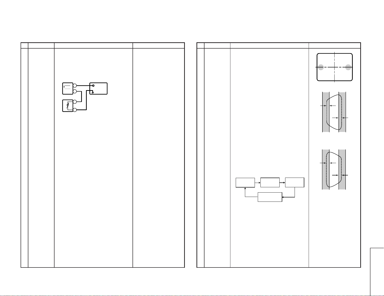
SERVICING OF HIGH VOLTAGE SYSTEM AND
PICTURETUBE
When servicing the high voltage system, remove static charge from it by
connecting a 10k ohm Resistor in series with an insulated wire (such as a
test probe) between picture tube dag and 2nd anode lead. (AC line cord
should be disconnected from AC outlet.)
1. Picture tube in this receiver employs integral implosion protection.
2. Replace with tube of the same type number for continued safety.
3. Do not lift picture tube by the neck.
4. Handle the picture tube only when wearing shatterproof goggles and after discharging
the high voltage completely.
X-RAY
This receiver is designed so that any X-Ray radiation is kept to an absolute
minimum. Since certain malfunctions or servicing may produce potentially
hazardous radiation with prolonged exposure at close range, the following
precautions should be observed:
1. When repairing the circuit,be sure not to increase the high voltage to more than 29.0 kV
(at beam 0 µA) for the set.
2. To keep the set in a normal operation, be sure to make it function on 24.8 ± 1.5 kV (at
beam 1,100 µA) in the case of the set. The set has been factory – Adjusted to the above-
mentioned high voltage.
∴If there is a possibility that the high voltage fluctuates as a result of the repairs,never
forget to check for such high voltage after the work.
3. Do not substitute a picture tube with unauthorized types and/or brands which may cause
excess X-ray radiation.
BEFORE RETURNINGTHE RECEIVER
Before returning the receiver to the user, perform the following safety
checks.
1. Inspect all lead dress to make certain that leads are not pinched or that hardware is not
lodged between the chassis and other metal parts in the receiver.
2. Inspect all protective devices such as non-metallic control knobs,insulating fishpapers,
cabinet backs, adjustment and compartment covers or shields, isolation resistor-
capacity networks, mechanical insulators etc.

3
3-1 3-2
CX51TXZ
ADJUSTMENT PRECAUTION
This model’s setting are adjusted in two different ways: though the I2C bus control and in the conventional analog
manner.The adjustments via the I2C bus control include preset-only items and variable data.
1. Setting the service mode by the microprocessor.
1Short TP1001 and TP1002 to switch to the service mode position, and the microprocessor is in input
mode. (Adjustment through the I2C bus control).(Use JWS Key to set as well).
2Press the CH DOWN / UP key on the remote controller to get ready to select the mode one by one.
3Press the CH DOWN / UP key on the remote controller to select the modes reversibly one by one.
4Using the VOLUME UP/ DOWN key on the remote controller, the data can be modified.
5Disconnect TP1001 and TP1002 to switch to the normal mode (OFF) position and the microprocessor is
in out of the service mode.
2. Factory Presetting.
1ShortTP1001 &TP1002 to switch to the service mode position and turn on the main power switch.Initial
values are automatically preset, only when a new EEPROM is used (Judge with the first 4 bytes).
2The initial data are preset as listed in pages 4-6.
3Make sure the data need modify or not (Initial data).
Note: Once the chassis has been assembly together and ready to be POWER ON for the FIRSTTIME, make
sure to short TP1001 and TP1002 to switch to the service mode position first and then turn on the
main power switch. (See 2-1above).
Precaution: If haven’t done this initiation, it may possibly generate excessive Beam current.
3. For reference please check with memory map (21SN Series type RH-IX3135CE Attachment)
■SERVICE MODE
(1) In the Service Mode, Key is used to select the mode in the following order.
FORWARD : CH DOWN key
REVERSE : CH UP key
FORWARD : CH DOWN key
REVERSE : CH UP key
STEP 2
STEP 1
R-CUT OFF
G-CUT OFF
B-CUT OFF
KEY
R-CUT OFF
G-CUT OFF
B-CUT OFF
G-DRIVE
B-DRIVE
UP
1 KEY
2 KEY
3 KEY
7 KEY
8 KEY
DOWN
4 KEY
5 KEY
6 KEY
F/B KEY
0 KEY
CUT-OFF/
BKGD mode
LATERAL mode
(R, G, B-CUT OFF)
G-DRIVE
B-DRIVE
CUT-OFF/BKGD mode
3-sec time out
-/-- KEY
3-sec time out
V-AMP 50 Hz (V-AMP50)
V-LINE 50 Hz (V-LINE50)
S-CORRECT 50 Hz (V S-CORR50)
V-PHASE 50 Hz (V-CENTER50)
H-PHASE 50 Hz (H-CENTER50)
SECAM R-Y (R-Y)
SECAM B-Y (B-Y)
50 Hz ADJUST mode COLOUR ADJUST mode
RASTER
mode CUT OFF
mode 50 Hz ADJUST
mode
60 Hz ADJUST
mode
NVM
SUB ADJ
mode COLOUR ADJUST
mode
MPX
ADJUST
OTHERS mode
MPX / STEP 2 SWITCH TO STEP 1 : LANG KEY (2 Sec)
Y-DL ADJUST mode
* ( ) means OSD display.

4
4-1 4-2
CX51TXZ
FORWARD : CH DOWN key
REVERSE : CH UP key
STEP 2
SUB BRIGHT (SUB BRI)
SUB COLOUR (SUB COL)
SUB TINT (SUB TINT)
V-AMP 60 Hz (V-AMP60)
V-LINE 60 Hz (V-LINE60)
V S-CORRECT 60Hz (V S-CORR60)
V-PHASE 60 Hz (V-CENTER60)
H-PHASE 60 Hz (H-CENTER60)
SUB ADJUST mode 60 Hz ADJUST mode
SUB SHARPNESS (SUB SHARP)
Y SUB CONTRAST (Y SUB CONT)
V-BLK START (V-BLK ST60)
V-BLK STOP (V-BLK SP60)
COLOUR PAL PARAMETER (COL PAL)
COLOUR SECAM PARAMETER
(COL SECAM)
COLOUR NTSC PARAMETER (COL NTSC)
N358 SHARPNESS (SHARP N358)
AV TINT PARAMETER (AV TINT)
AV SHARPNESS PARAMETER( AV SHARP)
ANR COLOUR STEP1 (ANR COL1)
ANR COLOUR STEP2 (ANR COL2)
ANR SHARPNESS STEP1 (ANR SHARP1)
ANR SHARPNESS STEP2 (ANR SHARP2)
* ( ) means OSD display.
Following MODES (STEP 2) can be switched by pressing LANG key (2 sec).
Press LANG Key for switch back STEP 1.
The data of STEP 2 is fixed, do not change without specific indication.
AGC SW (AGC)
AGC GAIN (GAIN)
WHITE TEMP (W.T.)
FM LEVEL (FM LV)
IGR LEVEL (IGR LV)
NICAM B/G LEVEL(B/G LV)
NICAM I LEVEL (I LV)
NICAM D/K LEVEL(D/K LV)
IGR GAIN (IGR)
LOWER ERROR (LOW ERR)
UPPER ERROR (UP ERR)
INTERNAL/EXTERNAL FM (FM)
AUTO MUTE (AM)
SUB CONTRAST (SUB CONT)
V-BLK STOP (V-BLK SP50)
V-BLK START (V-BLK ST50)
SEARCH SPEED (SEARCH)
AGC LEVEL (AGC LEVEL)
AGC SW (AGC SW)
BASS LEVEL (BASS LEVEL)
BASS SW (BASS SW)
Y-DELAY NTSC (DT NTSC M)
Y-DELAY SECAM (DT SECAM IDK)
Y-DELAY SECAM (DT SECAM BG)
Y-DELAY PAL (DT PAL IDK)
Y-DELAY PAL (DT PAL BG)
IC SELECTION (IC)
MODE USER DATA
CONTRAST MAX (64/64)
COLOUR CENT (32/64)
BRIGHTNESS CENT (32/64)
TINT CENT (32/64)
SHARPNESS CENT (32/64)
WHITE TEMP CENT (32/64)
S-VOLUME MIN (1/64)
BLUE BACK OFF
C SYSTEM AUTO
S SYSTEM *1
MODE KEY-IN KEY
H-CENTER* PICTURE
V-CENTER* TEXT
V-AMP* INDEX
V S CORR* RED
V-LINE* GREEN
SUB COLOUR TIMED PAGE
SUB BRIGHT SIZE
SUB TINT HOLD
R-Y YELLOW
B-Y CYAN
*1 : For each CH, before changing
service mode setting.
The flow of Mode lists as following,
* Direct Key-in Step1 Mode
PIN 31 PIN14 NICAM AV FAV. BIL C-SYS S-SYS AUTO
MODEL
B/G I D/K CH
SELECT
L L ON OFF OFF 2 ON OFF PSN ON OFF SN5
H L OFF ON OFF 2 OFF OFF PSN ON OFF SN8
L H ON ON ON 2 OFF OFF PSN ON OFF SN9
H H READ OUT EEPROM
INITIAL EEP ON OFF OFF 2 ON ON P OFF OFF FREE
While Pins (31), (14) of Micro are at H/H status in service mode, MENU Key can be used for setting data.
Check OSD display the model name, after the factory initial setting at CH1.
(A3HE51TXZ: Please confirm “SN5”, but no NICAM and IGR.)
USER DATA IN SERVICE MODE
* While SERVICE mode ON, EEPROM DATA will switch to the service data.
Also, once SERVICE mode OFF, EEPROM will switch back to previous USER DATA.
* In the service mode, the user data establish as below,
* Depend on reception signal 50/60 Hz.
OPTION INITIAL SETTING
Use the two ports of Micro for OPTION setting.

5
5-1 5-2
CX51TXZ
* After short TP1001 &TP1002, and turn on the MAIN Power Switch, read data from EEPROM Address 00H~03H,
and compare to the list below, if different, initialize the EEPROM.
Address: Data Address : Data
00H : 23H 02H : 13H
01H : 21H 03H : 85H
EEPROM item (OSD Display) Data length Initial data Remarks
(00H) –––––––––– 23H
(01H) –––––––––– 21H
(02H) –––––––––– 13H
(03H) –––––––––– 85H
R CUT OFF 0 ~ 255 0
G CUT OFF 0 ~ 255 0
B CUT OFF 0 ~ 255 0
G DRIVE 0 ~ 255 127
B DRIVE 0 ~ 255 127
50Hz V-AMP 0 ~ 127 58 +1 *1
50Hz V-LINEARITY 0 ~ 31 16 –2 *1
50Hz S CORRECTION 0 ~ 127 67 +7 *1 *2
50Hz V-PHASE 0 ~ 7 5 –3 *1
50Hz H-PHASE 0 ~ 31 7 +5 *1
60Hz V-AMP 0 ~ 127 59
60Hz V-LINEARITY 0 ~ 31 14
60Hz S CORRECTION 0 ~ 127 74 *2
60Hz V-PHASE 0 ~ 5 2
60Hz H-PHASE 0 ~ 31 12
SECAM R-Y 0 ~ 15 10
SECAM B-Y 0 ~ 15 6
SUB-BRIGHT 0 ~ 255 127
SUB-COLOUR 0 ~ 255 110
SUB-TINT 0 ~ 127 70
AFT/SKIP 0 ~ 1 ON/OFF
C-SYSTEM 0 ~ 1 AUTO
S-SYSTEM –––––––––– B/G
NVM When finish adjustments, DATA from 00H~03H differ from INITIAL DATA. Precaution, Once AC
Power ON, all DATA will be initiated.
MODE KEY-IN KEY
SEARCH SPEED REVEAL
COLOUR PAL RESET
Direct Key-in STEP 2 Mode
*1 : While 50 Hz mode has been adjusted, 60Hz mode’s data automatically will be input.
(But, while 60Hz mode has been adjusted, 50Hz mode’s data won’t be updated.)
*2 : Fixed DATA, do not change without specific indication.
STEP 2 IN SERVICE MODE
(Press LANG Key 2 seconds to switch from STEP 1)
Fixed DATA, do not change with out specific indication.
EEPROM item (OSD Display) Data adjustable range Data initial value Remarks
AGC SW ON
AGC GAIN 0
WT HI (LO*)
FM LEVEL 0dB
IGR LEVEL +2dB
NICAM B/G LEVEL –1dB
NICAM I LEVEL +4dB
NICAM D/K LEVEL –1dB
LOWER ERROR 35
UPPER ERROR 70
IGR GAIN (TDA9873H) 0
INTERNAL/EXTERNAL FM INTERNAL
AUTO MUTE ON
IC SELECT PH
Y-DELAY PAL B/G 2
Y-DELAY PAL IDK 2
Y-DELAY SECAM BG 4
Y-DELAY SECAM IDK 4
Y-DELAY NTSC M 2
BASS SW OFF
BASS LEVEL 0
AGC SW ON
AGC LEVEL 3
SEARCH SPEED 550
V-BLK ST50 0 ~ 63 63
V-BLK SP50 0 ~ 127 25
SUB CONTRAST 0 ~ 255 255
SUB SHARPNESS 0 ~ 63 28
Y SUB CONTRAST 0 ~ 31 18
V-BLK ST60 0 ~ 63 63
V-BLK SP60 0 ~ 127 20
COLOUR PAL PARAMETER +20
COLOUR SECAM PARAMETER +10
COLOUR NTSC PARAMETER +20
N358 SHARPNESS +10
AV TINT PARAMETER +3
AV SHARPNESS PARAMETER 0
ANR COLOUR STEP1 5
ANR COLOUR STEP2 10
ANR SHARPNESS STEP1 7
ANR SHARPNESS STEP2 12
EEPROM ITEMS' OSD DISPLAY JUDGE → WT
INITIAL DATA LOW → Hi
* “WT” (WHITE TEMP.LIMIT) follows Pin (29) of IC1001
WT Pin (29) of IC1001 OSD
HI L 5

6
6-1 6-2
CX51TXZ
INITIAL SETTING
(1) In service mode, After execute select POS 1, setting the following data in EEPROM.
MCL1
CH-NO Fv (MHz) Sound SYS
1 48.25 B/G
2 62.25 B/G
3 77.25 D/K
4 175.25 B/G
5 182.25 B/G
6 183.25 D/K
7 191.25 D/K
8 196.25 B/G
9 199.25 M
10 210.25 B/G
11 224.25 B/G
12 471.25 B/G
13 487.25 I
14 503.25 B/G
15 575.25 B/G
16 583.25 B/G
17 599.25 B/G
18 621.25 M
19 639.25 D/K
20 703.25 B/G
21 735.25 I
22 767.25 B/G
23 815.25 B/G
24 855.25 I
25 855.25 B/G
26 55.25 M
27 83.25 M
28 183.25 M
29 193.25 M
30 217.25 M
31 471.25 M
32 477.25 M
33 693.25 M
34 885.25 M
35 112.25 B/G
36 168.25 B/G
37
38 294.25 B/G
39 463.25 B/G
40
41 647.25 B/G
42 663.25 B/G
43 679.25 B/G
44 174.95 B/G
45 175.55 B/G
MCL2
CH-NO Fv (MHz) Sound SYS
1 46.25 B/G
2 64.25 B/G
3 86.25 B/G
4 95.25 B/G
5 138.25 B/G
6 175.25 B/G
7 182.25 B/G
8 189.25 B/G
9 196.25 B/G
10 209.25 B/G
11 216.25 B/G
12
13
14
15
16
17
18 527.25 B/G
19 847.25 B/G
20 48.25 B/G
21 175.25 B/G
22 210.25 B/G
23 224.25 B/G
24 575.25 B/G
25 599.25 B/G
26 767.25 B/G
27 183.25 M
28 193.25 M
29 112.25 B/G
30 168.25 B/G
31
32 294.25 B/G
33 463.25 B/G
34 174.25 B/G
35 175.25 B/G
36
37
38
39
38
41
42
43
44
45
Items Data Setting
SKIP OFF
AFT ON
C-SYSTEM AUTO
S-SYSTEM *1
LAST POWER ON
LAST TV/AV TV
DIGIT 1DIG
LANGUAGE *1
BLUE BACK ON
LAST POS 1
LAST FB POS 1
VOLUME MIN
CONTRAST MAX
COLOUR CENT
BRIGHTNESS CENT
TINT CENT
SHARPNESS CENT
WHITE TEMP CENT
BASS/TRE/BAL CENT
SPATIALIZER OFF
SPAT. LEVEL CENT
P-NR AUTO(TV)/OFF (AV)
SHIPPING SETTING AND CHECKING
(1) Just before pack the set, input setting, according to factory Initial setting 1~6 in EEPROM as below.
*1: Refer to M/M.
S-SYSTEM and LANGUAGE can be set to factory initial setting 1~6 at all CH.
FACTORY INITIAL SETTING LANGUAGE S- SYSTEM
1 CHINESE D/K
2 CHINESE I
3 ENGLISH B/G
4 ARABIC B/G
5 RUSSIAN D/K
6 MALAY B/G
MODEL OSD
A3HE21SN5C SN5
A3HE51TXZ
MODEL Magnetic Field (H,V) nT Background Lang. S-SYS Lang. QTY
Z 20,000 –50,000 12300K ENGLISH B/G 5
(2) Check OSD display the model name, after the factory initial setting at CH1.
MODEL CLASSIFIED FACTORY SETTING/MAGNETIC FILED (REFERENCE)

7
7-1 7-2
CX51TXZ
RF-AGC
check cut in
adjustment
(PRE SETTED)
1. Receive “PAL COLOUR BAR” signal.
»Signal Strength: 54 ± 1 dBµV (75 ohm open)
2. Connect the oscilloscope to TP210 (Tuner’s AGC
Terminal) as shown in
Fig. 1
.
3. DropInputSignalstrength to 51 ±1dBµV(75ohm
open).
4. Under 1. and 3. conditions, the output voltage
should be no change or below +0.1V.In addition,
change input signal strength to 57 ±2 dBµV, the
output voltage should be no less than -0.1V.
5. Change the antenna input signal to 63~67 dBµV,
and make sure there is no noise.
6. Turn uptheinputsignalto90~95dBµV to be sure
that there is no cross modulation beat.
Note: For the 50 ohm signal
strength gauge, when not
using 50/75 impedance
adapter,signalstrength is
52 ±1 dBµV (50 ohm
open), instead of 54 ±1
dBµV (75 ohm open).
precaution: The loss of
usingimpedance adapter.
»Bias box: About 4.5 V
Oscilloscope
0.1V
TV Set
Bias box
TP210+
+
–
–
Fig. 1
PIF ADJUSTMENT
No. Adjusting point Adjusting procedure/conditions Waveform and others
1
PURITY ADJUSTMENT
No. Adjusting point Adjusting procedure/conditions Waveform and others
Purity
adjustment 1. Receive the GREEN-ONLY signal. Adjust the
contrast control to have a beam current to
700 µA.
2. DegausstheCRTenoughwith the degausingcoil.
Note: Follow the Job Instruction Sheet to ad-
just the magnetic field.
Vertical Bv : -0.050 mT (-0.50 gauss)
Horizontal Bh: +0.020 mT (0.20 gauss)
(See page 12.)
3. Maintain the purity magnet at the zero magnetic
field and keep the static convergence roughly
adjusted.
4. Observe the points “a” and “b” as shown in
Fig.
2-1
through the microscope. Adjust the landings
to “A” rank requirements.
5. Orient the raster rotation to 0 eastward.
6. Tighten up the deflection coil screws.
»Tightening torque: 108 ± 20 N (11 ± 2 kgf)
7. Make sure the CRT corners landing meet the “A”
rank requirements.If not, stick the magnet sheet
to correct it.
Note: This adjustment must be done after
warming up the unit for 30 minutes or
longer with a beam current over 700 µA.
Note: Set the service mode by TP1001 and
TP1002 (short) then press factory proc-
ess R/C RGB key to change to RGB
mono colour mode.
* For the following colours press R/C RGB key to
change.
1
* Press R/C RGB key for 1 sec-
ond in NORMAL MODE, the
colourwillchange toRGBmono
colour mode.
The TEXT Key “R. G. Cy” Key
can be directly use to change
to other colours screen.
Green-only Blue-only Red-only
redish Absolved
ab
A
B
A
B
A = B
A = B
Rank "A"
(on the right of the CRT)
Rank "A"
(on the left of the CRT)
Fig. 2-1
Fig. 2-2
Fig. 2-3

8
8-1 8-2
CX51TXZ
CONVERGENCE ADJUSTMENT
No. Adjusting point Adjusting procedure/conditions Waveform and others
Convergence
adjustment
(to be done
after the purity
adjustment)
1. Receive the “Crosshatch Pattern” signal.
2. Using the remote controller, call NORMAL mode.
STATIC CONVERGENCE
1. Turn the 4-pole magnet to a proper opening an-
gle in order to superpose the blue and red col-
ours.
2. Turn the 6-pole magnet to a proper opening an-
gle in order to superpose the green colour over
the blue and red colours.
DYNAMIC CONVERGENCE
1. Adjust the convergence on the fringes of the
screen in the following steps.
a)
Fig. 3-1
: Drive the wedge at point “a” and
swing the deflection coil upward.
b)
Fig. 3-2
: Drive the wedge at points “b” and
“c”and swing the deflection coil downward.
c)
Fig. 3-3
: Drive the “c” wedge deeper and
swing the deflection coil rightward.
d)Fig. 3-4: Drive the “b” wedge deeper and
swing the deflection coil leftward.
2. Fix all the wedges on the CRT and apply glass
tape over them.
3. Apply lacquer to the deflection yoke lock screw,
magnet unit (purity, 4-pole, 6-pole magnets) and
magnet unit lock screw.
Finally received the Red-only and Blue-only sig-
nalstomakesure there is no other colours on the
screen.
1
RGB
BGR
R
G
B
R
G
B
B
G
R
B
G
R
RGB
BGR
Fig. 3-2
Fig. 3-1
Fig. 3-3
Fig. 3-4
Fig. 3-5
Fig. 3-6
Lacquer
Wedge "a"
Wedge
"b" Wedge
"c"
About
100°
About
100°
4-pole magnet
6-pole magnet
CRT neck
20mm
Lacquer
Purity magnet
CRT CUT-OFF, BACKGROUND AND SUB-CONTRAST ADJUSTMENT
No. Adjusting point Adjusting procedure/conditions Waveform and others
CRT cut-off
adjustment
I2C bus
Control
adjustment
1. Receive the the “Monoscope Pattern” signal.
2. Press R/C to set Picture in Normal condition.
3. Call the Service mode and select the “Cut-off/
Background” mode.
4. Set the screen control to 0 / 10 position.
5. Press “-/--” key on the remote controller to reach
the horizontal centering mode.
6. Hereoneofthe three colourwillappear as abright
line when the screen controlis turned clockwise.
Adjust the screen VR until the line can be seen
slightly on the screen.
7. Use the control key in the R/C to adjust the quan-
tity of the other two colours, thus touching off the
bias control belonging to the first colour, until the
horizontal raster becomes white.
8. Turn off the screen control (counter-clockwise)
until the horizontal raster disappears.
Note: Before starting this adjustment ,warm
up the unit for 30 minutes or longer at
a beam current of over 700 µA.
9. Press the “-/--” key on the remote control to call
the NORMAL mode.
10
.Call“SUB-BRIGHT”inSERVICE mode.(Receive
Crosshatch Signal with 5 black level window)
11
.Adjust the “SUB BRIGHT” bus data in order that
the line 1, 2 and 3 have the same darkness
wherelse line 4 is slightly brighter than line 1, 2
and 3 and finally line 5 will be the brighter than
line 4.
12
.The rangeofthe“SUBBRIGHT”mustbe between
107and157(127 +30, –20).(Ifthe“SUBBRIGHT”
is out of the range as mention above, please do
adjust from step 1. to 11. again.)
Note: Steps 10. and 11. should be adjusted af-
ter WHITE BALANCE ADJUSTMENT.
For the “SUB BRIGHT” out of range
mention above, it will result in the dif-
ferent brightness of OSD.
1* Before adjustment , make sure
thatthis adjustmentwith the ini-
tial bus data
“R-CUT OFF”, “G-CUT OFF”,
“B-CUT OFF”, “B-DRIVE” &
“G-DRIVE”.
Note:
R CUT OFF UP “1” KEY
DOWN “4” KEY
G CUT OFF UP “2” KEY
DOWN “5” KEY
B CUT OFF UP “3” KEY
DOWN “6” KEY
The data can be turned up
and down with the above
keys.
Make sure all the 1st, 2nd and
3rd black portions are at the
same black level.
1 2 3 4 5

9
9-1 9-2
CX51TXZ
CRT CUT-OFF, BACKGROUND AND SUB-CONTRAST ADJUSTMENT
(Continued)
No. Adjusting point Adjusting procedure/conditions Waveform and others
White balance
Service mode
adjustment
I2C bus
control
adjustment
1. Receive the “Monoscope Pattern” signal.
2. Press R/C to set Picture NORMAL condition.
3. Connect the DC miliammeter between TP602 (–)
and TP603 (+).
4. Check Beam current should be around 1,100 µA.
5. Set it to service mode and adjust the “G-DRIVE”,
“B-DRIVE” data to have a colour temperature of
12,300°K.
6. Whenchangedbackto non-servicemode,adjust
theContrast&Brightnesscontroltohaveabeam
current of 200µA.If the colour temperature is not
at 12,300°K go back to No. 1.
Note: This adjustment must be done after
warming up the unit for 30 minutes or
longer with a beam current over 700 µA.
2Refer to Page 6.
* 12300°K X: 0.272
Y: 0.275
(with colour temperature meter
CA-100 (MINOLTA).)
Note:
G-DRIVE UP “7” KEY
DOWN “F/B” KEY
B-DRIVE UP “8” KEY
DOWN “0” KEY
The data can be turned up
and down with the above
keys.
Maximum
beam check 1. Receive the “Monoscope Pattern” signal.
2. Press R/C to set Picture NORMAL condition.
3. Connect the DC miliammeter between TP603 (+)
and TP602 (–).
(Full Scale: 3 mA Range)
4. Beam current must be within 1,100 ± 100 µA.
3
HORIZONTAL AND VERTICAL DEFLECTION LOOP ADJUSTMENT
No. Adjusting point Adjusting procedure/conditions Waveform and others
V-AMP 50
V-LINEARITY-
50 Hz
V-S
CORRECTION-
50 Hz
V-SHIFT 50
(V-CENTER)
H-SHIFT (50)
(H-CENTER)
1. AdjustV-AMP50 to set overscan of 9.5% typical.
(“Monoscope Pattern” signal (50Hz))
Adjustment Spec 9.5% range +1% –0%.
1. Adjust V-LIN to have the best vertical linearity.
1. Pre-set, NO NEED adjust. (Only if can’t meet the
specification (±10%) of vertical linearity, then ad-
just V-SCORRECTION.)
1. Align the pattern’s center with the CRT mechani-
cal center.
1. Adjust H-SHIFT until left and right overscan is
same.
ForV-AMP 60,V-LINEARITY 60,V-SCORRECTION
60, V-SHIFT 60 (Data Range “0”~“5”), H-SHIFT 60,
while 50 Hz mode has been adjusted automatically
data will be input.
* Please check the 60 Hz and re-adjust if there is
necessary to adjust. Please check also the PAL
60 Hz in dark condition wether left side of the
screen got blank or not and re-adjust when it hap-
pen.
1( ) Mean reception channel
Focus
adjustment 1. Receive the “Monoscope Pattern” signal.
2. Press R/C to set Picture NORMAL condition.
3. Adjust the focus control so that the screen be in
good focus.
2

10
10-1 10-2
CX51TXZ
PAL CHROMA ADJUSTMENT
No. Adjusting point Adjusting procedure/conditions Waveform and others
Sub-colour
I2C bus
adjustment
1. Receive the “PAL Colour Bar” signal.
2. Press R/C to set Picture Normal condition.
3. ConnecttheoscilloscopetoTP852(Redcathode).
»Range :20V/div.(AC) (Using 10:1 probe)
»Sweep time : 10 µsec/div.
4. UsingtheR/Ccall“SUB COL”inSERVICEmode.
Adjust SUB COLOUR bus data, so that the 75%
White & Red portions of PAL Colour Bar be at the
same level shown as
Fig. 4
.
5. Clear the SERVICE mode.
1
NTSC CHROMA ADJUSTMENT
No. Adjusting point Adjusting procedure/conditions Waveform and others
Sub-tint
I2C bus
adjustment
1. Receive the “NTSC3.58 Colour Bar” signal for
SUB-TINT adjustment.
2. Connect the oscilloscope to TP801 (Pin (36) of
IC801 (B-Y)).
»Range :100mV/div.(AC)(UseProbe10:1)
»Sweep time : 10 µsec/div.
3. Call the “SUB-TINT” mode in service mode. Ad-
just the “SUB-TINT”bus data to obtain the wave-
form shown as
Fig. 5
.
4. Clear the SERVICE mode.
1
Cy GB
WY 100%W
75%
Fig. 4
Mg R
WYCy G Mg R B
Fig. 5
A=B=C
(B–Y)
A
B
C
SECAM CHROMA ADJUSTMENT
No. Adjusting point Adjusting procedure/conditions Waveform and others
SECAM black
level
(R-Y/B-Y)
I2C bus
adjustment
1. Receive “SECAM COLOUR BAR”signal.
2. SetSECAMblackleveladjustment intoR-Ymode.
3. ConnectoscilloscopetoTP802(Pin(35) of IC801
(R-Y out)).
»Range :100 mV/div.(AC)(Use 10:1 Probe)
»Sweep time : 10 µsec/div.
4. Adjust the offset of R-Y to minimum, shown in
Fig. 6-1 (b)
.
Adjust the offset of between no-signal line and
signal line be minimum.
5. Call the SECAM black level adjustment into B-Y
mode.
6. Connect again oscilloscope toTP801 (Pin (36) of
IC801 (B-Y out)) with the similar condition as (3).
7. Adjusttheoffsetof B-Y to minimum,shown in
Fig.
6-2 (b)
.
Adjust the offset of between no-signal line and
signal line be minimum.
1
OFF SET
OFF SET
Fig. 6-1 (a)
Fig. 6-1 (b)
Fig. 6-2 (a)
Fig. 6-2 (b)

11
11-1 11-2
CX51TXZ
PROTECTOR PERFORMANCE CHECK
No. Adjusting point Adjusting procedure/conditions Waveform and others
Beam
protector 1. Receive “Monoscope Pattern” signal.
2. Set the contrast control to maximum.
3. Set the brightness control to maximum.
4. Make a short circuit between the collector and
emitter of Q851, Q852 or Q853 and make sure
that the protector is activated and the stand-by
mode is called.
1* Short-circuit any of the Q851,
Q852 and Q853.
High-voltage
protector 1. Receive “Monoscope Pattern” signal.
2. Connect output of Bias Box to D607 cathode
(R635 side).
3. Set voltage of Bias Box to 18V and make sure
the protector is not work.
4. Set voltage of Bias Box to 27V, and make sure
the protector is work.
2
Other
protectors 1. Once finish rectified Electrolytic Capacitor short
testing in +B line, check all possible damaged
components on +B line.
(Use random selected set for inspection)
3
A/V INPUT AND OUTPUT CHECK
No. Adjusting point Adjusting procedure/conditions Waveform and others
Video and
audio output
check
1. Receivethe“PALColourBar”signal(100%White
Colour Bar, 400 Hz 100% modulation audio (±50
kHz Dev)
2. Terminate theVideo output with a 75 ohm imped-
ance.Make sure the output is as specified (1.0
Vp-p ±3 dB).
3. Terminate the Audio output with a 10k ohm im-
pedance. Make sure the output is as specified
(1.76 Vp-p ±3 dB).
1
Video and
audio input
check
1. Using the TV/AV key on the remote controller,
make sure that the modes change in the order of
TV, AV1, AV2 and TV again and that the video
and audio outputs are according to the input ter-
minal for each mode.
2
FUNCTION OPERATION CHECKING (VIDEO AND AUDIO)
No. Adjusting point Adjusting procedure/conditions Waveform and others
CONTRAST
key 1. Receive “Monoscope Pattern” signal.
2. Select the Contrast on the P-MODE screen.
3. PressVolume Up/Down keyto checkwhetherthe
contrast effect is OK or not.
1
COLOUR key 1. Receive “Colour Bar” signal.
2. Select the Colour on the P-MODE screen.
3. PressVolume Up/Down keyto checkwhetherthe
colour effect is OK or not.
2
BRIGHTNESS
key 1. Receive “Monoscope Pattern” signal.
2. Select the Brightness on the P-MODE screen.
3. PressVolume Up/Down keyto checkwhetherthe
Brightness effect is OK or not.
3
TINT key 1. Receive the “NTSC Colour Bar” signal.
2. Select the Tint on the P-MODE screen.
3. PressVolume Up/Down key to checkTint, Up for
green direction and down for purple direction
whether is OK or not.
4
NORMAL key 1. Once in PICTURE-Mode when the NORMAL key
is pressed, all the settings will be present to nor-
mal setting.
(Normal setting value for every mode).
»Contrast : MAX
»Colour : CENTER
»Brightness : CENTER
»Tint : CENTER
»Sharpness : CENTER
»White Temp : CENTER
»Auto NR : AUTO (AV mode, NR off)
5 Note: Ifnothing isdisplaymean
contrast, colour, bright, tint,
sharpness are all in normal
setting.

12
12-1 12-2
CX51TXZ
FUNCTION OPERATION CHECKING (VIDEO AND AUDIO)
(Continued)
No. Adjusting point Adjusting procedure/conditions Waveform and others
WHITETEMP 1. Receive “Monoscope Pattern” signal.
2. Select the White temp on the P-MODE screen.
3. Press Volume Up/Down key to check WHITE
TEMP, UP for more bluish direction changing,
DOWN for more reddish direction changing.
8
SHARPNESS
key 1. Receive “Monoscope Pattern” signal.
2. Select the Sharpness on the P-MODE screen.
3. PressVolume Up/Down keyto checkwhetherthe
Sharpness effect is OK or not.
6
CH display
colour 1. All the channel (1~99) will have an OSD display
ofthechannelnumberin green colour under AFT
ON condition.
7
COLOUR
SYSTEM 1. Receive the “PAL COLOUR BAR” signal, press
the COLOUR SYSTEM key to select modes ex-
ceptPAL, checktheCOLOURis notworkingprop-
erly.
Then, select the“PAL” mode.Check again its col-
our so that it is working properly.
2. Receive “SECAM COLOUR BAR” signal, press
COLOUR SYSTEM key to select modes except
SECAM,checkthe COLOUR isnotworkingprop-
erly.
Then, select the“SECAM” mode.Check again its
colour so that it is working properly.
3. Receive“NTSC4.43COLOUR BAR”signal, press
COLOUR SYSTEM key to select modes except
N4.43, check the COLOUR is not working prop-
erly. Then, select the “NTSC 4.43” mode. Check
again its colour so that it is working properly.
4. Receive“NTSC3.58COLOUR BAR”signal, press
COLOUR SYSTEM key to select modes except
N3.58, check the COLOUR is not working prop-
erly. Then, select the “NTSC 3.58” mode. Check
again its colour so that it is working properly.
9
FUNCTION OPERATION CHECKING (VIDEO AND AUDIO)
(Continued)
No. Adjusting point Adjusting procedure/conditions Waveform and others
SOUND
SYSTEM 1. Receive “PAL-D/K” signal, press the “SOUND
SYSTEM” to select B/G, I, M. Check the sound
output is not working properly.
Select D/K and check the sound output to make
sure it is working properly.
2. Receive “PAL-I” signal, press the “SOUND SYS-
TEM” to select B/G, D/K, M. Check the sound
output is not working properly.
SelectIandcheck the sound outputtomakesure
it is working properly.
3. Receive “PAL-B/G” signal, press the “SOUND
SYSTEM” to select I, D/K, M. Check the sound
output is not working properly.
Select B/G and check the sound output to make
sure it is working properly.
4. Receive “NTSC-M” signal, press the “SOUND
SYSTEM” to select B/G, D/K, I, check the sound
output is not working properly.
Select M and check the sound output to make
sure it is working properly.
10
Noise mute
checking 1. Receive “PAL COLOUR BAR” signal.
2. Turn up the volume control to maximum, make
sure the sound is heard from the speakers.Then
put the unit in no signal state.
3. Check the sound mute is effective.
4. Finally turn down the sound volume to minimum.
11

13
13-1 13-2
CX51TXZ
FUNCTION OPERATION CHECKING (VIDEO AND AUDIO)
(Continued)
No. Adjusting point Adjusting procedure/conditions Waveform and others
Other
(NICAM/IGR/
TEXT/FAV. CH)
1. Check Normal operation of each model of differ-
ent features.
12
OSD
Language
quantity check
1. Check OSD LANGUAGE quantity.13
Model NICAM IGR TEXT FAV. CH
CX51TXZ X X O O
Model Quantity English Russian Chinese French Arabic Malay
CX51TXZ 5 O X O O O O
SUB
ADDRESS
DATA FACTORY
SETTING
REMARKS CRITERIA
76543210
000 PASS WORD “23“ 23OUTSIDE $23
001 PASS WORD “21“ 21OUTSIDE $21
002 PASS WORD “13“ 13OUTSIDE $13
003 PASS WORD “85“ 85OUTSIDE $85
004 PLL DATA (Higher rank) CH0
005 PLL DATA (Lower rank)
006 PLL DATA (Higher rank) CH1
007 PLL DATA (Lower rank)
008 PLL DATA (Higher rank) CH2
009 PLL DATA (Lower rank)
00A PLL DATA (Higher rank) CH3
00B PLL DATA (Lower rank)
00C PLL DATA (Higher rank) CH4
00D PLL DATA (Lower rank)
00E PLL DATA (Higher rank) CH5
00F PLL DATA (Lower rank)
010 PLL DATA (Higher rank) CH6
011 PLL DATA (Lower rank)
012 PLL DATA (Higher rank) CH7
013 PLL DATA (Lower rank)
014 PLL DATA (Higher rank) CH8
015 PLL DATA (Lower rank)
016 PLL DATA (Higher rank) CH9
017 PLL DATA (Lower rank)
018 PLL DATA (Higher rank) CH10
019 PLL DATA (Lower rank)
01A PLL DATA (Higher rank) CH11
01B PLL DATA (Lower rank)
01C PLL DATA (Higher rank) CH12
01D PLL DATA (Lower rank)
01E PLL DATA (Higher rank) CH13
01F PLL DATA (Lower rank)
020 PLL DATA (Higher rank) CH14
021 PLL DATA (Lower rank)
022 PLL DATA (Higher rank) CH15
023 PLL DATA (Lower rank)
024 PLL DATA (Higher rank) CH16
025 PLL DATA (Lower rank)
026 PLL DATA (Higher rank) CH17
027 PLL DATA (Lower rank)
028 PLL DATA (Higher rank) CH18
029 PLL DATA (Lower rank)
02A PLL DATA (Higher rank) CH19
02B PLL DATA (Lower rank)
02C PLL DATA (Higher rank) CH20
02D PLL DATA (Lower rank)
02E PLL DATA (Higher rank) CH21
02F PLL DATA (Lower rank)
MEMORY MAP

14
14-1 14-2
CX51TXZ
030 PLL DATA (Higher rank) CH22
031 PLL DATA (Lower rank)
032 PLL DATA (Higher rank) CH23
033 PLL DATA (Lower rank)
034 PLL DATA (Higher rank) CH24
035 PLL DATA (Lower rank)
036 PLL DATA (Higher rank) CH25
037 PLL DATA (Lower rank)
038 PLL DATA (Higher rank) CH26
039 PLL DATA (Lower rank)
03A PLL DATA (Higher rank) CH27
03B PLL DATA (Lower rank)
03C PLL DATA (Higher rank) CH28
03D PLL DATA (Lower rank)
03E PLL DATA (Higher rank) CH29
03F PLL DATA (Lower rank)
040 PLL DATA (Higher rank) CH30
041 PLL DATA (Lower rank)
042 PLL DATA (Higher rank) CH31
043 PLL DATA (Lower rank)
044 PLL DATA (Higher rank) CH32
045 PLL DATA (Lower rank)
046 PLL DATA (Higher rank) CH33
047 PLL DATA (Lower rank)
048 PLL DATA (Higher rank) CH34
049 PLL DATA (Lower rank)
04A PLL DATA (Higher rank) CH35
04B PLL DATA (Lower rank)
04C PLL DATA (Higher rank) CH36
04D PLL DATA (Lower rank)
04E PLL DATA (Higher rank) CH37
04F PLL DATA (Lower rank)
050 PLL DATA (Higher rank) CH38
051 PLL DATA (Lower rank)
052 PLL DATA (Higher rank) CH39
053 PLL DATA (Lower rank)
054 PLL DATA (Higher rank) CH40
055 PLL DATA (Lower rank)
056 PLL DATA (Higher rank) CH41
057 PLL DATA (Lower rank)
058 PLL DATA (Higher rank) CH42
059 PLL DATA (Lower rank)
05A PLL DATA (Higher rank) CH43
05B PLL DATA (Lower rank)
05C PLL DATA (Higher rank) CH44
05D PLL DATA (Lower rank)
05E PLL DATA (Higher rank) CH45
05F PLL DATA (Lower rank)
SUB
ADDRESS
DATA FACTORY
SETTING
REMARKS CRITERIA
76543210 060 PLL DATA (Higher rank) CH46
061 PLL DATA (Lower rank)
062 PLL DATA (Higher rank) CH47
063 PLL DATA (Lower rank)
064 PLL DATA (Higher rank) CH48
065 PLL DATA (Lower rank)
066 PLL DATA (Higher rank) CH49
067 PLL DATA (Lower rank)
068 PLL DATA (Higher rank) CH50
069 PLL DATA (Lower rank)
06A PLL DATA (Higher rank) CH51
06B PLL DATA (Lower rank)
06C PLL DATA (Higher rank) CH52
06D PLL DATA (Lower rank)
06E PLL DATA (Higher rank) CH53
06F PLL DATA (Lower rank)
070 PLL DATA (Higher rank) CH54
071 PLL DATA (Lower rank)
072 PLL DATA (Higher rank) CH55
073 PLL DATA (Lower rank)
074 PLL DATA (Higher rank) Ch56
075 PLL DATA (Lower rank)
076 PLL DATA (Higher rank) CH57
077 PLL DATA (Lower rank)
078 PLL DATA (Higher rank) CH58
079 PLL DATA (Lower rank)
07A PLL DATA (Higher rank) CH59
07B PLL DATA (Lower rank)
07C PLL DATA (Higher rank) Ch60
07D PLL DATA (Lower rank)
07E PLL DATA (Higher rank) CH61
07F PLL DATA (Lower rank)
080 PLL DATA (Higher rank) CH62
081 PLL DATA (Lower rank)
082 PLL DATA (Higher rank) CH63
083 PLL DATA (Lower rank)
084 PLL DATA (Higher rank) CH64
085 PLL DATA (Lower rank)
086 PLL DATA (Higher rank) CH65
087 PLL DATA (Lower rank)
088 PLL DATA (Higher rank) CH66
089 PLL DATA (Lower rank)
08A PLL DATA (Higher rank) CH67
08B PLL DATA (Lower rank)
08C PLL DATA (Higher rank) CH68
08D PLL DATA (Lower rank)
08E PLL DATA (Higher rank) CH69
08F PLL DATA (Lower rank)
SUB
ADDRESS
DATA FACTORY
SETTING
REMARKS CRITERIA
76543210

15
15-1 15-2
CX51TXZ
090 PLL DATA (Higher rank) CH70
091 PLL DATA (Lower rank)
092 PLL DATA (Higher rank) CH71
093 PLL DATA (Lower rank)
094 PLL DATA (Higher rank) CH72
095 PLL DATA (Lower rank)
096 PLL DATA (Higher rank) CH73
097 PLL DATA (Lower rank)
098 PLL DATA (Higher rank) CH74
099 PLL DATA (Lower rank)
09A PLL DATA (Higher rank) CH75
09B PLL DATA (Lower rank)
09C PLL DATA (Higher rank) CH76
09D PLL DATA (Lower rank)
09E PLL DATA (Higher rank) CH77
09F PLL DATA (Lower rank)
0A0 PLL DATA (Higher rank) CH78
0A1 PLL DATA (Lower rank)
0A2 PLL DATA (Higher rank) CH79
0A3 PLL DATA (Lower rank)
0A4 PLL DATA (Higher rank) CH80
0A5 PLL DATA (Lower rank)
0A6 PLL DATA (Higher rank) CH81
0A7 PLL DATA (Lower rank)
0A8 PLL DATA (Higher rank) CH82
0A9 PLL DATA (Lower rank)
0AA PLL DATA (Higher rank) CH83
0AB PLL DATA (Lower rank)
0AC PLL DATA (Higher rank) CH84
0AD PLL DATA (Lower rank)
0AE PLL DATA (Higher rank) CH85
0AF PLL DATA (Lower rank)
0B0 PLL DATA (Higher rank) CH86
0B1 PLL DATA (Lower rank)
0B2 PLL DATA (Higher rank) CH87
0B3 PLL DATA (Lower rank)
0B4 PLL DATA (Higher rank) CH88
0B5 PLL DATA (Lower rank)
0B6 PLL DATA (Higher rank) CH89
0B7 PLL DATA (Lower rank)
0B8 PLL DATA (Higher rank) CH90
0B9 PLL DATA (Lower rank)
0BA PLL DATA (Higher rank) CH91
0BB PLL DATA (Lower rank)
0BC PLL DATA (Higher rank) CH92
0BD PLL DATA (Lower rank)
0BE PLL DATA (Higher rank) CH93
0BF PLL DATA (Lower rank)
SUB
ADDRESS
DATA FACTORY
SETTING
REMARKS CRITERIA
76543210
SUB
ADDRESS
DATA FACTORY
SETTING
REMARKS CRITERIA
76543210
0C0 PLL DATA (Higher rank) CH94
0C1 PLL DATA (Lower rank)
0C2 PLL DATA (Higher rank) CH95
0C3 PLL DATA (Lower rank)
0C4 PLL DATA (Higher rank) CH96
0C5 PLL DATA (Lower rank)
0C6 PLL DATA (Higher rank) CH97
0C7 PLL DATA (Lower rank)
0C8 PLL DATA (Higher rank) CH98
0C9 PLL DATA (Lower rank)
0CA PLL DATA (Higher rank) CH99
0CB PLL DATA (Lower rank)
0CC LAST POWER ON:AA OFF:55 AA
0CD BLUE BACK 1DIGIT/2DIGIT OFF/1DIG ON:A OFF:5 / 55
1DIG:5 2DIG:A
0CE AUTO SELECT LANGUAGE OFF/ENG ON:A OFF:5 / 50
E:0 R:1 C:2 A:3 F:4 M:5
0CF LAST POSITION POS1 01
0D0 LAST CONTRAST 60 3C
0D1 LAST COLOUR ±0 1E
0D2 LAST BRIGHT ±0 1E
0D3 LAST TINT ±0 1E
0D4 LAST SHARPNESS ±0 1E
0D5 LAST WHITE TEMP ±0 1E
0D6 NR(AV) NR(TV) OFF/AUTO
ON1:2 ON2:4 OFF:0 /
01
AUTO:1 OFF:0
0D7 LAST TREBLE ±0 1E
0D8 LAST BASS ±0 1E
0D9 LAST SPATIALIZER MODE OFF
ON1:1 ON2:2 OFF:0
00
0DA LAST SPATIALIZER LEVEL ±0 1E
0DB LAST BALANCE ±0 1E
0DC LAST VOLUME 0 00
0DD ON TIMER VOLUME UNINSTAL FF
0DE LAST SERVICE MODE SERVICE 00
0DF LAST TV/AV MODE TV TV:1 AV1:1 AV2:2 00
0E0 CH7 CH6 CH5 CH4 CH3 CH2 CH1 CH0 AFT FF
0E1 CH15 CH14 CH13 CH12 CH11 CH10 CH9 CH8 0 : OFF FF
0E2 CH23 CH22 CH21 CH20 CH19 CH18 CH17 CH16 1 : ON FF
0E3 CH31 CH30 CH29 CH28 CH27 CH26 CH25 CH24 FF
0E4 CH39 CH38 CH37 CH36 CH35 CH34 CH33 CH32 FF
0E5 CH47 CH46 CH45 CH44 CH43 CH42 CH41 CH40 FF
0E6 CH55 CH54 CH53 CH52 CH51 CH50 CH49 CH48 FF
0E7 CH63 CH62 CH61 CH60 CH59 CH58 CH57 CH56 FF
0E8 CH71 CH70 CH69 CH68 CH67 CH66 CH65 CH64 FF
0E9 CH79 CH78 CH77 CH76 CH75 CH74 CH73 CH72 FF
0EA CH87 CH86 CH85 CH84 CH83 CH82 CH81 CH80 FF
0EB CH95 CH94 CH93 CH92 CH91 CH90 CH89 CH88 FF
0EC CH99 CH98 CH97 CH96 FF

16
16-1 16-2
CX51TXZ
0ED
0EE
0EF
0F0 CH7 CH6 CH5 CH4 CH3 CH2 CH1 CH0 SKIP 00
0F1 CH15 CH14 CH13 CH12 CH11 CH10 CH9 CH8 0 : OFF 00
0F2 CH23 CH22 CH21 CH20 CH19 CH18 CH17 CH16 1 : ON 00
0F3 CH31 CH30 CH29 CH28 CH27 CH26 CH25 CH24 00
0F4 CH39 CH38 CH37 CH36 CH35 CH34 CH33 CH32 00
0F5 CH47 CH46 CH45 CH44 CH43 CH42 CH41 CH40 00
0F6 CH55 CH54 CH53 CH52 CH51 CH50 CH49 CH48 00
0F7 CH63 CH62 CH61 CH60 CH59 CH58 CH57 CH56 00
0F8 CH71 CH70 CH69 CH68 CH67 CH66 CH65 CH64 00
0F9 CH79 CH78 CH77 CH76 CH75 CH74 CH73 CH72 00
0FA CH87 CH86 CH85 CH84 CH83 CH82 CH81 CH80 00
0FB CH95 CH94 CH93 CH92 CH91 CH90 CH89 CH88 00
0FC CH99 CH98 CH97 CH96 00
0FD
0FE
0FF
SUB
ADDRESS
DATA FACTORY
SETTING
REMARKS CRITERIA
76543210 100 S-SYSTEM C-SYSTEM CH0 B:0 I:1 D:2 M:3 / 00
AU:0 PA:1 SE:2 N4:3 N3:4
101 S-SYSTEM C-SYSTEM CH1 00
102 S-SYSTEM C-SYSTEM CH2 00
103 S-SYSTEM C-SYSTEM CH3 00
104 S-SYSTEM C-SYSTEM CH4 00
105 S-SYSTEM C-SYSTEM CH5 00
106 S-SYSTEM C-SYSTEM CH6 00
107 S-SYSTEM C-SYSTEM CH7 00
108 S-SYSTEM C-SYSTEM CH8 00
109 S-SYSTEM C-SYSTEM CH9 00
10A S-SYSTEM C-SYSTEM CH10 00
10B S-SYSTEM C-SYSTEM CH11 00
10C S-SYSTEM C-SYSTEM CH12 00
10D S-SYSTEM C-SYSTEM CH13 00
10E S-SYSTEM C-SYSTEM CH14 00
10F S-SYSTEM C-SYSTEM CH15 00
110 S-SYSTEM C-SYSTEM CH16 00
111 S-SYSTEM C-SYSTEM CH17 00
112 S-SYSTEM C-SYSTEM CH18 00
113 S-SYSTEM C-SYSTEM CH19 00
114 S-SYSTEM C-SYSTEM CH20 00
115 S-SYSTEM C-SYSTEM CH21 00
116 S-SYSTEM C-SYSTEM CH22 00
117 S-SYSTEM C-SYSTEM CH23 00
118 S-SYSTEM C-SYSTEM CH24 00
119 S-SYSTEM C-SYSTEM CH25 00
11A S-SYSTEM C-SYSTEM CH26 00
11B S-SYSTEM C-SYSTEM CH27 00
11C S-SYSTEM C-SYSTEM CH28 00
11D S-SYSTEM C-SYSTEM CH29 00
11E S-SYSTEM C-SYSTEM CH30 00
11F S-SYSTEM C-SYSTEM CH31 00
120 S-SYSTEM C-SYSTEM CH32 00
121 S-SYSTEM C-SYSTEM CH33 00
122 S-SYSTEM C-SYSTEM CH34 00
123 S-SYSTEM C-SYSTEM CH35 00
124 S-SYSTEM C-SYSTEM CH36 00
125 S-SYSTEM C-SYSTEM CH37 00
126 S-SYSTEM C-SYSTEM CH38 00
127 S-SYSTEM C-SYSTEM CH39 00
128 S-SYSTEM C-SYSTEM CH40 00
129 S-SYSTEM C-SYSTEM CH41 00
12A S-SYSTEM C-SYSTEM CH42 00
12B S-SYSTEM C-SYSTEM CH43 00
12C S-SYSTEM C-SYSTEM CH44 00
12D S-SYSTEM C-SYSTEM CH45 00
12E S-SYSTEM C-SYSTEM CH46 00
SUB
ADDRESS
DATA FACTORY
SETTING
REMARKS CRITERIA
76543210

17
17-1 17-2
CX51TXZ
12F S-SYSTEM C-SYSTEM CH47 00
130 S-SYSTEM C-SYSTEM CH48 00
131 S-SYSTEM C-SYSTEM CH49 00
132 S-SYSTEM C-SYSTEM CH50 00
133 S-SYSTEM C-SYSTEM CH51 00
134 S-SYSTEM C-SYSTEM CH52 00
135 S-SYSTEM C-SYSTEM CH53 00
136 S-SYSTEM C-SYSTEM CH54 00
137 S-SYSTEM C-SYSTEM CH55 00
138 S-SYSTEM C-SYSTEM CH56 00
139 S-SYSTEM C-SYSTEM CH57 00
13A S-SYSTEM C-SYSTEM CH58 00
13B S-SYSTEM C-SYSTEM CH59 00
13C S-SYSTEM C-SYSTEM CH60 00
13D S-SYSTEM C-SYSTEM CH61 00
13E S-SYSTEM C-SYSTEM CH62 00
13F S-SYSTEM C-SYSTEM CH63 00
140 S-SYSTEM C-SYSTEM CH64 B:0 I:1 D:2 M:3 / 00
AU:0 PA:1 SE:2 N4:3 N3:4
141 S-SYSTEM C-SYSTEM CH65 00
142 S-SYSTEM C-SYSTEM CH66 00
143 S-SYSTEM C-SYSTEM CH67 00
144 S-SYSTEM C-SYSTEM CH68 00
145 S-SYSTEM C-SYSTEM CH69 00
146 S-SYSTEM C-SYSTEM CH70 00
147 S-SYSTEM C-SYSTEM CH71 00
148 S-SYSTEM C-SYSTEM CH72 00
149 S-SYSTEM C-SYSTEM CH73 00
14A S-SYSTEM C-SYSTEM CH74 00
14B S-SYSTEM C-SYSTEM CH75 00
14C S-SYSTEM C-SYSTEM CH76 00
14D S-SYSTEM C-SYSTEM CH77 00
14E S-SYSTEM C-SYSTEM CH78 00
14F S-SYSTEM C-SYSTEM CH79 00
150 S-SYSTEM C-SYSTEM CH80 00
151 S-SYSTEM C-SYSTEM CH81 00
152 S-SYSTEM C-SYSTEM CH82 00
153 S-SYSTEM C-SYSTEM CH83 00
154 S-SYSTEM C-SYSTEM CH84 00
155 S-SYSTEM C-SYSTEM CH85 00
156 S-SYSTEM C-SYSTEM CH86 00
157 S-SYSTEM C-SYSTEM CH87 00
158 S-SYSTEM C-SYSTEM CH88 00
159 S-SYSTEM C-SYSTEM CH89 00
15A S-SYSTEM C-SYSTEM CH90 00
15B S-SYSTEM C-SYSTEM CH91 00
15C S-SYSTEM C-SYSTEM CH92 00
15D S-SYSTEM C-SYSTEM CH93 00
SUB
ADDRESS
DATA FACTORY
SETTING
REMARKS CRITERIA
76543210 15E S-SYSTEM C-SYSTEM CH94 00
15F S-SYSTEM C-SYSTEM CH95 00
160 S-SYSTEM C-SYSTEM CH96 00
161 S-SYSTEM C-SYSTEM CH97 00
162 S-SYSTEM C-SYSTEM CH98 00
163 S-SYSTEM C-SYSTEM CH99 00
164 C-SYSTEM C-SYSTEM AV1, 2 00
165 FAV CH 1 POS10 0A
166 FAV CH 2 POS20 14
167 FAV CH 3 POS30 1E
168 FAV CH 4 POS40 28
169
16A
16B
16C
16D
16E
16F
170 CUT OFF (R) 0 00
171 CUT OFF (G) 0 00
172 CUT OFF (B) 0 00
173 DRIVE (G) 127 7F
174 DRIVE (B) 127 7F
175 TV H-CENTER (50Hz) 7 07
176 TV H-CENTER (60Hz) 12 0C
177 HBLK PHASE V-CENTER (50Hz) 0/5 0 to 7 / 0 to 7 05
178 V-AMPLITUDE (50Hz) 58 74
179 VS-CORRECTION (50Hz) 67/50 86/64
17A V-LINEALITY (50Hz) 16 80
17B Y SUB CONTRAST 18 12
17C SUB COLOUR 110 6E
17D SUB BRIGHTNESS 127 7F
17E SUB TINT 70 46
17F SUB SHARPNESS 28 1C
180 DELAY PAL (AV) DELAY PAL (TV) B/G 2/2 22
181 DELAY PAL (TV) I,D/K 2 22
182 DELAY SECAM (AV)
DELAY SECAM (TV) B/G
4/4 44
183
DELAY SECAM (TV) I,D/K
444
184 DELAY NTSC (AV) ELAY NTSC (TV) 2/2 22
185 R-Y BLACK OFFSET B-Y BLACK OFFSET 10/6 A6
186
V-CENTER (60Hz)
0/2 02
187 V-AMPLITUDE (60Hz) 59 59
188 VS-CORRECTION (60Hz) 74/57 E8/72
189 V-LINEALITY (60Hz) 14 14
18A WIDE V-BLK START PHASE (50Hz) 63 3F
18B WIDE V-BLK START PHASE (60Hz) 63 3F
18C WIDE V-BLK STOP PHASE (50Hz) 25 19
18D WIDE V-BLK STOP PHASE (60Hz) 20 14
SUB
ADDRESS
DATA FACTORY
SETTING
REMARKS CRITERIA
76543210

18
18-1 18-2
CX51TXZ
18E SUB CONTRAST 255 FF
18F
P/N GP CL-L SW
00
190 CLL LEVEL PN CD ATT A0
191
BLACK STRETCH OFFSET
DC TRAN RATE APACPN PEAK
EA
192 ABL POINT ABL GAIN 04
193 COINCIDENT 01
194
S-FIELD SCD ATT DEMP F0 S GP V-ID SW S KIL BELL
22
195
DTRSW
ON ON:0 OFF:1 00
196
DISTINCTION SPEED
FAST
FAST:10 MIDIUM:01 SLOW:00
80
197
198 TOF Q (AV) TOF F0 (AV) TOF Q (TV) TOF F0 (TV) PAL 8B
199 TOF Q (AV) TOF F0 (AV) TOF Q (TV) TOF F0 (TV) SECAM 8B
19A TOF Q (AV) TOF F0 (AV) TOF Q (TV) TOF F0 (TV) N443 8B
19B TOF Q (AV) TOF F0 (AV) TOF Q (TV) TOF F0 (TV) N358 8B
19C
C-TRAP Q (AV) C-TRAP F0 (AV) C-TRAP Q (TV) C-TRAP F0 (TV)
PAL 66
19D
C-TRAP Q (AV) C-TRAP F0 (AV) C-TRAP Q (TV) C-TRAP F0 (TV)
SECAM 66
19E
C-TRAP Q (AV) C-TRAP F0 (AV) C-TRAP Q (TV) C-TRAP F0 (TV)
N443 66
19F
C-TRAP Q (AV) C-TRAP F0 (AV) C-TRAP Q (TV) C-TRAP F0 (TV)
N358 66
1A0 COLOUR PAL PARAMETER (–31~+31) +20 33 (+20)
1A1 COLOUR SECAM PARAMETER (–31~+31) +10 29 (+20)
1A2 COLOUR NTSC PARAMETER (–31~+31) +20 33 (+20)
1A3 N358 SHARPNESS (–31~+31) +10 29 (+10)
1A4 AV TINT PARAMETER (–31~+31) +3 22
1A5 AV SHARPESS (–31~+31) ±0 1F (0)
1A6 ANR COLOUR STEP1 5 05
1A7 ANR COLOUR STEP2 10 0A
1A8 ANR SHARPNESS STEP1 7 07
1A9 ANR SHARPNESS STEP2 12 0C
1AA
1AB
1AC AGC GAIN ±0 0
1AD FM LV ±0 1F
1AE IGR LV +2 11
1AF B/G LV –1 0E
1B0 I LV +4 13
1B1 D/K LV –1 DF
1B2 LOW ERROR 35 23
1B3 UP ERROR 70 46
1B4 IGR GAIN 0 6
1B5 AGC AGC LEVEL
AGC SW BASS SW
BASS LEVEL
ON:1 OFF:0 / 0 to 3 / ON:1 OFF:0 /
B6
ON:1 OFF:0 / 0 to 3
1B6 IC AM
SEARCH SPEED
FM
W-TEMP
P:0 I:1 / ON:1 OFF:0 / S:00 M:01 F:10 /
61/60
N:0 OUT:1 / HI:0 LO:1
1B7
AUTO SEL
S-SYS C=SYS BI+ FAV AV0/1/2
ON:0 OFF:1 / ON:1 OFF:0 /
0E
P:00 PN:01 PSN:10 / ON:1 OFF:0 /
ON:1 OFF:0 / A0:00 A1:01 A2:10
1B8 D/K I B/G ON:1 OFF:0 / ON:1 OFF:0 / 01
ON:1 OFF:0
SUB
ADDRESS
DATA FACTORY
SETTING
REMARKS CRITERIA
76543210 1B9
1BA ROM CORRECT 1 ON/OFF
1BB ROM CORRECT 2 ON/OFF
1BC ROM CORRECT1 ADDRESS HIGHER RANK
1BD ROM CORRECT1 ADDRESS LOWER RANK
1BE ROM CORRECT2 ADDRESS HIGHER RANK
1BF ROM CORRECT2 ADDRESS LOWER RANK
1C0 ROM CORRECT1 CODE
1C1 ROM CORRECT1 CODE
1C2 ROM CORRECT1 CODE
1C3 ROM CORRECT1 CODE
1C4 ROM CORRECT1 CODE
1C5 ROM CORRECT1 CODE
1C6 ROM CORRECT1 CODE
1C7 ROM CORRECT1 CODE
1C8 ROM CORRECT1 CODE
1C9 ROM CORRECT1 CODE
1CA ROM CORRECT1 CODE
1CB ROM CORRECT1 CODE
1CC ROM CORRECT1 CODE
1CD ROM CORRECT1 CODE
1CE ROM CORRECT1 CODE
1CF ROM CORRECT1 CODE
1D0 ROM CORRECT1 CODE
1D1 ROM CORRECT1 CODE
1D2 ROM CORRECT1 CODE
1D3 ROM CORRECT1 CODE
1D4 ROM CORRECT1 CODE
1D5 ROM CORRECT1 CODE
1D6 ROM CORRECT1 CODE
1D7 ROM CORRECT1 CODE
1D8 ROM CORRECT1 CODE
1D9 ROM CORRECT1 CODE
1DA ROM CORRECT1 CODE
1DB ROM CORRECT1 CODE
1DC ROM CORRECT1 CODE
1DD ROM CORRECT1 CODE
1DE ROM CORRECT1 CODE
1DF ROM CORRECT1 CODE
1E0 ROM CORRECT2 CODE
1E1 ROM CORRECT2 CODE
1E2 ROM CORRECT2 CODE
1E3 ROM CORRECT2 CODE
1E4 ROM CORRECT2 CODE
1E5 ROM CORRECT2 CODE
1E6 ROM CORRECT2 CODE
1E7 ROM CORRECT2 CODE
1E8 ROM CORRECT2 CODE
SUB
ADDRESS
DATA FACTORY
SETTING
REMARKS CRITERIA
76543210

19
19-1 19-2
CX51TXZ
1E9 ROM CORRECT2 CODE
1EA ROM CORRECT2 CODE
1EB ROM CORRECT2 CODE
1EC ROM CORRECT2 CODE
1ED ROM CORRECT2 CODE
1EE ROM CORRECT2 CODE
1EF ROM CORRECT2 CODE
1F0 ROM CORRECT2 CODE
1F1 ROM CORRECT2 CODE
1F2 ROM CORRECT2 CODE
1F3 ROM CORRECT2 CODE
1F4 ROM CORRECT2 CODE
1F5 ROM CORRECT2 CODE
1F6 ROM CORRECT2 CODE
1F7 ROM CORRECT2 CODE
1F8 ROM CORRECT2 CODE
1F9 ROM CORRECT2 CODE
1FA ROM CORRECT2 CODE
1FB ROM CORRECT2 CODE
1FC ROM CORRECT2 CODE
1FD ROM CORRECT2 CODE
1FE ROM CORRECT2 CODE
1FF ROM CORRECT2 CODE
200 IGR NICAM CH0
ON:0 OFF:1 / ST:1 MO:0 / MA:0 SU:1 /
4C
ON:0 OFF:1 / N.M:1 M:0 / N.ST:1 MO:0 /
M1:00 M2:01 MO:11
201 IGR NICAM CH1 4C
202 IGR NICAM CH2 4C
203 IGR NICAM CH3 4C
204 IGR NICAM CH4 4C
205 IGR NICAM CH5 4C
206 IGR NICAM CH6 4C
207 IGR NICAM CH7 4C
208 IGR NICAM CH8 4C
209 IGR NICAM CH9 4C
20A IGR NICAM CH10 4C
20B IGR NICAM CH11 4C
20C IGR NICAM CH12 4C
20D IGR NICAM CH13 4C
20E IGR NICAM CH14 4C
20F IGR NICAM CH15 4C
210 IGR NICAM CH16 4C
211 IGR NICAM CH17 4C
212 IGR NICAM CH18 4C
213 IGR NICAM CH19 4C
214 IGR NICAM CH20 4C
215 IGR NICAM CH21 4C
216 IGR NICAM CH22 4C
SUB
ADDRESS
DATA FACTORY
SETTING
REMARKS CRITERIA
76543210 217 IGR NICAM CH23 4C
218 IGR NICAM CH24 4C
219 IGR NICAM CH25 4C
21A IGR NICAM CH26 4C
21B IGR NICAM CH27 4C
21C IGR NICAM CH28 4C
21D IGR NICAM CH29 4C
21E IGR NICAM CH30 4C
21F IGR NICAM CH31 4C
220 IGR NICAM CH32 4C
221 IGR NICAM CH33 4C
222 IGR NICAM CH34 4C
223 IGR NICAM CH35 4C
224 IGR NICAM CH36 4C
225 IGR NICAM CH37 4C
226 IGR NICAM CH38 4C
227 IGR NICAM CH39 4C
228 IGR NICAM CH40 4C
229 IGR NICAM CH41 4C
22A IGR NICAM CH42 4C
22B IGR NICAM CH43 4C
22C IGR NICAM CH44 4C
22D IGR NICAM CH45 4C
22E IGR NICAM CH46 4C
22F IGR NICAM CH47 4C
230 IGR NICAM CH48 4C
231 IGR NICAM CH49 4C
232 IGR NICAM CH50 4C
233 IGR NICAM CH51 4C
234 IGR NICAM CH52 4C
235 IGR NICAM CH53 4C
236 IGR NICAM CH54 4C
237 IGR NICAM CH55 4C
238 IGR NICAM CH56 4C
239 IGR NICAM CH57 4C
23A IGR NICAM CH58 4C
23B IGR NICAM CH59 4C
23C IGR NICAM CH60 4C
23D IGR NICAM CH61 4C
23E IGR NICAM CH62 4C
23F IGR NICAM CH63 4C
240 IGR NICAM CH64
ON:0 OFF:1 / ST:1 MO:0 / MA:0 SU:1 /
4C
ON:0 OFF:1 / N.M:1 M:0 / N.ST:1 MO:0 /
M1:00 M2:01 MO:11
241 IGR NICAM CH65 4C
242 IGR NICAM CH66 4C
243 IGR NICAM CH67 4C
244 IGR NICAM CH68 4C
SUB
ADDRESS
DATA FACTORY
SETTING
REMARKS CRITERIA
76543210

20
20-1 20-2
CX51TXZ
245 IGR NICAM CH69 4C
246 IGR NICAM CH70 4C
247 IGR NICAM CH71 4C
248 IGR NICAM CH72 4C
249 IGR NICAM CH73 4C
24A IGR NICAM CH74 4C
24B IGR NICAM CH75 4C
24C IGR NICAM CH76 4C
24D IGR NICAM CH77 4C
24E IGR NICAM CH78 4C
24F IGR NICAM CH79 4C
250 IGR NICAM CH80 4C
251 IGR NICAM CH81 4C
252 IGR NICAM CH82 4C
253 IGR NICAM CH83 4C
254 IGR NICAM CH84 4C
255 IGR NICAM CH85 4C
256 IGR NICAM CH86 4C
257 IGR NICAM CH87 4C
258 IGR NICAM CH88 4C
259 IGR NICAM CH89 4C
25A IGR NICAM CH90 4C
25B IGR NICAM CH91 4C
25C IGR NICAM CH92 4C
25D IGR NICAM CH93 4C
25E IGR NICAM CH94 4C
25F IGR NICAM CH95 4C
260 IGR NICAM CH96 4C
261 IGR NICAM CH97 4C
262 IGR NICAM CH98 4C
263 IGR NICAM CH99 4C
264
265
266
267
268
269
26A
26B
26C
26D
26E
26F
270
271
272
273
274
SUB
ADDRESS
DATA FACTORY
SETTING
REMARKS CRITERIA
76543210 275
276
277
278
279
27A
27B
27C
27D
27E
27F
SUB
ADDRESS
DATA FACTORY
SETTING
REMARKS CRITERIA
76543210
Table of contents
Other Sharp TV manuals

Sharp
Sharp 32BE2K Technical manual

Sharp
Sharp 54DM-12FP User manual

Sharp
Sharp 20R-S100 User manual

Sharp
Sharp 21SL41 User manual

Sharp
Sharp 40BJ2I Technical manual

Sharp
Sharp 37GQ-20FP User manual

Sharp
Sharp 27C24 User manual

Sharp
Sharp 32BB2I Technical manual

Sharp
Sharp DV-5407S User manual

Sharp
Sharp LC-13S1UB User manual

Sharp
Sharp 14LK22 User manual

Sharp
Sharp 26SL72M User manual

Sharp
Sharp CX-34G3 User manual

Sharp
Sharp 27C540 User manual

Sharp
Sharp AQUOS LC-40N5000U User manual

Sharp
Sharp LC-40GE220H User manual

Sharp
Sharp LC13-B2E User manual

Sharp
Sharp 50BJ2KE User manual

Sharp
Sharp 25R-M100 User manual

Sharp
Sharp 66FW-54H User manual