Shindengen MCZ5203SE Installation and operating instructions

SHINDENGEN
ELECTRIC MFG.CO.,LTD
- 1 -
Confidential
MCZ5203SE APPLICATION NOTE MAR, 2012 Ver1.0

SHINDENGEN
ELECTRIC MFG.CO.,LTD
- 2 -
Confidential
Cautions for Use
Thank you for purchasing our products. This manual contains important information on the safe use of our products. Your safety is
of the utmost importance to us.
Please read these instructions carefully before using our products.
The following symbols mean:
!Warning Improper use of the products can result in death, serious injury, or expensive damage to
equipment.
!Caution Improper use of the products can result in minor injuries or damage to equipment.
!
!
Warning
Warning
Although we are constantly making every effort to improve the quality and reliability of our
products, there nevertheless remains a certain probability that the semiconductor products may
occasionally fail or malfunction. Please take careful precautions against product failures or
malfunctions to avoid any injuries, fire accidents or social loss by implementing safety designs
such as redundancy designs, designs for fire spread prevention, and designs for preventing
malfunctions.
Our semiconductor products listed in this document are not designed or manufactured to be used
in devices or systems requiring extremely high levels of quality and reliability, or the failure or
malfunction of which may directly threaten human lives or cause injury.
In the cases where the products are to be used in devices or systems for special applications or
devices or systems for specialized applications shown below, always make sure to consult us in
advance.
Special Applications
Transportation devices (automotive, marine, etc.), communication devices for core
network, traffic signal devices, fire prevention/anticrime devices, various safety
devices, medical devices, etc.
Specialized Applications
Nuclear power control systems, aircraft and aerospace devices, submarine relay devices, and
systems for preserving life, etc.
Even if it is not for a special or specialized application, when IC products are to be used for
devices or systems that are desired to last for a long period under continuous operation, please
make sure to consult us in advance.
!
!
!
!
!
Caution
Caution
Caution
Caution
Caution
Do not attempt under any conditions to repair or modify IC products by yourself. Doing so could
result in electric shock, device breakage, fire, and malfunction.
When an abnormal condition occurs, an excessive voltage or under voltage may be generated
across the output terminals of the circuit.
Install preventative measures (e.g. over-voltage protection, over-current protection) for the device
by considering the possibility of a malfunction and/or breakage of a load in an abnormal condition.
Do not switch on the circuit before confirming the proper connection and polarity of input and
output terminals as an erroneous connection may cause breakage of the protection device or
smoke/fire.
Do not use the circuit beyond the rated input voltage and install a protection device on the input
rail to prevent smoke/fire that may be caused from an abnormal condition.
If a breakdown or other abnormal condition occurs during the use of the device, immediately stop
power to the device and consult us at your earliest possible convenience.
● We reserve the right to make any changes to the contents of this manual without prior notice in accordance with modifications to IC
products.
● Details of specifications should be exchanged at the adoption of the IC products.
● All information included in this manual is believed to be accurate and reliable. However, our company takes no responsibility for any
injury or damage incurred when using the IC products as described in this manual. Neither do we take any responsibility for issues
arising from infringement of patent or other rights caused by using this manual.
●The provision of this manual does not guarantee the right to use any third party’s patent or other rights, or grant
permission to use the patent or other rights of our company.
● No part of this manual may be reproduced or copied without the specific written consent of Shindengen Electric Mfg. Co., Ltd.
We are happy to provide circuit design support for safe use of the IC. Please consult our sales representative .
MCZ5203SE
Standard
Power Supply

SHINDENGEN
ELECTRIC MFG.CO.,LTD
- 3 -
Confidential
Index
1 : General description
1.1: Features 4
1.
2:
Block diagram
(
SOP22
)
4
1.
3:
Pin assignment
5
1.
4:
Functions
5
1.
5
:
Application circuits
6
2 : Symmetric LLC converter Operating description
2.1: Features 7
2.2: Fundamental circuitry 7
2.3: Operating waveform example 7
2.4
:
Control characteristics
8
2.5
:
Major
p
arameters
and components
8
2.6
:
IC
operation
9 - 10
3 : Selecting peripheral components
3.1: Oscillator(Rt)11
3.2: Vsense brown-out protection(RvsenseL)12
3.3: Soft start(Css)12-13
3.4: OCP (Rocpdet/RocpL)13-14
3.5: di/dt protection 14
3.6: Timer latch protection(CTimer)15
3.7: High side floating Vcc (VB) 16
3.8: Gate driver 16
4 : Circuit diagram
4.1: Typical circuit example 17
5 : Dimensions
5.1: SOP22 (MCZ5203SE) 18

SHINDENGEN
ELECTRIC MFG.CO.,LTD
- 4 -
Confidential
1General description
MCZ5203 is an advanced symmetric LLC current resonant mode controller for bridge converter.
Bulit-in high voltage direct gate drivers, control circuit and optimized protections allow
simplified and space/cost-saving design of power supplies for :
Large screen flat panel TVs (PDP / LCD ) PSU
Laser printer PSU
High power adapters
1.1 Features
1. Robust 600V gate driver directly drives high side Switch.
2. Optimized gate drive capability minimizes the number of components for gate drive circuit.
3. Optimized protective functions (OCP/burst/Timer delayed latch/Thermal) for LLC converter
4. Advanced ZVS boundary chaser (capacitive mode protection) eliminates below resonant
(capacitive di/dt) operation.
5. OCP operates by detecting peak primary current with 0.345V / threshold.
6. Vcc supplies up to 35V with 13.5V/8.4V UVLO
7. Built-in voltage regulator of 10V for gate driver
8. Independent high side / low side Gate driver UVLO with hysterisis
9. Adjustable soft starting function
10. Anti-di/dt startup function eliminates improper startup ofNon ZVS operation
11. Optimized brown out protection
1.2 Block diagram (SOP22)
SHINDENGEN
ELECTRIC MFG.CO.,LTD
- 5 -
Confidential
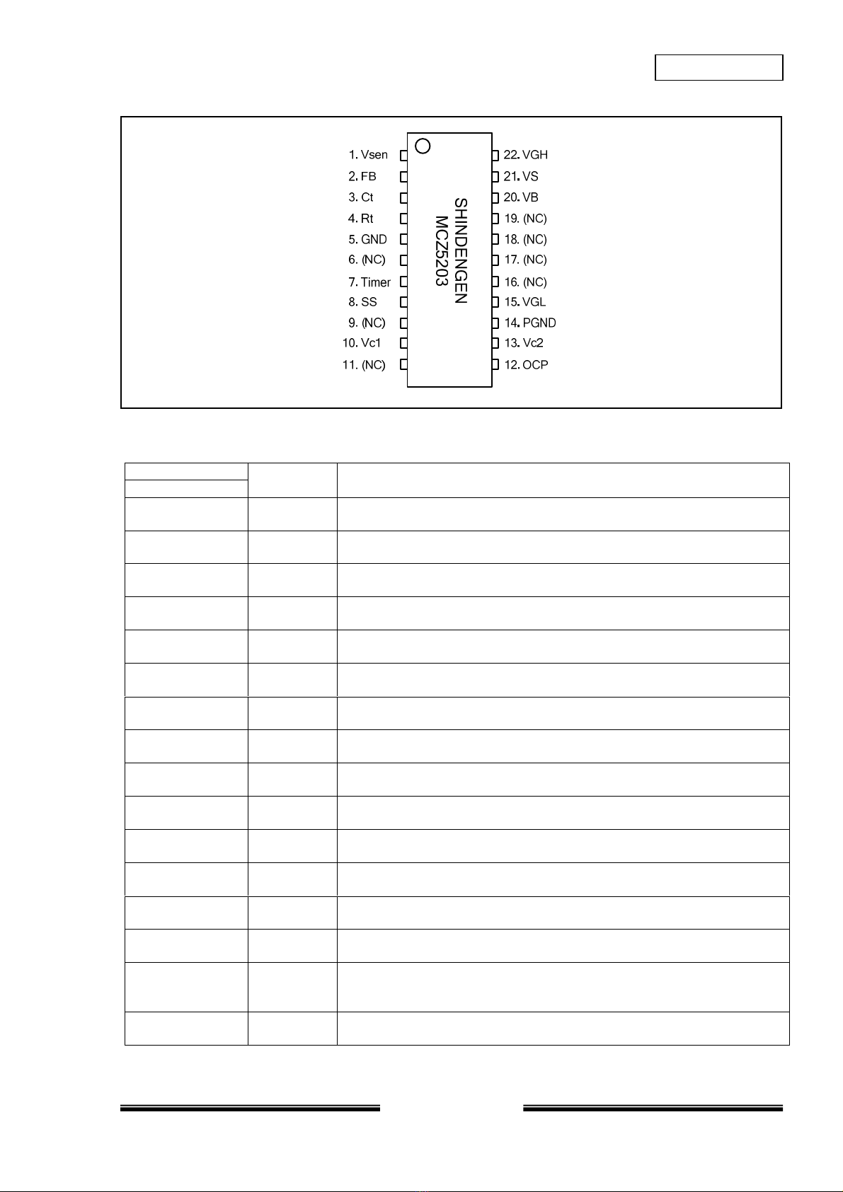
1.3 Pin assignment
1.4 Functions
Pin number
SOP22 name function
1 Vsen DC input voltage monitoring
2 FB Feedback signal input with Feedback loop open detection
3 Ct Timing capacitor Ct determines Dead time and fmin (minimum
operating frequency) and also fss(startup frequency)
4 Rt Timing resistor Rt determines fmin
5 GND Signal ground.
This pin should be connected to PGND directly.
7 TIMER CTimer determines the time period of burst mode in OCP or another
abnormal operation.
8 SS Startup timing capacitor Css determines the soft-starting time
10 Vc1 Voltage supply input for control circuit with 13.5V/8.4V UVLO
Maximum rated voltage is 35V
12 OCP Main resonant current sensing with +0.345V threshold for peak
current limiting ,+/- 60mV for didt protection
13 Vc2 Voltage regulator output for Gate driver
Vc2=10V.
14 PGND Power ground
This pin should be connected to low side MOSFET source directly
15 VGL Low side gate driveroutput
6,9,11,16,
17,18,19 (NC) No connection
20 VB Voltage source of High side gate driver supplied from Vc2 through
bootstrap circuit
21 VS Floating driver reference voltage ( = Source pin of high side
MOSFET)
22 VGH High side gate driveroutput
Table of contents


