SIFANG CSC-196 User manual

CSC-196 Time Synchronization Device
for Power System
Manual

CSC-196 Time synchronization device for
power system
Manual
Compiled: Wu Yalu
Checked: Hu Jiong
Standardized: Liang Luhui
Inspected: Zhu Qichen
Publication No.: V1.00
File No. : 0SF.459.057(E)
Date of issuing: August 2010
All rights reserved: Beijing Sifang Automation Co., Ltd.
Note: we keep the right to modification. In case of deviation between the product and the
instruction, please contact us in time, we will provide relative services.
Technical support Tel: 86-10-62986668 Fax: 86-10-62981900

Importance
You are appreciated for use our product. For safe, correct and effective
application of this device, please pay attention to the followings:
1) The instruction is only for CSC-196 (Time synchronization device
for power system).
2) Please read the instruction carefully, and adjust, test and operate
your device accordingly. The documents attached the device (if
any) is preferential.
3) No live plug and touching chips and elements on the printed
circuit board are allowable.
4) Test and inspect this device with qualified instrumentation only.
5) In case of troubles, please contact us in time through the hot line.

Contents
1.General…………………………………………………………………1
1.1.Brief introduction of the device………………………………………………………………...1
1.2.Functions…………………………………………………………………………………….….1
2.Technical parameters…………………………………………………...3
2.1.Main technical parameters……………………………………………………………………...3
2.2.Environmental condition……………………………………………………………….……….6
2.3.Electrical insulation…………………………………………………………………….……….6
2.3.1.Dielectric strength....................................................................................................................6
2.3.2.Insulation resistance.................................................................................................................6
2.4.Mechanical properties…………………………………………………………………………..6
2.4.1.Vibration………………………………………………………………………………………6
2.4.2.Impact…………………………………………………………………………………………6
2.4.3.Bump………………………………………………………………………………………….7
2.5.Electromagnetic compatibility………………………………………………………………….7
2.5.1.Electrostatic discharge immunity.............................................................................................7
2.5.2.Radiated radio-frequency electromagnetic field immunity......................................................7
2.5.3.Electrical fast transient/burst immunity ...................................................................................7
2.5.4.Surge immunity........................................................................................................................7
2.5.5.Power frequency magnetic field immunity..............................................................................7
2.5.6.Pulse magnetic field immunity.................................................................................................7
2.5.7.Damped oscillatory magnetic field immunity..........................................................................7
2.5.8.Oscillatory waves immunity ....................................................................................................7
2.6.Safety performance……………………………………………………………………………..8
2.7.Alarm output contact capacity………………………………………………………………….8
3.1 Cards arrangement……………………………………………………………………………...9
3.2Power supply card (Code D)…………………………………………………………………….9
3.3Main signal receiving card (Code J)…………………………………………………………...10
3.4Sub-signal receiving card (Code JF)…………………………………………………….……..12
3.5Serial port message output card (Code T)……………………………………………….……..13
3.6Idle contact type signal output card (code K)………………………………………………….14
3.7Multimode optical fiber output card (Code F)…………………………………………………15
3.8Differential signal output card (Code C)………………………………………………….……16
3.9TTL output card (Code L)……………………………………………………………………...17
3.10.Network time comparing card (Code N)……………………………………………….…….18

3.11.IRIG-B (AC) output card (Code A)………………………………………………………….19
3.12.Monomode optical fiber output card (Code H)……………………………………………...20
3.13.Front panel………………………………………………...…………………………………20
4.Engineering application……………………………………………….25
4.1.About the typical time synchronization systems………………………………………………25
4.1.1.Basic time synchronization system ........................................................................................25
4.1.2.Master-slave mode time synchronization system...................................................................25
4.1.3.Run-standby mode time synchronization time transmission system......................................26
4.2.CSC-196 Configuration scheme………………………………………………………………27
4.2.1.General description of the configuration scheme...................................................................27
4.2.2.Software configuration of the input channel..........................................................................27
4.2.3.Master-slave mode time synchronization system(single channel GPS)............................28
4.2.4.Master-slave mode time synchronization system (GPS standby each other).........................29
4.2.5.Master-slave mode time synchronization system(GPS/BD standby other each)..............31
4.2.6.Run-standby mode time synchronization system (GPS standby each)............................32
4.2.7.Connecting to time synchronization network.........................................................................35
4.2.8.Connecting method of client-side equipments.......................................................................36
5.Installation, commissioning and operating maintenance at site………37
5.1.Requirement for antenna installation………………………………………………………….37
5.1.1.GPS antenna installation requirement....................................................................................37
5.1.2.Requirement for BD antenna installation...............................................................................38
5.2.Routine initialization…………………………………………………………………………..38
5.3.Initialization of BD signal receiving card……………………………………………………..39
5.4.Operating maintenance………………………………………………………………………..40
6.Ordering information………………………………………………….45
6.1.Requirement for ordering……………………………………………………………………...45
6.2.Configuration list of single device…………………………………………………………….46
6.3.Available information code for the device…………………………………………………….50
Appendix A Operating instruction of configuration serial port……….51
A.1 Connection of configuration serial port………………………………………………………51
A.2 Definition of configuration serial port wire…………………………………………………..52
A.3 CSC-196 device default configuration………………………………………………………..52
A.4 Serial port configuration order………………………………………………………………..53
A.5 Operating state definition and fault handling method………………………………………...67

Appendix B Configuration parameters displayed on the front panel…70
Appendix C Configuration method of network time comparing card...71
Appendix D Serial port message output format………………………74
Appendix E IRIG-B Standard format…………………………………77
Appendix F Operating mode of the run-standby mode time
synchronization system………………………………………………....80

CSC-196 Time synchronization device for power system Manual
1
1. General
1.1. Brief introduction of the device
The CSC-196 power system synchronous clock device (hereinafter as “the device” for short) is a
timing reference signal output device that is developed and produced by Beijing Sifang
Automation Co., Ltd. (hereinafter as “Sifang” for short) according to Specifications of time
synchronization system for power system for supplying accurate time synchronous signals to
equipments at substations and dispatching ends such as the PMU, protection, monitor, fault
oscillograph and so on.
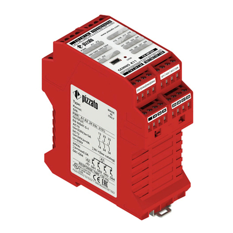
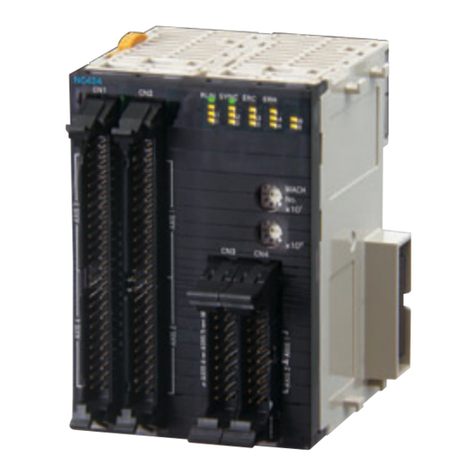
Fig. 1-1 Picture of CSC-196
1.2. Functions
1) It is designed according Specifications of time synchronization system for power system
strictly. Multi-type time synchronization systems such as the basic mode, master slave mode
and run-standby mode, the working logic and technical parameters of the clock comply with
the specifications, in addition, output signals can be expended freely.
2) Multi external time reference signals such as GPS, Beidou and IRIG-B (DC), up to 4 time
reference signals are available per clock, the signals are mutual redundant hot standby, with
excellent reliability.
3) The core time-transfer algorithm of the device is based on the patent 200410009685.2
(“Beidou No.1”navigation satellite system and GPS mutual standby time transfer method and
device), which may filtrate random error of input signal second punctual edge, when multi
input time signal is accessed, it can identify and follow the best input signal automatically and

CSC-196 Time synchronization device for power system Manual
2
guarantee time accuracy of the output signal to be better than 1us, meet requirement of PMU
and so on to accurate time-transfer signals.
4) Many time synchronization signals such as the time comparing pulse, IRIG-B, serial port time
message and network time message (SNTP) can be able to output.
5) Many time synchronization signal interfaces such as optical fiber, idle contact, TTL,
RS-422/485, RS-232 and Ethernet are available.
6) The 19”2U standard rack-type case is adopted, which has modularization design, input
signal receiving cards and time signal output cards can be configured as required.
7) Both the master clock and slave clock have built-in accurate crystal oscillators, which may
keep time synchronization signal output automatically even in case of external time reference
signal trouble, time accuracy under self time keeping state is better than 0.92us/min (55us /h).
8) It supports the time compensation function, can set compensating parameters of all input
signals and output signals freely to compensate error caused by long distance signal
transmission, thereby guarantee output signal accuracy of each master clock or slave clock to
reach ±1us.
9) It supports double power supply hot standby, all output interfaces are buffered outputs.
10) It has good maintainability, its front panel can display working status of the unit, the serial
port can provide detailed operating state information and failure diagnosis information for all
inputs and outputs for finding fault quickly; the input and output time reference signals can be
transferred to the test port to output outside.
11) Treatment of leap second identification complies with Specifications of time synchronization
system for power system and IEEE C37.118-2005, information about leap second can be
obtained in advance, and its forenotice marking is set to meet requirement of PMU.

CSC-196 Time synchronization device for power system Manual
3
2. Technical parameters
2.1. Main technical parameters
1) Rated power voltage: DC 110V, DC 125V or DC 220V.
2) Power consumption of power supply: less than 50W.
3) Receiver and antenna
a) Receiver
12 parallel channels, following 12 satellites at the same time;
Receiving sensitivity: Capture < -160 dBW, tracing < -163 dBW;
Capture time: Warm start < 50s;
Cold start < 100s;
Time accuracy: < 500ns
b) Antenna
Sensitivity: ≤-163 dBW
Operating temperature range: - 40℃to +70 ℃
4) Clock configuration plan:
CSC-196 may form all time synchronization systems such as the basic mode, master-slave mode
and run-standby mode by using various signal receiving cards freely, refer to Section 4.2 of this
instruction for details.
Refer to the following table for the Max. input configuration of each device (some Max.
configuration plans are used at site seldom):
Type of input
signal
Max. input configuration (code of signal
receiving card J, JF)
(The device supports any of the following
configuration plans)
Max. antenna
length
(without
repeater)
Signal interface
GPS
1
/
2
1
/
150 m
BNC antenna terminal
BD
/
1
/
1
/
100 m
TNC antenna terminal
IRIG-B
2
2
/
/
4
/
Optical fiber
5) Time comparing pulse output
Pulse type: 1PPS, 1PPM, and 1PPH(1PPM and 1PPH use the common output port, a
device can only output one), programmable pulse (1PPS, 1PPM and 1PPH are available
as required).
Interface type:
a) Idle contact: time accuracy is better than 3us, contact closed is for high level of the
TTL level, contact opened is for the low level of TTL level, jump of the contact

CSC-196 Time synchronization device for power system Manual
4
from close to open is for punctual edge;
b) 820 nm multimode ST fiber interface: time accuracy is better than 1us.
c) 1310 nm monomode SC fiber interface: time accuracy is better than 1us.
d) Differential interface: RS422/RS485 interface, time accuracy is better than 1us.
Pulse width: 105ms.
6) Serial port time message output
Message format: support the standard format of Specifications of time synchronization of
power system and Sifang’s format (Appendix D).
Message output time: output per entire second, entire minute and entire hour are
available.
Output baud rate: 1200, 2400, 4800, 9600 and 19200 bit/s are available.
Interface type: RS-232, RS-422/485, 820 nm multimode ST fiber interface, 1310 nm
monomode SC fiber interface.
The message frame header aligns the second pulse (1PPS) edge, with deviation less than
1ms.
7) IRIG-B output
IRIG-B(DC)
Type of time comparing code: IRIG-B(DC).
Reference standard: Specifications of time synchronization of power system, be
compatible with IEEE C37.118-2005 (Appendix E).
Type of interface: RS-422/485, TTL, 820 nm multimode ST fiber interface and 1310 nm
monomode SC fiber interface.
Time accuracy: better than 1us.
IRIG-B(AC)
Type of time comparing code: IRIG-B(AC)。
Carrier frequency: 1 kHz;
Frequency jitter: ≤1% of carrier frequency;
Signal amplitude(peak to peak value): the high amplitude is 3 V~12 V adjustable,
the typical value is 10V; the low amplitude meets requirement of modulation ratio 3 : 1~
6 : 1, the typical 3 : 1~6 : 1modulation ratio is 3:1;
Output impedance: 600 Ω, transformer buffered output;
Time accuracy of second punctual point: better than 20 μs;
Reference standard: Specifications of time synchronization of power system, be
compatible with IEEE C37.118-2005 (Appendix E).
8) SNTP network time comparing interface output
Type of interface: 10/100 M Ethernet RJ45 interface, physical isolation among different
net port.

CSC-196 Time synchronization device for power system Manual
5
Accuracy of time synchronization: better than 10ms.
9) Configuring method of output card:
Various configuring method based on signal receiving card and power supply card (refer to
Section 3.1), up to 6~8 time signal output cards per device are available, Max. output signal
channels per card:
a) AC B code output card A1:3 channel (if AC B code output is required, there must be
only one A1 per device), A2:8 channels;
b) Multi-mode optical fiber output card: 4;
c) Single-mode optical fiber output card: 2;
d) Network time comparing card: 2.
e) The others are all 8 channels, such as idle contact signal output, serial port message
output, differential signal output, TTLsignal output and so on.
10) Coincidence relation between optical signal and electrical signal:
On of optical fiber refers to high level of the electrical signal, off of optical fiber refers to low
level of the electrical signal.
11) Effective transmission distance of signal
a) Multimode optical fiber interface: <2km;
b) RS232: <15 m;
c) RS422/485: <150 m;
d) Idle contact: <150 m;
e) Ethernet RJ45 electrical interface: <100 m;
f) TTL: <10m(not recommended for strong EMI environment).
g) AC B Code: <1 km;
h) Monomode optical fibe interface: <20 km
12) Structural dimension: Standard 19”2U rack, rear plug mode, LxWxH =
432mm×294mm×88mm.
Hereinafter is the opening for installation:
Fig. 2-1 Opening dimension of CSC-196

CSC-196 Time synchronization device for power system Manual
6
2.2. Environmental condition
The device can operate continuously and normally:
1) Ambient temperature: operating ambient temperature is -10℃~+55℃. Temperature
storage during transportation is -25℃~+70℃. No energizing quantity is applied under
the limiting value, the device has no irreversible change, after temperature resumed, the
device can operate normally.
2) RH: 5%~95%(No condensation and icing inside the device).
3) Atmospheric pressure: 66 kPa~108 kPa.
4) There should be no risks of fire, explosion, corrosion and others, no vibration, impact
and collision beyond description in the instruction.
2.3. Electrical insulation
2.3.1. Dielectric strength
The device can resist the dielectric strength test with AC voltage 2kV (electric circuit) or 500V
(electronic circuit), 50Hz, 1min duration, no striking and flashover according to GB/T
14598.3-1993(eqv IEC60255-5).
2.3.2. Insulation resistance
Measure insulation resistance of the device with an instrument with open circuit voltage 500V, it
should not be less than 100MΩ, comply with IEC60255-5: 2000.
2.4. Mechanical properties
2.4.1. Vibration
Vibratory response: The device can resist Grade 1 vibratory response test specified in GB/T
11287-2000, 3.2.1.
Vibratory durability: The device can resist Grade 1 vibratory durability test specified in GB/T
11287-2000, 3.2.2.
2.4.2. Impact
Impact response test: the device can resist an impact response test with Class 1, GB/T14573-1993,
4.2.1.
Impact durability: the device can resist an impact durability test with Class 1, GB/T14573-1993,

CSC-196 Time synchronization device for power system Manual
7
4.2.2.
2.4.3. Bump
The device can resist a Class 1 bump test specified in GB/T14573-1993, 4.3.
2.5. Electromagnetic compatibility
2.5.1. Electrostatic discharge immunity
The device can resist a Class IV electrostatic discharge immunity test specified in GB/T
17626.2-1998.
2.5.2. Radiated radio-frequency electromagnetic field immunity
The device can resist a Class IV radiated radio –frequency electromagnetic field immunity test
specified in GB/T 17626.3-1998.
2.5.3. Electrical fast transient/burst immunity
The device can resist a Class IV electrical fast transient/burst immunity test specified in GB/T
17626.4-1998.
2.5.4. Surge immunity
The device can resist a Class IV surge immunity test specified in GB/T 17626.5-1998.
2.5.5. Power frequency magnetic field immunity
The device can resist a Class IV power frequency magnetic field immunity test specified in GB/T
17626.8-1998.
2.5.6. Pulse magnetic field immunity
The device can resist a Class IV pulse magnetic field immunity test specified in GB/T
17626.9-1998.
2.5.7. Damped oscillatory magnetic field immunity
The device can resist a Class IV damped oscillatory magnetic field immunity test specified in
GB/T 17626.10-1998.
2.5.8. Oscillatory waves immunity
The device can resist a Class IV oscillatory waves immunity test specified in GB/T

CSC-196 Time synchronization device for power system Manual
8
17626.12-1998.
2.6. Safety performance
The device can comply with safety class I of GB 16836, not less than IP 20.
2.7. Alarm output contact capacity
Operating capacity: if voltage is not more than 250V, allowable long term operating current is 3A,
allowable transient impulse capacity is 62.5VA/30W. Breaking capacity: AC250V(DC30V)/3A.

CSC-196 Time synchronization device for power system Manual
9
3. Hardware description
3.1 Cards arrangement
Hereinafter is the cards installation drawing (the rear view of the case), assembly of cards should
comply with following basic principles:
1) The main signal receiving card is necessary, which must be assembled at position 1 (the
leftmost slot);
2) The main power supply card is necessary, which must be assembled at position 10 (the
rightmost slot);
3) The other cards are optional, where the sub-signal receiving card can adopt one only and must
be assembled at position 2; the standby power supply card can adopt one only and must be
assembled at position 9; the other cards can be assembled freely at position 2 ~ position 9
with free quantity.
Main
signal
receiving
(necessary
)
Sub-
signal
receiving
(optional)
Standby
power
supply
(optional)
Card such as K、T、F、C、N, etc.
Main power
supply
(necessary)
10Position 1 4 5 6 7 8 92 3
Rear view
Fig. 3-1 Arrangement of CSC-196 cards
3.2 Power supply card (Code D)
失电告警
IN-
IN+
1
2失电告警
IN-
IN+
1
2
电源 DC 220V
失电告警
IN-
IN+
1
2
DC
Failure
IN-
IN+
1
2
POWER DC 110V
D
失电告警
IN-
IN+
1
2
DC
Failure
IN-
IN+
1
2
POWER DC 220V
D
失电告警
IN-
IN+
1
2
DC
Failure
IN-
IN+
1
2
POWER DC 125V
D
D1 D2 D3

CSC-196 Time synchronization device for power system Manual
10
Fig. Panel of power supply card
1) There are 3 kinds of optional cards, D1 is a DC 110V card, D2 is a DC 220V card, D3 is a DC
125V card,.
2) Hardwares of the main power supply card and the standby power supply card are same, only
the assembled positions are different.
3) Terminal definition:
a) DC Failure: not normally closed contact;
b) IN- and IN+: power input, the positive and the negative pole are not limited during
connection;
c) 〨: connect the casing, to shielding earth.
3.3 Main signal receiving card (Code J)
GPS Unit
ANT
J1
Config Serial
P+
P-
A1
A2
FiberInputUnit
J2
ConfigSerial
P+
P-
A1
A2
Input1
Input2
Sigle-Mode
FiberInputUnit
J5
ConfigSerial
P+
P-
A1
A2
Input
R
GPS Unit
ANT
J6
Config Serial
P+
P-
A1
A2
Fiber Input Unit
J7
Config Serial
P+
P-
A1
A2
Input1
Input2
Sigle-Mode
Fiber Input Unit
J8
Config Serial
P+
P-
A1
A2
Input
R
Fig. 3-3 Panel of main signal receiving card J
Three optional cards are available:
J1 and J6 are GPS signal receiving cards, the antenna connects ANT, with interface of BNC.
J2 is the multimode optical fiber signal receiving card, the interface is 820nm multimode ST

CSC-196 Time synchronization device for power system Manual
11
optical fiber interface, Max. 2 channels of time reference signals can be connected to each card,
the input signals have two kinds:
a) IRIG-B(DC) time comparing code: the first channel of IRIG-B time comparing codes
connect to Input 1, the second channel of IRIG-B time comparing codes connect to
Input 2, 2 channels of input time reference signals are available for each receiving
card.
b) PPS+ time message: the PPS optical fiber connects to Input 1, the time message
optical fiber connects to Input 2, since PPS and time message form one channel of
time signals, only one channel of time reference signals is supported by each receiving
card.
J5 is the single-mode optical fiber receiving card with the 1310nm monomode SC optical fiber
interface, only 1 channel time reference signals is available for each receiving card.
There are input indicators on J2 and J5 to show input signal status directly.
There are accurate crystal oscillators inside J1, J2 and J5. Furthermore, high quality imported
constant temperature crystal oscillator in J6, J7 and J8 can meet requirement of high punctual
accuracy.
P+ and P- are testing pulse output, TTL interfaces, by setting jumper on the signal receiving card,
signals of input PPS, input IRIG-B, output PPS, PPM, PPH and output IRIG-B can be transferred
to the testing terminal output.
A1 A2 are alarm output contacts, normally open but not keeping type, which will close when the
device is in trouble, and open automatically when trouble is removed, it can act with the panel
Alarm indicator at the same time to drive the external 110V/220V electric contacts.
Config Serial is the serial for configuration information input and return, the interface is the USB
terminal (Note it is a serial actually, never connect other USB devices), which may connect a
computer with supplied debugging line, to use the setting serial to set operating parameters of the
device, or check status of the input signal and output signal of the device. Refer to Appendix A
for details.
Jumper setting of main signal receiving card J:
Jumper
name
Default setting
Remark
J2、J3
Jump to DSP side
J4~J7
J7 jumps to PPS
side, the other
Only two pins of J4~J7 are connected, or signal short circuit is caused.
J4 jumps to GPS/B/F_PPS: transfer the first channel impulse signals on the

CSC-196 Time synchronization device for power system Manual
12
jumpers are open
motherboard to the P+ P- terminals output
J4 jumps to BAK_PPS: transfer the first channel impulses signals on the
sub-board to the P+ P- terminals output
J5 jumps to GPS/B/F_RXD: transfer the second channel impulse signals on
the motherboard to the P+ P- terminals output
J5 jumps to BAK_RXD: transfer the second channel impulses signals on the
sub-board to the P+ P- terminals output
J6 jumps to IRIG-B: transfer output IRIG-B(DC) codes to P+ P- terminals
output
J6 jumps to RES_OUT: reserved, no signal output
J7 jumps to PPS: transfer output to P+ P- terminals output
J7 jumps to PPM: transfer output PPM or PPH to P+ P- terminals output
J8、J9
Jump to the right
side of the card
J15
Switch on
Switch on: use saved configuration in FLASH, configuration parameters of
the device can be modified by the configuration serial;
Disconnection: locking is default.
J16
Disconnection
J17
Disconnection
Switch on: the device enters into the testing mode, output time comparing
signals directly, but error may exist for the reference time, the time quality
nixie tube will switching display between “E”and “4”, this function is only
for testing, disconnect the jumper J17 after testing.
Disconnection: the device enters into the normal operating mode.
3.4 Sub-signal receiving card (Code JF)
GPS Unit
ANT
JF1
Input 1
Input 2
Fiber Input Unit
JF2
BD Unit
JF4
Sigle-Mode
Fiber Input Unit
JF5
Input
R
Fig. 3-4 Panel of sub-signal receiving card JF
There are four kinds of optional cards:
JF1 is the GPS signal receiving card, the antenna connects to ANT, with the interface BNC.
JF2 is the optical fiber signal receiving card, its input signal interface is same with J2.
JF4 is the BD signal receiving card, with the antenna interface of TNC(with thread).
JF5 is the single-mode optical fiber receiving card, its input signal interface is same with J5.

CSC-196 Time synchronization device for power system Manual
13
Jumper setting of the sub-signal signal receiving card JF:
Card code
Jumper name
Jumper setting method
JF1
J2, J3
Jump to the side of
GPS/B/F
J8, J9
Jump to the right side
of the card
JF2, JF5
J2, J3
Jump to the side of
GPS/B/F
JF4
J2
Jump to the right side
of the card
3.5 Serial port message output card (Code T)
失电
IN-
1-
1+
2-
2+
3-
3+
4-
4+
5-
5+
6-
6+
7-
7+
8-
8+
Serial Unit
T
Fig. 3-9 Panel of serial port message output card T1/T2
1) There are two types of serial port message output cards with codes of T1 and T2, the mark on
the card plate is T, 8 channels of serial port time comparing message output are available for
each card. Distinguishing T1 and T2: there is card drawing number on the label inside the
card, 6SF.007.119.1 refers to T1, and 6SF.007.119.2 refers to T2.
2) Jumper setting:
Code of
card
Output interface
Jumper
name
Jumper setting
method
T1
Channel 1~8 for RS-232 output
J3
All jump to the
side of 232
T2
Channel 1~4 for RS-232 output, and channel 5~8
for RS-422 output
J3
All jump to the
side of 422
Jumper
name
Jumper setting method
Remark
J2
RPM
8 channels of outputs are all RPM message
RPS(Default setting)
8 channels of outputs are all RPS message

CSC-196 Time synchronization device for power system Manual
14
Type, baud rate and output interval of the RPS and RPM message can be set through the
configuration serial port, refer to Appendix A. Default setting is Sifang second message from
RPS, and Sifang minute message from RPM.
3) Terminal definition:
When the output interface is RS-232, the output terminal “+”is TXD, “-“is GND; definition of
common PC 9-pin serial port: 2-RXD, 5-GND; so connect the output terminal “+”to the second
pin of the PC serial port, and “-“to the fifth pin.
When the output interface is RS-422, the output terminals “+”and “-“correspond to the positive
and negative poles of the differential signal respectively.
3.6 Idle contact type signal output card (code K)
失电
IN-
1-
1+
2-
2+
3-
3+
4-
4+
5-
5+
6-
6+
7-
7+
8-
8+
Dry Contact Unit
K
Fig. 3-7 Panel of pulse output card K
1) The card code is K, the card baffle printing is K, support 8 channels of idle contact type time
comparing pulse output, each channel output can be set as second pulse, minute pulse (hour
pulse), IRIG-B(DC), and programmable pulse output. Card K is upgrading version of
Card P, which is recommended.
2) Jumper setting method: printing on J1 jumper is “CH1~CH8”, corresponding to 8 outputs
respectively. Pay attention to one channel can choose only one kind of signal output.
Jumper
name
Jumper setting method
Remark
J1
PPS(Default setting)
Output second pulse 1PPS
PPM
Default output minute pulse 1PPM,output hour pulse
1PPH is also available by configuration serial port
setting
IRIG-B
Output IRIG-B(DC)
Table of contents
