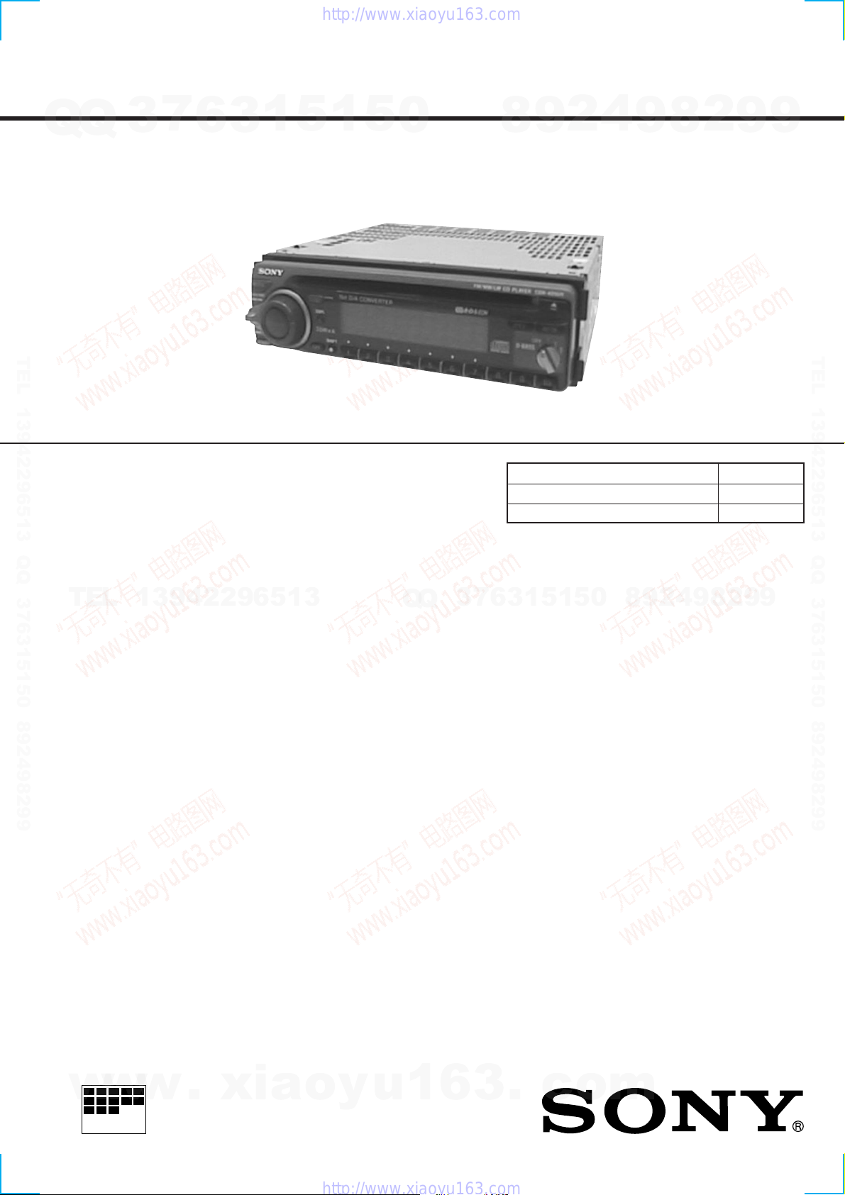
Sony CDX-4260R User manual

1
MICROFILM
Model Name Using Similar Mechanism CDX-4180R
CD Drive Mechanism Type MG-363X-121
Optical Pick-up Name KSS-521A
SERVICE MANUAL
AEP Model
UK Model
CDX-4260R
FM/MW/LW COMPACT DISC PLAYER
CD player section
System Compact disc digital audio
system
Signal-to-noise ratio 90 dB
Frequency response 10 – 20,000 Hz
Wow and flutter Below measurable limit
Tuner section
FM
Tuning range 87.5 – 108.0 MHz
Aerial terminal External aerial connector
Intermediate frequency 10.7 MHz
Usable sensitivity 12 dBf
Selectivity 75 dB at 400 kHz
Signal-to-noise ratio 65 dB (stereo),
68 dB (mono)
Harmonic distortion at 1 kHz
0.8% (stereo),
0.6% (mono)
Separation 35 dB at 1 kHz
Frequency response 30 – 15,000 Hz
MW/LW
Tuning range MW: 531 – 1,602 kHz
LW: 153 – 281 kHz
Aerial terminal External aerial connector
Intermediate frequency 10.7 MHz / 450 kHz
Sensitivity MW: 30 µV
LW: 50 µV
SPECIFICATIONS
Power amplifier section
Outputs Speaker outputs
(sure seal connectors)
Speaker impedance 4 – 8 ohms
Maximum power output 40 W ×4 (at 4 ohms)
General
Outputs Line output (1)
Power aerial relay control
lead
Power amplifier control
lead
Tone controls Bass ±8 dB at 100 Hz
Treble ±8 dB at 10 kHz
Power requirements 12 V DC car battery
(negative ground)
Dimensions Approx. 178 ×50 ×185 mm
(w/h/d)
Mounting dimension Approx. 182 ×53 ×162 mm
(w/h/d)
Mass Approx. 1.2 kg
Supplied accessories Parts for installation and
connections (1 set)
Front panel case (1)
Design and specifications are subject to change without
notice.
w
w
w
.
x
i
a
o
y
u
1
6
3
.
c
o
m
Q
Q
3
7
6
3
1
5
1
5
0
9
9
2
8
9
4
2
9
8
T
E
L
1
3
9
4
2
2
9
6
5
1
3
9
9
2
8
9
4
2
9
8
0
5
1
5
1
3
6
7
3
Q
Q
TEL 13942296513 QQ 376315150 892498299
http://www.xiaoyu163.com

2
Solder bridge
SAFETY-RELATED COMPONENT WARNING!!
COMPONENTS IDENTIFIED BY MARK !OR DOTTED LINE
WITH MARK !ON THE SCHEMATIC DIAGRAMS AND IN
THE PARTS LIST ARE CRITICAL TO SAFE OPERATION.
REPLACE THESE COMPONENTS WITH SONY PARTS WHOSE
PART NUMBERS APPEAR AS SHOWN IN THIS MANUAL OR
IN SUPPLEMENTS PUBLISHED BY SONY.
SERVICE NOTE
CAUTION
Use of controls or adjustments or performance of proce-
dures other than those specified herein may result in haz-
ardous radiation exposure.
Notes on Chip Component Replacement
•Never reuse a disconnected chip component.
•Notice that the minus side of a tantalum capacitor may be dam-
aged by heat.
NOTES ON HANDLING THE OPTICAL PICK-UP BLOCK
OR BASE UNIT
The laser diode in the optical pick-up block may suffer electrostatic
breakdown because of the potential difference generated by the
charged electrostatic load, etc. on clothing and the human body.
During repair, pay attention to electrostatic breakdown and also use
the procedure in the printed matter which is included in the repair
parts.
The flexible board is easily damaged and should be handled with
care.
NOTES ON LASER DIODE EMISSION CHECK
The laser beam on this model is concentrated so as to be focused on
the disc reflective surface by the objective lens in the optical pick-
up block. Therefore, when checking the laser diode emission, ob-
serve from more than 30 cm away from the objective lens.
NOTES ON PICK-UP FLEXIBLE BOARD
The pick-up flexible board in this set is secured to the optical pick-
up with an adhesive tape. Once the tape is removed, an adhering
force becomes weak, and it cannot be reused.
Therefore, if the optical pick-up is replaced, replace also the pick-
up flexible board with a new one.
– main board (side B) –
NOTEFOR REPLACEMENT OF COMPLETE MAIN BOARD
The complete MAIN board (A-3294-762-A) of this set can be set to
address the specification for each destination by shorting or open-
ing one solder bridge of the MAIN board on theAEP and UK mod-
els and German models :
AEP and UK models : short
German model : open
The solder bridge below shold be opened when replacing the com-
plete MAIN board on the German model.
w
w
w
.
x
i
a
o
y
u
1
6
3
.
c
o
m
Q
Q
3
7
6
3
1
5
1
5
0
9
9
2
8
9
4
2
9
8
T
E
L
1
3
9
4
2
2
9
6
5
1
3
9
9
2
8
9
4
2
9
8
0
5
1
5
1
3
6
7
3
Q
Q
TEL 13942296513 QQ 376315150 892498299
http://www.xiaoyu163.com

3
TABLE OF CONTENTS
1. GENERAL
Location of controls.................................................................4
Getting Started......................................................................... 4
Setting the clock ...................................................................... 4
CD Player ................................................................................ 4
Radio ....................................................................................... 5
RDS ......................................................................................... 5
Other Functions ....................................................................... 7
Connections ............................................................................. 8
2. DISASSEMBLY
2-1. Cover ................................................................................. 10
2-2. Front Panel Assy ............................................................... 10
2-3. Sub Panel (1) Assy ............................................................ 11
2-4. CD Mechanism Block .......................................................11
2-5. Main Board ....................................................................... 12
2-6. Heat Sink ........................................................................... 12
2-7. Chassis (T) Sub Assy ........................................................ 13
2-8. Lever Assy ......................................................................... 13
2-9. Servo Board ....................................................................... 14
2-10. Roller Assy ........................................................................ 14
2-11. Chassis (OP) (O/S) Assy ................................................... 15
2-12. Optical Pick-up Block .......................................................15
3. ELECTRICAL ADJUSTMENTS
Tuner Section......................................................................... 16
CD Section ............................................................................ 19
4. DIAGRAMS
4-1. IC Pin Description............................................................. 20
4-2. Block Diagram –CD Section–........................................... 22
4-3. Block Diagram –Tuner Section– ....................................... 23
4-4. Block Diagram –Display Section–.................................... 24
4-5. Circuit Boards Location .................................................... 25
4-6. Printed Wiring Boards –CD Mechanism Section–............26
4-7. Schematic Diagram –CD Mechanism Section– ................ 27
4-8. Printed Wiring Board –Main Section– .............................. 28
4-9. Schematic Diagram –Main Section (1/3)– ........................ 30
4-10. Schematic Diagram –Main Section (2/3)– ........................ 31
4-11. Schematic Diagram –Main Section (3/3)– ........................ 32
4-12. Schematic Diagram –Display Section–............................. 33
4-13. Printed Wiring Board –Display Section– .......................... 34
5. EXPLODED VIEWS
5-1. Chassis Section ................................................................. 39
5-2. Front Panel Section ........................................................... 40
5-3. CD Mechanism Section (1) ............................................... 41
5-4. CD Mechanism Section (2) ............................................... 42
5-5. CD Mechanism Section (3) ............................................... 43
6. ELECTRICAL PARTS LIST ........................................ 44
w
w
w
.
x
i
a
o
y
u
1
6
3
.
c
o
m
Q
Q
3
7
6
3
1
5
1
5
0
9
9
2
8
9
4
2
9
8
T
E
L
1
3
9
4
2
2
9
6
5
1
3
9
9
2
8
9
4
2
9
8
0
5
1
5
1
3
6
7
3
Q
Q
TEL 13942296513 QQ 376315150 892498299
http://www.xiaoyu163.com

10
2
front panel assy
1
Push the button (release).
1
claw
4
cover
2
claw
3
claws
SECTION 2
DISASSEMBLY
Note : Follow the disassembly procedure in the numerical order given.
2-1. COVER
2-2. FRONT PANEL ASSY
w
w
w
.
x
i
a
o
y
u
1
6
3
.
c
o
m
Q
Q
3
7
6
3
1
5
1
5
0
9
9
2
8
9
4
2
9
8
T
E
L
1
3
9
4
2
2
9
6
5
1
3
9
9
2
8
9
4
2
9
8
0
5
1
5
1
3
6
7
3
Q
Q
TEL 13942296513 QQ 376315150 892498299
http://www.xiaoyu163.com

11
7
PTT 2.6x6
3
PTT 2.6x6
6
PTT 2.6x
6
2
PTT 2.6x6
4
CNP700
8
bracket (M/D)
5
CD mechanism block
1
PTT 2.6x6
1
PTT 2.6x6
3
PTT 2.6x6
5
claw
4
claw
6
sub panel (1) assy
2
PTT 2.6x6
2-4. CD MECHANISM BLOCK
2-3. SUB PANEL (1) ASSY
w
w
w
.
x
i
a
o
y
u
1
6
3
.
c
o
m
Q
Q
3
7
6
3
1
5
1
5
0
9
9
2
8
9
4
2
9
8
T
E
L
1
3
9
4
2
2
9
6
5
1
3
9
9
2
8
9
4
2
9
8
0
5
1
5
1
3
6
7
3
Q
Q
TEL 13942296513 QQ 376315150 892498299
http://www.xiaoyu163.com

12
4
ground point screws
(PTT 2.6x6)
5
ground point screw
(PTT 2.6x6)
1
PTT 2.6x8
6
MAIN board
3
PTT 2.6x
8
2
PTT 2.6x8
2
PTT 2.6x12
4
heat sink
1
PTT 2.6x8
3
PTT 2.6x
8
2-5. MAIN BOARD
2-6. HEAT SINK
w
w
w
.
x
i
a
o
y
u
1
6
3
.
c
o
m
Q
Q
3
7
6
3
1
5
1
5
0
9
9
2
8
9
4
2
9
8
T
E
L
1
3
9
4
2
2
9
6
5
1
3
9
9
2
8
9
4
2
9
8
0
5
1
5
1
3
6
7
3
Q
Q
TEL 13942296513 QQ 376315150 892498299
http://www.xiaoyu163.com

13
5
chassis (T) sub assy
3
P 2x3
4
P 2x3
1
Unsolder the
lead wires.
gray
white
black
2
P 2x3
4
claws
2
DISC IN SW board
7
lever (L) assy
3
tension spring (LR)
6
lever (R) assy
5
guide (disc)
1
PS 2x4
2-7. CHASSIS (T) SUB ASSY
2-8. LEVER ASSY
w
w
w
.
x
i
a
o
y
u
1
6
3
.
c
o
m
Q
Q
3
7
6
3
1
5
1
5
0
9
9
2
8
9
4
2
9
8
T
E
L
1
3
9
4
2
2
9
6
5
1
3
9
9
2
8
9
4
2
9
8
0
5
1
5
1
3
6
7
3
Q
Q
TEL 13942296513 QQ 376315150 892498299
http://www.xiaoyu163.com

14
5
PS 2x4
1
CN3
3
P 2x3
4
loading motor assy
7
SERVO board
2
CN2
6
PS 2x4
Fig. 1
4
PS 2x3
5
LOAD SW board
1
tension spring (RA)
2
arm (roller)
3
roller assy
washer arm arm
washer washers
2-9. SERVO BOARD
2-10. ROLLER ASSY
• When installing, take note of the positions
arm (roller) and washers. (Fig. 1)
w
w
w
.
x
i
a
o
y
u
1
6
3
.
c
o
m
Q
Q
3
7
6
3
1
5
1
5
0
9
9
2
8
9
4
2
9
8
T
E
L
1
3
9
4
2
2
9
6
5
1
3
9
9
2
8
9
4
2
9
8
0
5
1
5
1
3
6
7
3
Q
Q
TEL 13942296513 QQ 376315150 892498299
http://www.xiaoyu163.com

15
1
P 2x3
2
sled motor assy
3
optical pick-up block
1
tension spring (KF1)
8
compression spring (FL)
7
chassis (OP) (O/S) assy
9
compression spring (FL)
2
tension spring (KR1)
5
Fit lever (D) in the
direction of the arrow.
3
damper (T)
4
damper (T)
6
Turn loading ring in the
direction of the arrow.
2-11. CHASSIS (OP) (O/S) ASSY
2-12. OPTICAL PICK-UP BLOCK
w
w
w
.
x
i
a
o
y
u
1
6
3
.
c
o
m
Q
Q
3
7
6
3
1
5
1
5
0
9
9
2
8
9
4
2
9
8
T
E
L
1
3
9
4
2
2
9
6
5
1
3
9
9
2
8
9
4
2
9
8
0
5
1
5
1
3
6
7
3
Q
Q
TEL 13942296513 QQ 376315150 892498299
http://www.xiaoyu163.com

16
SHUF
SHUF
SHUF
FM RF signal
generator
0.01
µ
F
antenna
terminal
set
SECTION 3
ELECTRICAL ADJUSTMENTS
Carrier frequency : 98.00 MHz
Output level : 22 dB (12.6 µV)
Mode : mono
Modulation : 1 kHz, 22.5 kHz deviation (30%)
Procedure :
1. Set to the test mode.
2. Push the SOURCE button and set to FM.
Display
FM Auto Scan/Stop Level Adjustment
Setting :
D-BASS switch : OFF
SOURCE button : FM
3. Push the preset 3 button.
Display
TUNER SECTION 0 dB = 1 µV
Cautions during repair
When the tuner unit is defective, replace it by a new one
because its internal block is difficult to repair.
TEST MODE
This set have the test mode function. In the test mode, FM Auto
Scan/Stop Level and MW Auto Scan/Stop Level adjustments can
be performed easier than it in ordinary procedure.
<Set the Test Mode>
1. Set the “OFF” mode.
2. Push the preset 4 button.
3. Push the preset 5 button.
4. Press the preset 1 button for more than two seconds.
5. Then the display indicates all lights, the test mode is set.
<Release the Test Mode>
1. Push the OFF button.
Note on Adjustment
The adjustments of tuner section, should be performed according
to the following sequence.
1. FM Auto Scan/Stop Level Adjustment
2. FM Stereo Separation Adjustment
3. FM RDS S-Meter Adjustment
4. MW Auto Scan/Stop Level Adjustment
4. Adjust with the volume RV2 on TU601 so that the “FM”
indication turns to “FM0” indication on the display window.
But, in case of already indicated “FM0”, turn the RV2 so that
put out light “0” indication and adjustment.
Display
Adjustment Location : See page 18.
w
w
w
.
x
i
a
o
y
u
1
6
3
.
c
o
m
Q
Q
3
7
6
3
1
5
1
5
0
9
9
2
8
9
4
2
9
8
T
E
L
1
3
9
4
2
2
9
6
5
1
3
9
9
2
8
9
4
2
9
8
0
5
1
5
1
3
6
7
3
Q
Q
TEL 13942296513 QQ 376315150 892498299
http://www.xiaoyu163.com

17
SHUF
SHUF
FM RF signal
generator
0.01
µ
F
antenna
terminal
set
+
–
FM RF signal
generator
0.01
µ
F
antenna
terminal
set
LINE OUT REAR
10 k
Ω
level meter
FM Stereo Separation Adjustment
Setting :
D-BASS switch : OFF
SOURCE button: FM
Carrier frequency : 98.00 MHz
Output level : 70 dB (3.2 mV)
Mode : stereo
Modulation : main : 1 kHz, 20 kHz deviation (26.7%)
sub : 1 kHz, 20 kHz deviation (26.7%)
19 kHz pilot : 7.5 kHz deviation (10%)
FM stereo Level meter Level meter
signal generator connection reading (dB)
output channel
L-CH L-CH A
B
R-CH L-CH Adjust RV4 on TU601
for nimum reading.
R-CH R-CH C
D
L-CH R-CH Adjust RV4 on TU601
for minimum reading.
L-CH stereo separation : A– B
R-CH stereo separation : C– D
The separations of both channels should be equal.
Specification : Separation more than 28 dB
Adjustment Location : See page 18.
Procedure :
Carrier frequency : 98.00 MHz
Output level : 35 dB (56.2 µV)
Mode : mono
Modulation : no modulation
Procedure :
1. Set to the test mode. (See page 16.)
2. Push the SOURCE button and set to FM.
Display
FM RDS S-Meter Adjustment
Setting :
D-BASS switch : OFF
SOURCE button : FM
3. Push the preset 10 button.
4. Adjust RV801 so that the display indication is “16.0”.
Display
Specification : Display indication : 15.8 to 16.2
Adjustment Location : See page 18.
w
w
w
.
x
i
a
o
y
u
1
6
3
.
c
o
m
Q
Q
3
7
6
3
1
5
1
5
0
9
9
2
8
9
4
2
9
8
T
E
L
1
3
9
4
2
2
9
6
5
1
3
9
9
2
8
9
4
2
9
8
0
5
1
5
1
3
6
7
3
Q
Q
TEL 13942296513 QQ 376315150 892498299
http://www.xiaoyu163.com

18
TU601
RV1
MW AUTO SCAN/
STOP LEVEL ADJ
RV2
FM AUTO SCAN/
STOP LEVEL ADJ
RV801
FM RDS
S-METER ADJ
RV4
FM STEREO
SEPARATION ADJ
TP
SHUF
TP
SHUF
TP
SHUF
AM RF signal
generator AM dummy
antenna (50
Ω
)
set
antenna
terminal
30
Ω
15 pF
65 pF
MW Auto Scan/Stop Level Adjustment
Setting :
D-BASS switch : OFF
SOURCE nMODE button : MW
Carrier frequency : 999 kHz
30% amplitude
modulation by
1 kHz signal
output level : 33 dB (44.7 µV)
Procedure :
1. Set to the test mode. (See page 16.)
2. Push the SOURCE button.
3. Push the MODE button and set to MW.
Display
4. Push the preset 3 button.
Display
5. Adjust with the volume RV1 on TU601 so that the “MW”
indication turns to “MW0” indication on the display window.
But, in case of already indicated “MW0”, turn the RV1 so that
put out light “0” indication and adjustment.
Display
Adjustment Location : tuner unit (TU601)
w
w
w
.
x
i
a
o
y
u
1
6
3
.
c
o
m
Q
Q
3
7
6
3
1
5
1
5
0
9
9
2
8
9
4
2
9
8
T
E
L
1
3
9
4
2
2
9
6
5
1
3
9
9
2
8
9
4
2
9
8
0
5
1
5
1
3
6
7
3
Q
Q
TEL 13942296513 QQ 376315150 892498299
http://www.xiaoyu163.com

19
IC3
CN1 IC1
CN2
FOCUS GAIN ADJ
RV4
TP
(RF. GND)
IC2
TP
(RF) CN3
RV1
FOCUS BIAS ADJ
RF signal waveform VOLT/DIV: 200 mV
TIME/DIV: 500 nS
level: 1.0 – 1.5 Vp-p
SERVO board
TP (RF)
TP (RF. GND)
oscilloscope
+
–
CD SECTION
Note:
1. CD Block basically constructed to operate without adjustment.
Therefore, check each item in order given.
2. UseYEDS-18 disc (3-702-101-01) unless otherwise indicated.
3. Use the oscilloscope with more than 10 MΩimpedance.
4. Clean an objective lens by an applicator with neutral detergent
when the signal level is low than specified valuewiththefollowing
checks.
Focus Bias Adjustment
Setting: This adjustment is performed with the set placed
horizontally.
Focus Gain Adjustment (Coarse adjustment)
Thisadjustment isnot requiredunlessthe followingparts arereplaced:
• Optical pick-up
•RV4
Procedure:
1. Set RV4 to the standard position. (mechanical center)
2. Check whether operation noise (while noise type) caused by
the 2-axis device (lens section of the optical pick-up) is
abnormally loud.
If the operation noise is too loud, turn RV4 slightly counter-
clockwise.
• If the gain is too low:
Focus does not function and no music is selected.
• If the gain is too high:
Noise caused by scratches and dust is heard and the operation
becomes unstable.
Adjustment Location: servo board
Adjustment Location: servo board (component side)
Procedure:
1. Connect an oscilloscope between TP (RF) and TP (RF. GND)
on the SERVO board.
2. Connect the power supply.
3. Push the RESET button (S900) on the MAIN board.
4. Insert the disc (YEDS-18) and playback.
5. Adjust RV1 so thatthe oscilloscope waveformis clear andcheck
RF signal level is correct or not.
Note: Clear RF signal waveform means that the sharp “≈” can be
clearly distinguished at the center of the waveform.
• When observing the eye pattern, set the oscilloscope toAC range
and raise the vertical sensitivity so that it may be easily seen.
Adjustment Location: servo board
w
w
w
.
x
i
a
o
y
u
1
6
3
.
c
o
m
Q
Q
3
7
6
3
1
5
1
5
0
9
9
2
8
9
4
2
9
8
T
E
L
1
3
9
4
2
2
9
6
5
1
3
9
9
2
8
9
4
2
9
8
0
5
1
5
1
3
6
7
3
Q
Q
TEL 13942296513 QQ 376315150 892498299
http://www.xiaoyu163.com

20
4-1. IC PIN DESCRIPTION
• IC801 MB90574APMT-G-212-BND (SYSTEM CONTROL)
Pin No. Pin Name I/O Pin Description
1 LD ON O Laser ON/OFF control output
2 FOK I Focus OK signal detection input
3 XLAT25 O CD signal processing latch output
4 DATA25 O CD signal serial data output
5 XRST O Reset output to CD signal processor IC.
6 GFS I GFS signal detection input
7 NIL — Not used. (Connect to ground in this set.)
8 VCC — Power supply pin (+5 V)
9 – 11 NIL — Not used. (Open)
12 FLS SI/NOSE1 I Front panel attachment detection input
13 LCD SO/FLS SO O LCD serial data output
14 LCD CKO O LCD serial clock output
15 BEEP O BEEP output
16 NIL — Not used. (Open)
17 SQ SI I Sub Q data input
18 NIL — Not used. (Connect to ground in this set.)
19 SQ CKO O Sub Q read clock output
20 UNI SI I SONY BUS system serial interface input
21 UNI SO O SONY BUS system serial interface output
22 UNI CK I/O SONY BUS system serial clock input/output
23 C IN I Track jump No. count input
24 SIRCS I Remote commander input
25 TXT SI I CD-TEXT data input (Not used in this set.)
26 NIL — Not used. (Connect to ground in this set.)
27 TXT CKO O CD-TEXT data read clock output (Not used in this set.)
28 CLOK25 O CD signal processing serial clock output
29 SYSRST O System reset output
30 DEEMPH O De-emphasis output
31 AMP ATT O Power amplifier attenuator control output
32 MD ON O CD mechanism power control output
33 VSS — Ground
34 C — Power stabilization capacitor pin
35 CD ON O CD power control output
36 BUS ON O BUS ON control output (Not used in this set.)
37 NIL O Power control output of A/D conversion.
38 DVCC — VREF input of D/A converter.
39 DVSS — Ground of D/A converter.
40 NIL — Not used. (Open)
41 ANGLE O LCD view angle alignment output (Not used in this set.)
42 AVCC — Analog power supply pin (+5V)
43 AVRH — VREF + input of A/D converter.
44 AVRL — VREF – input of A/D converter.
45 AVSS — Analog ground
46 – 48 KEY IN0 – 2 I Key input 0 – 2
49 RC IN0 I Rotary commander input 0
50 QUALITY I Noise detection input
51 NIL — Not used. (Connect to ground in this set.)
52 MPDH I Tuner multi path input
53 S-METER I S-meter voltage detection input
54 VCC — Power supply pin (+5 V)
55 NS MASK O Noise detection output
SECTION 4
DIAGRAMS
w
w
w
.
x
i
a
o
y
u
1
6
3
.
c
o
m
Q
Q
3
7
6
3
1
5
1
5
0
9
9
2
8
9
4
2
9
8
T
E
L
1
3
9
4
2
2
9
6
5
1
3
9
9
2
8
9
4
2
9
8
0
5
1
5
1
3
6
7
3
Q
Q
TEL 13942296513 QQ 376315150 892498299
http://www.xiaoyu163.com
Table of contents
Other Sony Car Receiver manuals

Sony
Sony XR-6080 User manual

Sony
Sony CDX-GT55UIW - Fm/am Compact Disc Player User manual

Sony
Sony XR-C6200 User manual

Sony
Sony SDX-3180 User manual

Sony
Sony CDX-GT383 User manual

Sony
Sony XR-C6100 User manual

Sony
Sony XR-530R User manual

Sony
Sony XR-CA640X User manual

Sony
Sony MEX-BT3900U Product guide

Sony
Sony CDX-GT24W - Cd Receiver Mp3/wma Player User manual

Sony
Sony XR-C7300 User manual

Sony
Sony CDX-GT500EE User manual

Sony
Sony DSX-A416BT User manual

Sony
Sony MEX-BT4100P User manual

Sony
Sony CDX-2500R User manual

Sony
Sony RXD-700 User manual

Sony
Sony MEX-BT4100U User manual

Sony
Sony XAV-601BT Product guide

Sony
Sony MEX-GS600BT User manual

Sony
Sony MEX-BT2500 User manual