Sony TC-S9 User manual

SERVICE MANUAL
STEREO CASSETTE DECK
AEP Model
UK Model
E Model
Australian Model
SPECIFICATIONS
TC-S9
Ver 1.0 2001.09
9-873-281-01 Sony Corporation
2001I0500-1 Home Audio Company
C2001.9 ShinagawaTec Service Manual Production Group
TC-S9 is the Tape deck section
in MHC-S9D.
Tape deck Model Name Using Similar Mechanism TC-S3
Section Tape Transport Mechanism Type TCM-230AWR41,
TCM-230MWR41
Dolby noise reduction manufactured under license
from Dolby Laboratories Licensing Corporation.
“DOLBY” and the double-D symbol ;are trade-
marks of Dolby Laboratories Licensing Corporation.
Recording system 4-track 2-channel stereo
Frequency response 60 – 13,000 Hz (±3 dB),
(DOLBY NR OFF) using Sony TYPE I
cassette,
60 – 14,000 Hz (±3 dB),
using Sony TYPE II
cassette
Dimensions (w/h/d)
Approx. 280 x 128 x 330 mm
Mass Approx. 2.4 kg
Design and specifications are subject to change
without notice.

2
TC-S9
TABLE OF CONTENTS
1. SERVICING NOTES ................................................ 3
2. GENERAL
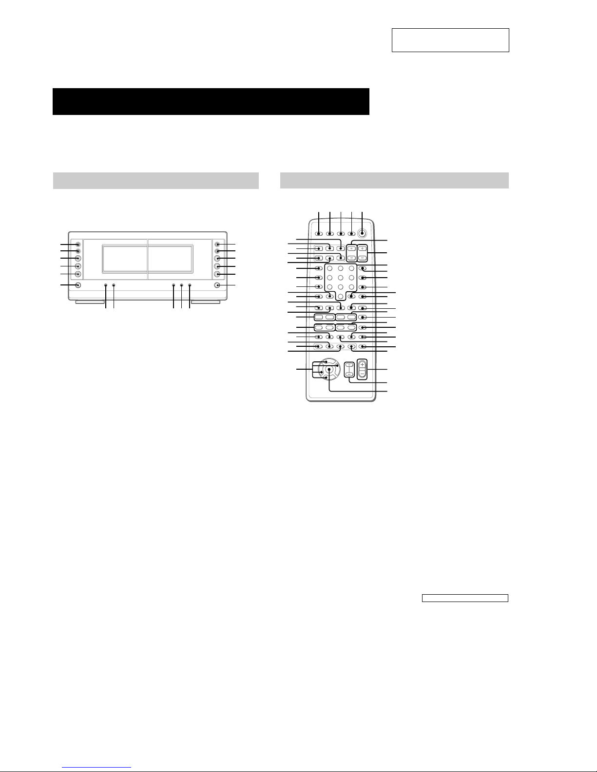
Location of Controls ....................................................... 4
3. DISASSEMBLY
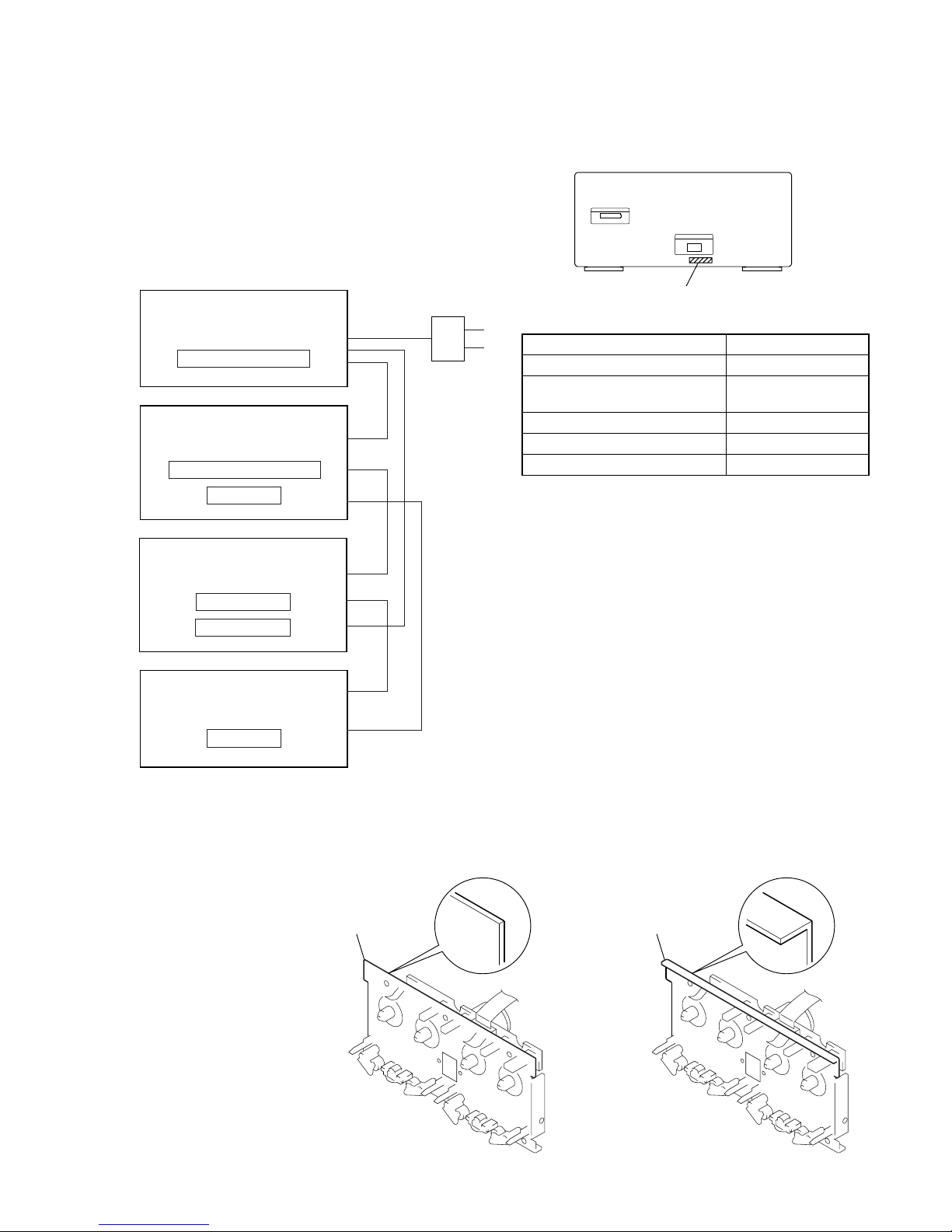
3-1. Disassembly Flow ........................................................... 5
3-2. Case ................................................................................. 5
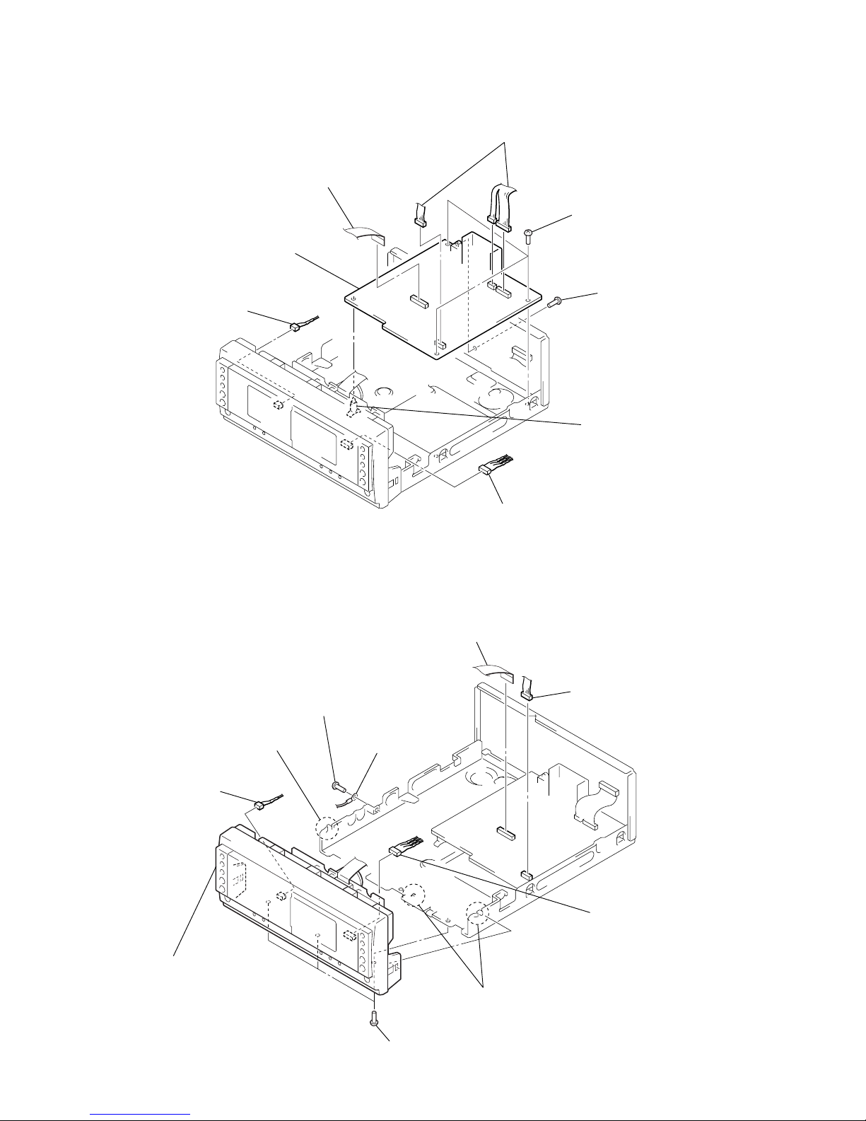
3-3. MAIN Board ................................................................... 6
3-4. Front Panel Section ......................................................... 6
3-5. Tape Mechanism Deck
(TCM-230AWR41, TCM-230MWR41)......................... 7
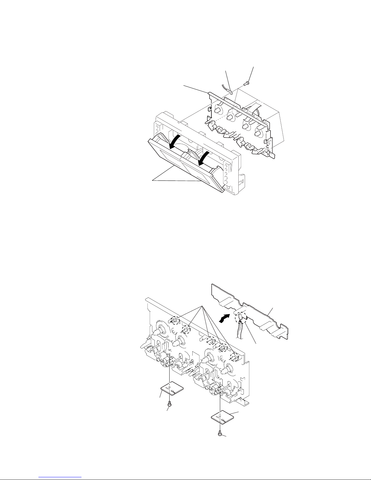
3-6. LEAF SW Board, HEAD (A) Board and
HEAD (B) Board ............................................................ 7
4. TEST MODE.............................................................. 8
5. MECHANICAL ADJUSTMENTS....................... 9
6. ELECTRICAL ADJUSTMENTS......................... 9
7. DIAGRAMS
7-1. Note for Printed Wiring Boards and
Schematic Diagrams ....................................................... 13
7-2. Schematic Diagram –MAIN Section (1/2) –................ 14
7-3. Schematic Diagram –MAIN Section (2/2) –................ 15
7-4. Printed Wirings Boards –MAIN Section –................... 16
7-5. Schematic Diagram –LEAF SW Section –................. 17
7-6. Printed Wiring Board –LEAF SW Section –............... 17
7-7. Schematic Diagram –PANEL Section –....................... 18
7-8. Printed Wiring Boards –PANEL Section –.................. 18
7-9. IC Pin Function Description ........................................... 19
8. EXPLODED VIEWS
8-1. General Section ............................................................... 21
8-2. Front Panel Section ......................................................... 22
8-3. Tape Mechanism Deck Section
(TCM-230AWR41).......................................................... 23
8-4. Tape Mechanism Deck Section
(TCM-230MWR41) ........................................................ 24
8-5. Sub Chassis Assy Section
(TCM-230MWR41) ........................................................ 25
9. ELECTRICAL PARTS LIST ............................... 26
Notes on chip component replacement
•Never reuse a disconnected chip component.
•Notice that the minus side of a tantalum capacitor may be dam-
aged by heat.
SAFETY-RELATED COMPONENT WARNING!!
COMPONENTS IDENTIFIED BY MARK 0OR DOTTED
LINE WITH MARK 0ON THE SCHEMATIC DIAGRAMS
AND IN THE PARTS LIST ARE CRITICAL TO SAFE
OPERATION. REPLACE THESE COMPONENTS WITH
SONY PARTS WHOSE PART NUMBERS APPEAR AS
SHOWN IN THIS MANUAL OR IN SUPPLEMENTS PUB-
LISHED BY SONY.

3
TC-S9
SECTION 1
SERVICING NOTES
Model PART No.
AEP and UK models 4-236-839-0[]
Australian, Saudi Arabia
and Korean models 4-236-839-1[]
E and Singapore models 4-236-839-2[]
Mexican model 4-236-839-3[]
Thai model 4-236-839-4[]
• MODEL IDENTIFICATION
– Rear Panel –
This set is a component of the MHC-S9D.
The MHC-S9D system configuration is as shown below, and there-
fore it does not operate normally unless all four components are
connected.
In performing the repair, connect all components with the system
cables.
Note: The precaution to the users is described on the label stuck
on the back panel (DVD/video CD/CD player) and in the trouble-
shooting section in the Operation Manual.
System Configuration:
POWER SUPPLY
AC IN
TA
MASTER & GRAPHIC µcon
ST
TC µcon
TC
DISPLAY
HTC & MB µcon
DVP
POWER BLOCK
PART No.
• TAPE MECHANISM DECK DISCRIMINATION
TCM-230AWR41 and TCM-230MWR41 are used for the tape
mechanism deck of this set, and they can be discriminated as shown
below.
main chassis
straight L-shape
TCM-230AWR41 TCM-230MWR41
main chassis

4
TC-S9 SECTION 2
GENERAL This section is extracted from
instruction manual.
LOCATION OF CONTROLS
Cassette deck
CD SYNC ta (45, 46)
DIRECTION tf (44, 45, 46, 55)
DOLBY NR td (44–46)
HI-DUB ts (45)
REC PAUSE/START t; (45, 46, 55)
– Deck A –
N(forward play) tk (44, 55, 63)
n(reverse play) tj (44, 63)
x(stop) th (44)
>/M (go forward/fast
forward) y; (44)
./m (go back/rewind) tl
(44)
Z(eject) tg (44, 63)
– Deck B –
N(forward play) rh (44, 45, 63)
n(reverse play) rj (44, 45, 63)
x(stop) rk (44, 45, 55)
M/> (fast forward/go
forward) rf (44)
m/. (rewind/go back) rg
(44)
Z(eject) rl (44, 63)
hH
AUTO REVERSE
hH
AUTO REVERSE
M
>
m
H
.
h
x
M
>
m
H
.
h
x
A A
y;
tl
tk
tj
th
tg
rf
rg
rh
rj
rk
rl
t;tatstdtf
Main unit
Parts Identification
The items are arranged in alphabetical order.
Refer to the pages indicated in parentheses ( ) for details.
Remote control
ANGLE es (37)
AUDIO ws (34)
CLEAR qs (22, 29, 30, 36)
CLOCK/TIMER SELECT 3
(47, 56)
CLOCK/TIMER SET 2(17, 47,
56)
DBFB ra (48)
D.SKIP 9(26)
DIGITAL rf (57)
DISPLAY rj (17, 31, 32, 43, 54)
DVD DISPLAY wd (18, 19, 30,
32–34, 36–40)
DVD MENU wa (27)
DVD SET UP ql (18, 19, 24, 39)
ENTER wj
EQ ea (52)
EQ ON/OFF wl (53)
FILE SELECT +/–wh (48, 49,
53)
FUNCTION rd (18, 25, 27, 28,
36, 45, 46, 55, 57)
GROOVE rs (48)
KARAOKE PON (Except for
European model) el (54)
MD rh (57)
Numeric buttons 8(28, 30)
PLAY MODE qa (25, 28, 29, 46)
REPEAT q; (30)
RETURN Oqd (27, 39, 40)
SELECT DVD Neh (20, 25,
27, 29, 30)
SET UP wf (14, 16, 51, 53, 54)
SLEEP 1(55)
SLOW t/T qk (26)
SPECTRUM ANALYZER rk
(54)
STEP c/C ef (26)
SUBTITLE ed (37)
SUR e; (51)
TAPE A nN ek (44)
TAPE B nN qf (44, 45)
TITLE w; (27)
TUNER/BAND ej (42)
TV @/1 4(13)
TV CH +/–7(13)
TV/VIDEO rl (13)
TV VOL +/–6(13)
VIDEO rg (57)
VOL +/–wg
x
Mm>.
nN
O
X
TtCc
V
v
Bb
123 4 5
e;
es
ef
ej
eg
6
7
9
8
q;
qa
qdqs
qfqg
qj
qh
qkql
wa
wd
ws
wf
w;
wg
wj
wh
wk
ed
wl
ea
eh
el
rs
ra
rd
ek
r;
rg
rj
rl
rf
rh
rk
BUTTON DESCRIPTIONS
@/1 (power) 5
X(pause) qj
x(stop) qg
m/M (rewind/fast forward),
TUNING –/+ qh
./> (go back/go forward),
PRESET –/+, PREV/NEXT eg
O/o/P/pwk
>10 r;

TC-S9
5
• This set can be disassembled in the order shown below.
3-1. DISASSEMBLY FLOW
SECTION 3
DISASSEMBLY
Note: Follow the disassembly procedure in the numerical order given.
3-2. CASE
3-2. CASE
(Page 5)
3-3. MAIN BOARD
(Page 6) 3-4. FRONT PANEL SECTION
(Page 6)
3-6. LEAF SW BOARD, HEAD (A) BOARD AND HEAD (B) BOARD
(Page 7)
3-5. TAPE MECHANISM DECK
(TCM-230AWR41, TCM-230MWR41)
(Page 7)
SET
2
two screws
(case 3 TP2)
3
3
2
two screws
(case 3 TP2)
1
three screws
(BVTT3
×
6)
4
Remove the case in the
direction of arrow
A
.
A

TC-S9
6
3-3. MAIN BOARD
3-4. FRONT PANEL SECTION
2
connector
(CN1)
5
MAIN board
1
wire (flat type) (17 core)
(CN311)
2
three connectors
(CN309, 310, 314)
3
three screws
(BVTP3
×
8)
3
screw
(BVTP3
×
8)
4
PC board holder
2
connector
(CN2)
7
front panel section
2
connector
(CN1)
3
screw
(BVTP3
×
8)
2
connector
(CN314)
1
wire (flat type) (17 core)
(CN311)
4
lug
6
two claws
2
connector
(CN2)
6
three claws
5
three screws
(BVTP3
×
8)

TC-S9
7
3-5. TAPE MECHANISM DECK (TCM-230AWR41, TCM-230MWR41)
2
five screws
(BVTP2.6
×
8
)
4
tape mechanism deck
(TCM-230AWR41, TCM-230MWR41)
1
Open the
cassette holder (L)/(R).
3
lug
3-6. LEAF SW BOARD, HEAD (A) BOARD AND HEAD (B) BOARD
6
screw (+PTT 2
×
4)
4
screw (+PTT 2
×
4)
3
LEAF
SW board
2
five claws
5
head (A) board
7
head (B) board
1
Remove the four solderings.

8
TC-S9 SECTION 4
TEST MODE
Note: Use following buttons in the test mode.
no mark: Button of Tape unit (TC-S9)
*1 : Button of amplifier unit (TA-S9D)
*2 : Button of DVD/video CD/CD unit (DVP-S9)
[MCTest Mode]
Enter the MCTest Mode
Procedure:
1. Press the I/1*1button to turn the power on.
2. While pressing the both [PLAY MODE]*2and [ ]*2buttons,
press the [DISC 3]*2button.
3. “GROOVE” indication blinks on the fluorescent indicator tube
in the midst of MC test mode.
Releasing the MCTest Mode
To release from this mode, press the I/1*1button or disconnect
the power cord.
[DECKTest Mode]
In the DECK test mode, it operates as follows.
Cancellation of the linear mute of DOLBY IC (IC301)
• It become cancellation automatically when it is possible to en-
ter a MC test mode.
AMS Checking
Procedure:
1. Enter the MC test mode.
2. Insert a test tape AMS-110A or AMS-120 to Deck A.
3. Set TAPE A function.
4. Press the [DVD SYNC] button to enter the AMS test mode.
5. After a tape is rewound first, the FF AMS is checked, and the
mechanism is shut off after detecting theASM signal twice.
6. Then the REWAMS is checked and the mechanism is shut off
after detecting the AMS signal twice.
7. When the check is complete, a message of either OK or NG
appears.
(To check an AMS of the B deck, select TAPE B function.
After that, press [DVD SYNC].)
x
ALC Checking
Procedure:
1. Enter the MC test mode.
2. Insert a tape into Deck B.
3. During Recording, Keep holding down the below keys.
[ ]*2+ [REC PAUSE/START]
ALC could keep ON while these keys keep being pressed,ALC
could keep OFF while keys are released.
Double Speed REC Mode
Procedure:
1. Enter the MC test mode
2. Insert a tape into Deck B.
3. During Recording, keep holding down the below key.
[HI-DUB]
Double speed recording is going on while the key keeps being
pressed.
REC/PLAY Checking
• The mode to PLAY by rewinding recording contents automati-
cally.
Procedure:
1. If recording A surface, it returns automatically at the point of
the recording beginning and it replays when pressing
TAPE B [ ].
2. If recording B surface, it returns automatically at the point of
the recording beginning and it replays when pressing
TAPE B [ ].
x
M
m

9
TC-S9
SECTION 5
MECHANICAL ADJUSTMENTS SECTION 6
ELECTRICAL ADJUSTMENTS
0 dB=0.775 VDECK SECTION
1. Demagnetize the record/playback head with a head
demagnetizer.
2. Do not use a magnetized screwdriver for the adjustments.
3. After the adjustments, apply suitable locking compound to the
parts adjust.
4. The adjustments should be performed with the rated power
supply voltage unless otherwise noted.
5. The adjustments should be performed in the order given in
this service manual. (As a general rule, playback circuit ad-
justment should be completed before performing recording
circuit adjustment.)
6. The adjustments should be performed for both L-CH and R-
CH.
7. Switches and controls should be set as follows unless other-
wise specified.
8. Please refer to “SERVICING NOTES” (page 3) before adjust-
ments.
• Test Tape
Tape Signal Used for
P-4-A100 10 kHz, –10 dB Azimuth Adjustment
WS-48B 3 kHz, 0 dB Tape Speed Adjustment
P-4-L300J 315 Hz, 0 dB Level Adjustment
DECK A DECK B
Record/Playback Head Azimuth Adjustment
Note: Perform this adjustments for both decks
Procedure:
1. Mode: Playback
Precaution
1. Clean the following parts with a denatured alcohol-moistened
swab:
record/playback heads pinch rollers
erase head rubber belts
capstan idlers
2. Demagnetize the record/playback head with a head demagne-
tizer.
3. Do not use a magnetized screwdriver for the adjustments.
4. After the adjustments, apply suitable locking compound to the
parts adjusted.
5. The adjustments should be performed with the rated power
supply voltage unless otherwise noted.
Torque Measurement
set ST-S9
test tape
P-4-A100
(10 kHz, –10 dB)
+
–
level meter
MD OUT jack
(J601)
3.06 N • m to 6.96 N • m
31 to 71 g • cm
(0.43 – 0.98 oz • inch)
0.19 N • m to 0.58 N • m
2 to 6 g • cm
(0.02 – 0.08 oz • inch)
3.06 N • m to 6.96 N • m
31 to 71 g • cm
(0.43 – 0.98 oz • inch)
0.19 N • m to 0.58 N • m
2 to 6 g • cm
(0.02 – 0.08 oz • inch)
6.96 N • m to 14.02 N • m
71 to 143 g • cm
(0.98 – 1.99 oz • inch)
9.80 N • m
100 g or more
(3.53 oz or more)
9.80 N • m
100 g or more
(3.53 oz or more)
Mode Torque meter
CQ-102C
CQ-102C
CQ-102RC
CQ-102RC
CQ-201B
CQ-403A
CQ-403R
Meter reading
FWD
FWD
back tension
REV
REV
back tension
FF/REW
FWD tension
REV tension

10
TC-S9
2. Turn the adjustment screw and check output peaks. If the peaks
do not match for L-CH and R-CH, turn the adjustment screw
so that outputs match within 1dB of peak.
3. Mode: Playback
4. After the adjustments, apply suitable locking compound to
the pats adjusted.
Adjustment Location:Playback Head (Deck A).
Record/Playback/Erase Head (Deck B).
Note: Use following buttons in the test mode.
no mark: Button of Tape unit (TC-S9)
*1 : Button of amplifier unit (TA-S9D)
*2 : Button of DVD/video CD/CD unit (DVP-S9)
Tape Speed Adjustment DECK B
Note: Start the Tape Speed adjustment as below after setting to the test
mode.
In the test mode, the tape speed is high during pressing the
[HI-DUB] button.
Procedure:
1. Turn the power switch on.
2. While pressing the both [PLAY MODE]*2and [ ]*2buttons,
press the [DISC 3]*2button.
(The “GROOVE” on the fluorescent indicator tube display
while in the test mode.)
To exit from the test mode, press the ?/1*1button.
Mode: Playback
1. Insert the WS-48B into the deck B.
2. Press the Nbutton on the deck B.
3. Press the [HI-DUB] button in playback mode.
Then at HIGH speed mode.
4. Adjust RV1001 on the LEAF SW board so that frequency
counter reads 6,000 ±180 Hz.
5. Press the [HI-DUB] button.
Then back to NORMAL speed mode.
6. Adjust RV1002 on the LEAF SW board so that frequency
counter reads 3,000 ±90 Hz.
Adjustment Location: LEAF SW board
Sample Volue of Wow and Flutter: 0.3% or less W. RMS
(WS-48B)
Playback Level Adjustment DECK A DECK B
Procedure:
Mode: Playback
1. Confirm that level difference between the channels is with ±
0.5 dB.
2. After check, adjust the following RVs.
Deck A is RV302 (L-CH), Deck B is RV303 (L-CH) so that
adjustment within adjustment level as follows.
Adjustment Level:
MD OUT jack (J601) PB level: 334.4 to 748.7 mV
(–6.8 ±0.5 dB)
Adjustment Location: MAIN board
Screw
position
L-CH
peak
within
1dB
Output
level
L-CH
peak
R-CH
peak
within
1dB
Screw
position
R-CH
peak
set
test tape
P-4-A100
(10 kHz, –10 dB)
oscilloscop
e
L-CH
R-CH
waveform of oscilloscope
in phase 45°90°135 °180 °
good wrong
ST-S9
MD OUT jack
(J601)
+
–
+
–
set
test tape
WS-48B
(3 kHz, 0 dB) frequency counte
r
ST-S9
MD OUT jack
(J601)
set
test tape
P-4-L300J
(315 Hz, 0 dB)
ST-S9 +
–
level mete
r
MD OUT jack
(J601)
reverse
forward
x

11
TC-S9
Adjustable level:
MD OUT jack PB level: 47.2 to 53.0 mV (–27.3 to –26.3 dB)
Adjustment Location: MAIN board
[MAIN BOARD] (Component Side)
[LEAF SW BOARD] (Component Side)
REC Bias Adjustment DECK B
Procedure:
1. Insert a tape into Deck B.
2. After press [REC PAUSE/START] button,
press [REC PAUSE/START] button, then recording start.
3. Mode: Record
4. Mode: Playback
5. Confirm the playback signal recorded in step 3 becomes ad-
justable level as follows.
If these levels are not adjustable level, adjust the RV304 (L-
CH) and RV354 (R-CH) on the MAIN board to repeat steps 4
and 5.
Adjustable level: Playback output of 315 Hz to playback output
of 10 kHz: ±1.0 dB
Adjustment Location: MAIN board
REC Level Adjustment DECK B
Procedure:
1. Insert a tape into Deck B.
2. After press [REC PAUSE/START] button, press
[REC PAUSE/START] button, then recording start.
3. Mode: Record
4. Mode: Playback
5. Confirm the play back signal recorded in step 3 becomes ad-
justable level as follows.
If these levels are not adjustable level, adjust the RV301 (L-
CH) and RV351 (R-CH) on the MAIN board to repeat steps 4
and 5.
attenuator
set
MD/VIDEO (AUDIO) IN (J601): ST-S9
1) 315 Hz
2) 10 kHz 50 mV (–23.8 dB)
600 Ω
blank tap
e
CS-123
AF OSC
ST-S9
+
–
set
recorded
portion level mete
r
MD OUT jack
(J601)
ST-S9
MD/VIDEO (AUDIO) IN (J601) : ST-S9
315 Hz, 50 mV (–23.8 dB)
blank tap
e
CS-123
attenuator
set
600 Ω
AF OSC
ST-S9
+
–
set
recorded
portion level mete
r
MD OUT jack
(J601)
ST-S9
TAPE SPEED
RV1002 RV1001
(NORMAL) (HIGH)
CN1001
DECK A
PB LEVEL
(L-CH)
REC LEVEL
(R-CH)
DECK B
PB LEVEL
(L-CH)
REC LEVEL
(L-CH)
REC BIAS
(R-CH)
REC BIAS
(L-CH)
RV302 RV303
RV354
RV304
RV301
RV351
CN311
IC303 IC302

12
TC-S9
MEMO

TC-S9
1313
SECTION 7
DIAGRAMS
7-1. NOTE FOR PRINTED WIRING BOARDS AND SCHEMATIC DIAGRAMS
Note on Printed Wiring Boards:
•X: parts extracted from the component side.
•: Pattern from the side which enables seeing.
• Indication of transistor.
B
These are omitted.
CE
Q
B
These are omitted.
CE
Q
Note on Schematic Diagram:
•All capacitors are in µF unless otherwise noted. pF: µµF
50 WV or less are not indicated except for electrolytics
and tantalums.
•All resistors are in Ωand 1/4W or less unless otherwise
specified.
•5: fusible resistor.
•C: panel designation.
•A: B+ Line.
•B: B–Line.
•Voltages and waveforms are dc with respect to ground
under no-signal conditions.
no mark : STOP
( ) : PB
〈〈 〉〉 : REC
•Voltages are takenwith aVOM(Inputimpedance 10MΩ).
Voltage variations may be noted due to normal produc-
tion tolerances.
•Waveforms are taken with a oscilloscope.
Voltage variations may be noted due to normal produc-
tion tolerances.
•Circled numbers refer to waveforms.
•Signal path.
E: PB
a: REC
•Abbreviation
TH :Thai model
Note: The components identified by mark 0or dotted line
with mark 0are critical for safety.
Replace only with part number specified.
• Waveforms
– MAIN Board –
1T301 4(DECK-B REC mode)
2Q301, 303 (collector) (REC mode)
3NO312 6(L-REC), 3(R-REC)
(DECK-B REC mode)
120 Vp-p
13 µs
10 Vp-p
13 µs
52 Vp-p
13 µs
• IC Block Diagram
– MAIN Board –
IC302 µPC1330HA
1234567 8 9
INVERTER
COMPARATER
SW R1 GND SW P1 CONT GND VCC SW P2 GND SW R2
• Circuit Boards Location
LEAF
SW board
HEAD (A) board
HEAD (B) board
TC-SUB PANEL-A board
TC-SUB PANEL-B board
TC-PANEL-A DECK board
TC-PANEL-B DECK board
MAIN board

TC-S9
1414
7-2. SCHEMATIC DIAGRAM – MAIN Section (1/2) – • See page 13 for Waveforms. •See page 13 for IC Block Diagram.
(Page 18)
(Page 15)

TC-S9
1515
7-3. SCHEMATIC DIAGRAM – MAIN Section (2/2) –
(Page 14)
(Page 17)

TC-S9
1616
7-4. PRINTED WIRING BOARDS – MAIN Section – • See page 13 for Circuit Boards Location.
• Semiconductor
Location
Ref. No. Location
D306 H-2
D307 I-6
D308 H-2
D309 H-5
IC301 F-3
IC302 B-4
IC303 C-1
IC304 B-3
IC310 F-6
IC311 E-6
IC320 H-3
IC321 H-4
Q301 B-6
Q302 B-6
Q303 B-6
Q304 B-5
Q305 C-5
Q310 C-6
Q391 C-5
Q392 D-5
Q393 D-5
Q394 D-5
Q395 E-4
Q396 D-4
Q400 H-5
(Page 17)
(Page 18)
There are a few cases that the part printed on
this diagram isn’t mounted in this model.
R422
R415
C345
R324
JW305
JW307
JW306JW308
JW321
JW388
R341
C347
CN314
CN308
JW310
RV302
C380
C377
C330
C327
R340
R405
R404
R339
R378
R338
R336
JW313
JW349
R408
JW383
C346
R418
JW323
JW318
JW374
JW312
JW326
C384
C367
D309
D308
C342
C336
R345
JW382
C341
JW353
R369
R368
JW311
C383
C382
C349
R386
R321
JW354
L351
RV304
R349
R348
IC303
IC304
R347
C397
D307
R325
Q303
Q302
Q301
R367
R360
JW350
R361
C394
Q391
R417
R328
JW380
Q396
JW379
JW360
Q395
Q392
Q394
Q393
R310
R309
C358
C311
C357
C368
C356
C355
R307
R306
R414
R304
C376
JW335
C304
C352 C309
R420
C312
R364
C340
C339
C338
C337
C335
C379
C329
JW319
R407
C354
C353
C302
JW351
JW331
JW369
R362
R359
R357
R358
R356
R355
JW316
R334
C378
JW304
R335 R375
R376
R344
C363
R351
JW363
JW359
R350
JW301
RV303
Q305
R303
C351
C317
C370
C369 C320
C319
JW320
JW309
C343
C301
R300
R301
JW338
JW341
C359
C318
C308
C307
C306
C305
R317
R318
R319
R323 R327
JW377
JW332
R423
R346
R311
R322
JW348
R314
C313
JW358
C316
C315
C314
R412
C399
JW362
R308
JW337
C310
EPT300
R409
C414
C390
C388
C415
C391
C389
R416
JW324
JW336
JW322
IC302
JW325
C398
R363
JW302
R406
JW352
R315
CN309 CN310
CN311
JW364
R413
IC320 IC321
JW371
R305
C322
JW378
JW345
JW339
JW373
C303
JW368
R419
RV354
JW333
RV351
C372
Q304
JW314
T301
1
62
5
34
JW381
R421
C360
C362
R342
C333
R343
Q310
JW342
R377
C350
D306
R403R402
C326
C374 C324
C386
C385
Q400
C321
R371
R332
R331
R330
R373
R372
R370
C371
R337
L301
C373
C323
R333
JW346
C328
JW303
C332
JW376
JW365
JW329
C334
JW343
JW328
JW372
C396
C344
JW370
JW355
JW361
JW366
JW344
JW340
JW330
JW367
JW375
JW327
JW334
R313
JW347
R302
JW357
JW356
RV301
R316
C395
JW385
C417
EPT302
NO313
NO312
C418
JW386
C348
L303
L302
R379
IC311
IC301
IC310
R354
JW317
MAIN BOARD
4
1
13
5
8
4
1
5
8
4243
1514
1
56
28
29
19
81
B
TC-PANEL-B DECK BOARD
NO304
E
E
E
E
E
E
E
E
E
E
E
E
7
(CHASSIS)
51
42
(CHASSIS)
SYSTEM CONTROL 4
FROM
ST-S9
13 13 E
1-680-718-
11 105
SYSTEM CONTROL 5
FROM
DVP-S9
A
LEAF SW BOARD
CN1001
A
B
C
D
E
F
G
H
I
1 2 3 4 5 6 7 8 9 10
HEAD (A) BOARD
HEAD (B) BOARD
11
(12)
11
(22)
(TH) (EXCEPT TH)

TC-S9
1717
7-5. SCHEMATIC DIAGRAM – LEAF SW Section –
7-6. PRINTED WIRING BOARD – LEAF SW Section – • See page 13 for Circuit Boards Location.
(Page 16)
D1001 B-4
D1002 B-10
IC1001 B-2
IC1002 B-9
Q1001 B-3
• Semiconductor
Location
Ref. No. Location
C1001
33
10V
S1004
(A. 120/70)
S1008
(B. 120/70)
A
MAIN BOARD
(2/2)
CN311
There are a few cases that the part printed on
this diagram isn’t mounted in this model.
•Voltages are dc with respect to ground under no-signal
conditions.
no mark :TAPE PLAY
( ) :TAPE REC
(Page 15)
PM901
PM902
A
CN311
IC1001 IC1002
A
B
C
D
1 2 3 4 5 6 7 8 9 10 11 12
(CAPSTAN MOTOR)

TC-S9
1818
S316
S312
S313
S314
S315
D301
D300
R398
JW384
R400
R401
R399
S308
R391 R392 R393
R394
S306 S307
S305
S303
S304
S302
S301
D303
D302
R388
R387
R390
R389
S310 S311
R395 R396 R397
LP301
NO304
TC-PANEL-B DECK BOARD
TC-SUB PANEL-B BOARD
TC-PANEL-A DECK BOARD
TC-SUB PANEL-A BOARD
M >
. m
N
N
n n
x
NO303
NO302
1
5
1-680-720-
7
1
B
MAIN
BOARD
CN314
NO303 NO302
1
5
REC PAUSE
/START
DVD SYNC
DOLBY NR DIRECTION
HI-DUB
5
1
1-680-722-
1-680-721-
1-680-719-
1
5NO301
NO301 5
1
5
1
M >
. m
N
N
n
n
x
A
B
C
1 2 3 4 5 6 7
11
(12)
11
(12)
11
(12)
11
(12)
7-7. SCHEMATIC DIAGRAM –PANEL Section –
7-8. PRINTED WIRING BOARDS –PANEL Section –•See page 13 for Circuit Boards Location.
(Page 16)
D300 B-6
D301 C-6
D302 B-1
D303 C-1
•Semiconductor
Location
Ref. No. Location
(Page 14)

19
TC-S9
7-9. IC PIN FUNCTION DESCRIPTION
•MAIN BOARD IC310 PT8300-S (SYSTEM CONTROL)
Pin No. Pin Name I/O Description
1 VSS — Ground terminal
2 RESET_B I Reset signal input terminal Not used
3 CLK I Serial data transfer clock signal input from the DVD/ VIDEO CD/ CD player section (DVP-S9)
4 LATCH I Serial data latch pulse signal input from the DVD/ VIDEO CD/ CD player section (DVP-S9)
5 to 8 P15 to P12 I Not used (fixed at “L”)
9 P11 I AMS signal input terminal “L”: AMS in
10 P10 I Detection input from the deck-A half detect switch “H”: cassette in, “L”: no cassette
11 P9 I Detection input from the deck-B play detect switch “H”: deck-B play
12 P8 I Detection input from the deck-A play detect switch “H”: deck-A play
13 LATCHO O Serial data latch pulse output to the PT8300-S (IC311)
14 CLKO O Serial data transfer clock signal output to the PT8300-S (IC311)
15 DO1 O Serial data output to the PT8300-S (IC311)
16 DI2 I Serial data input from the PT8300-S (IC311)
17 P7 O Tape deck relay on/off control signal output to the µPC1330H (IC302)
18 P6 O ALC on/off control signal output to the HA12226F (IC301)
19 P5 O Deck-A/B selection signal output to the HA12226F (IC301)
20 P4 O EQ high/normal selection signal output to the HA12226F (IC301)
21 P3 O Recording bias on/off control signal output to the HA12226F (IC301)
22 P2 O Recording muting on/off control signal output to the HA12226F (IC301)
23 P1 O Dolby NR on/off selection signal output to the HA12226F (IC301)
24 P0 O Tape deck line muting on/off control output to the HA12226F (IC301)
25 DO2 O Serial data output to the DVD/ VIDEO CD/ CD player section (DVP-S9)
26 DI1 I Serial data input from the DVD/ VIDEO CD/ CD player section (DVP-S9)
27 PULLUP I P8 to P15 Control pin for pull-up resisitor (fixed at “L”)
28 VCC —Power supply terminal (+5V)

20
TC-S9
•MAIN BOARD IC311 PT8300-S (LED DRIVE, MOTOR DRIVER)
Pin No. Pin Name I/O Description
1 VSS —Ground terminal
2 RESET_B I Reset signal input terminal Nor used
3 CLK I Serial data transfer clock signal input from the PT8300-S (IC310)
4 LATCH I Serial data latch pulse input from the PT8300-S (IC310)
5 P15 O Not used (connected to pin 6)
6 P14 O LED drive signal output of the B-FWD indicator (D302) “L”: LED on
7 P13 O Not used (connected to pin 8)
8 P12 O LED drive signal output of the B-REV indicator (D303) “L”: LED on
9 P11 O Not used (connected to pin q;)
10 P10 O LED drive signal output of the A-REV indicator (D301) “L”: LED on
11 P9 O Not used (connected to pin qs)
12 P8 O LED drive signal output of the A-FWD indicator (D300) “L”: LED on
13 LATCHO O Not used (open)
14 CLKO O Not used (open)
15 DO1 O Not used (open)
16 DI2 I Not used (fixed at “L”)
17 to 21 P7 to P3 O Not used (open)
22 P2 O Not used (connected to pin wd)
23 P1 O Capstan motor on/off control signal output terminal “H”: motor on
24 P0 O High/normal speed selection signal output of the capstan motor
“H”: normal speed, “L”: high speed
25 DO2 O Serial data output to the PT8300-S (IC310)
26 DI1 I Serial data input from the PT8300-S (IC310)
27 PULLUP I P8 to P15 Control pin for Pull-up resistor (fixed at “L”)
28 VCC —Power supply terminal (+5V)
Other manuals for TC-S9
1
Table of contents
Other Sony Cassette Player manuals

Sony
Sony Walkman WM-EX560 User manual

Sony
Sony Walkman WM-EX525 User manual

Sony
Sony TC-KA6ES User manual

Sony
Sony TC-RE340 User manual

Sony
Sony Walkman WM-EX900 User manual

Sony
Sony Walkman WM-FX275 User manual

Sony
Sony MW-FX277 User manual

Sony
Sony -Matic TC-110A Setup guide

Sony
Sony TC-RX300 User manual

Sony
Sony Walkman WM-FX551 User manual

Sony
Sony CFS-1035 User manual

Sony
Sony Walkman WM-EX615 System manual

Sony
Sony Walkman WM-GX788 User manual

Sony
Sony TC-WE635 User manual

Sony
Sony ICF-SW1000TS User manual

Sony
Sony Walkman WM-FX463 User manual

Sony
Sony TCM-AP5V User manual

Sony
Sony CFD-20 User manual

Sony
Sony Walkman WM-FX496ST User manual

Sony
Sony Pressman TCM-50DV User manual