Sony TCM-8EV User manual

www.SteamPoweredRadio.Com
INCLUDES SUPPLEMENT AT
END OF THIS SECTION
I
t
SERVICE
MANUAL
US
Model
Canadian Model
AEP
Model
E Model
Reco
rding
system
Fast
winding
time
Frequency response
Tape speed
Speaker
Power
output
Input
Output
Power
requirements
CORDING
vo1CE·OPERATED
RE
•
SPECIFICATIONS
2-
track
1-channel
monaural
Battery
life
Approx.
2
min.
with
Sony
Cassette Batteries
HF60
Apricable serial number
for
US
model
for
Canadian model
for
AEP model
for
E model
10,001
~
11,500
10,001
~
10,300
10,301
~
11,100
11,101
~
12,200
ITape Transport Mechanism Type !
MT-6-06 !
Recording
Playback
200-8,000
Hz
(EIAJ)
200-4,000
Hz
(VOR)
Sony
New
Super 2.5
2.5
4.8 cm/sec (1
½
ips)
~fg
%
adjustable
in
playback
Approx.
4.5
cm
(1
%
inches)
dia
.
350mW
SUM-3(NS)
batteries
Sony
Eveready
AM3
6 6
Alkaline
batteries
Microphone
input
jack
(minijack)
Dimensions
(hours)
Approx
.
90.8
x
133
x
31.7
mm
(w/h
/d)
including
projecting
parts and
controls
Approx.
300
g
including
batteries
sensitivity
0.2
mV
(-72
dB)
for
low
impedance
microphone
Weight
Earphone
jack
(minijack)
for
8-ohm
earphone
or
load
impedance
10
kilohms
or
higher
3 V de, 2 batteries
IEC
designaiton
R6
(size
AA)
120
V ac,
60
Hz
with
optional
Sony
AC-30
ac
power
adaptor
(US, Canadian
Model)
220,
240
V
ac,
60
Hz
with
optional
Sony
AC-37
ac
power
adaptor
(AEP,
UK
Model)
110
or
120,
220
or
240
V
ac
adjustable
with
optional
Sony
AC-92
ac
power
adaptor
(E
Model)
12
V car
batte
ry
with
optional
Sony
DCC-127A car
battery
cord
CASSETTE
CORDER
SONY:
m

www.SteamPoweredRadio.Com
TCM-SEV
Chip components
Chip components include resistors, capacitors, transistors,
diodes, coil and acijustable resistors.
In this section, the types
of
resistors, ceramic capacitors,
transistors and diodes which are used most frequently will
be described.
Dimension
of
transistors and capacitors
Identification
resistor layer side
(black
color}
Type
3216
2125
narrow
electrode
1~1.5
~
ceramic
base
side
(white
color}
Resistor
~2.9
L
w
3.2
1.6
2.0
1.
25
(Unit
:
mm)
T
0.45
~
0.6
0.
35
~
0.5
electrodes
Laminated Ceramic Capacitor
~2.9
't
A3
A5
Al
I
◄
1
►
I
►
I
1
I
◄
I
◄
2 3 1 2 3 1 2
Transistor
Diode
-2-
I
•
t
1
I
◄
3 1

www.SteamPoweredRadio.Com
I
•
I
•
Replacing chip components
All
chip c
omponents
should be
connected
and disconnect-
ed, using a tapered soldering iron [
temperature
of
the
iron
tip: less
than
280
°C
(536
°
F)]
, a pair
of
tweezers and braid-
ed wire.
Precautions
for
replacement
I.
Do
not disconnect the chip component forcefully.
Otherwise, the pattern may peel off.
2.
Never re-use a disconnected chip component. Dispose
of
all old chip components.
3.
To
protect the chip component, heating time for attach-
ing
the component should be within 3 seconds.
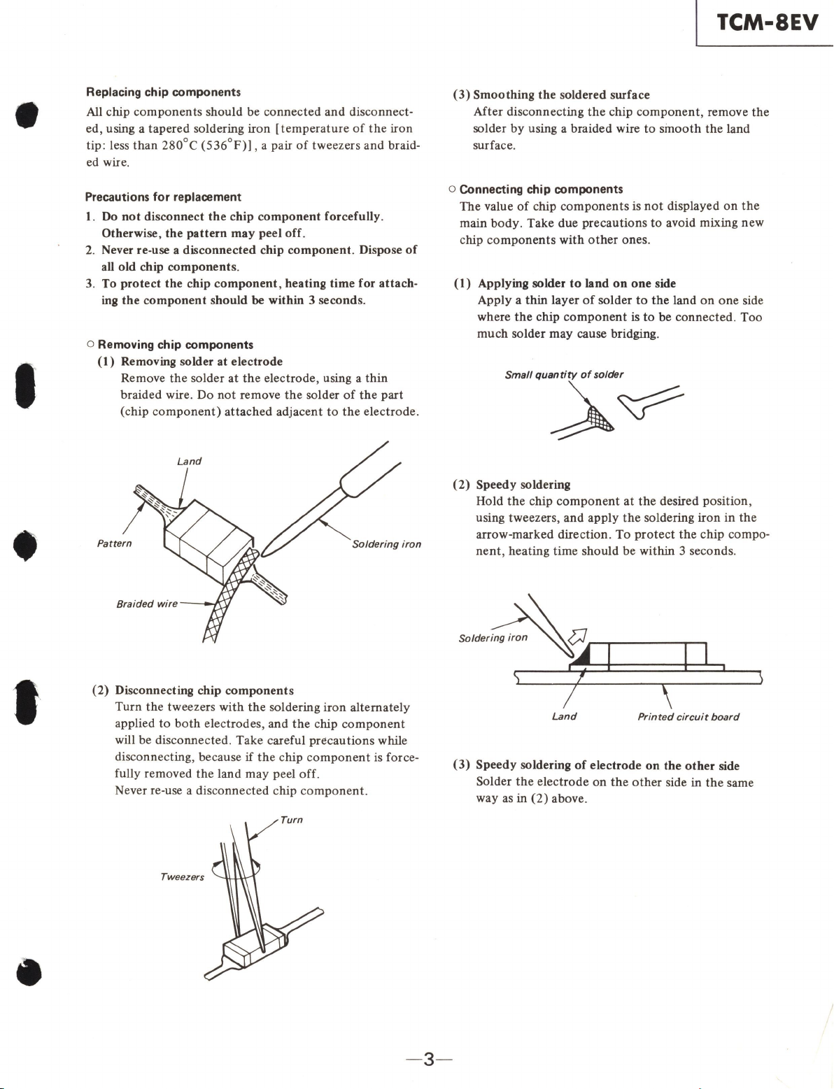
o Removing chip components
(1)
Removing solder
at
electrode
Remove
the
solder
at
the
electrode, using a
thin
braided wire. Do
not
remove
the
solder
of
the
part
(chip
component)
attached
adjacent
to
the
electrode.
Pattern Soldering iron
(2)
Disconnecting chip components
Turn
the
tweezers with
the
soldering iron alternately
applied
to
both
electrodes, and
the
chip
component
will be disconnected. Take careful precautions while
disconnecting, because
if
the
chip
component
is force-
fully removed
the
land
may
peel
off
.
Never re-use a disc
onnected
chip c
omponent
.
TCM-SEV
(3)
Smoothing the soldered surface
After disconnecting
the
chip
component
, remove
the
solder
by
using a braided wire
to
sinooth
the
land
surface.
o Connecting chip components
The value
of
chip
components
is
not
displayed
on
the
main
body.
Take due precautions
to
avoid mixing new
chip
components
with
other
ones.
(1)
Applying solder
to
land
on
one side
Apply a
thin
layer
of
solder
to
the
land
on
one
side
where
the
chip
component
is
to
be connected. Too
much
solder may cause bridging.
(2)
Speedy soldering
Hold
the
chip
component
at
the
desired position,
using tweezers, and apply
the
soldering iron in
the
arrow-marked direction. To
protect
the
chip compo-
nent
, heating time should be within 3 seconds.
Land
Printed circuit
board
(3)
Speedy soldering
of
electrode on the other side
Solder
the
electrode on
the
other
side in
the
same
way as in
(2)
above.
- 3-

www.SteamPoweredRadio.Com
TCM-SEV
Parts identification
lL~
0
0
Features
•
Voice
operated
recording
--
Recording
starts
automatically
when
detecting
the
sound stronger
than
some
extent
and stops
when
no
sound
is
applied.
•
Extremely
compact
size
for
easy one-hand
operation.
•
Simplicity
of
recording -
merely
insert a cassette and depress a
single
button
.
•
TONE
switch
to
adjust
the
tone
in
the
playback
mode
and
the
built·
in
microphone
sensitivity
in
the
record
mode
.
•
Adjustable
tape speed
in
playback
mode
.
• Cue and review
functions
to
quickly
locate any desired
portion
of
the
tape.
• One
touch
review
function
facilitates
listening
to
the
just
recorded
program.
•
Tap
e
counter
for
indexing
the
tape contents.
•
Automatic
shut
-
off
mechani
sm
activates at
the
end
of
the
tape in
either
the record
or
playback
mod
e.
0
VOR
selector
f)
SPEED
CONTROL
knob
8
PAUSE
switch
0
FF/CUE
button
0
REW/
REVIEW
button
0
PLAY
button
0 STOP/
EJECT
button
0
REC
button
0
REC/BATT
indicator
CD)
VOR
indicator
a,
MIC
jack
- 4-
4&
EAR
jack
41}
TONE
switch
41)
Tape
counter
and Reset
button
49
VOLUME
knob
4D
DC
IN
3V
jack
CD
Bui
lt-in
microphone
~
Cassette
compartment
G>
Battery
compartment
(Rear)
I
w
Speaker (Rear)
~
Hand
Strap
•
t

www.SteamPoweredRadio.Com
I
01
I
,...__
-
JIOI
~
[Mfg~
HRP
9
01
REC/PB
HEAD
51
0
4-3
REC-
PB
BIAS
OSC
0
10
1
LOW
PASS
FILTER
0201
CLOCK
PULSE
osc
IC3011
l/
21
Bt
13VI
REC
AMP
01
02
,
103
CLOCK
PULSE
INVERTER
SHAPER
02
04
-
510
4-4
REC-
PB
CLOCK
PULSE
INVERTER
SHAPER
0205
SI04
-2
REC-PB
B+
LINE
AMP
ICI
OI
(1/ 31
BBQ
AMP
02
03
5301-1
®ID
O
FF
I
LOW
f'IISS
FILTER
0202
L
I
H
VOR
SENgTvlTY
SWITCH
0306
,,,,
'
010I
•
!REC/BATT!
5101
o.[!Q@
L
-H
B+
-YVOR
ON
13
VI
SW
I
TCHING
030B
VOR
AMP
03
01
RVIOI
~
-
'3
d~
~Jl02
i='™
,,,,
0301
§ID
_l__,
LEO
DRIVE
0304
~,1
S10
4-
1
REC-
PB
OFF
-ON
VOR
SWITCHING
0303
VOR
SW
ITCHI
NG
qr!
VOR
3
ICOMPARTERI
CONTRCX.
IC30I(1/2)
0305
-
M9
01
MCT<Jl
=r
B+
1
3V
I
~
ORY
BATTERY
.r-1
SIZ
E
"AA"
IIEC
DESIGNIITION
RGI
2PCS,3V
a,
,...
0
C')
~
0
)>
C)
::c
)>
3:
0
(J)
m
C
("")
-I
-I
r
-0
z z
m
-II
....
n
3:
I
co
I'll
<

www.SteamPoweredRadio.Com
TCM-SEV
SECTION 2
CIRCUIT
DESCRIPTION
CIRCUIT DESCRIPTION
This set utilizes a
BBD
(Bucket
Brigade Device) IC
in
order
to
prevent
the
beginning
audio
from
being
recorded
brokenly
during
VOR
recording
, by delay-
ing
the
audio
signal.
Fig. 1
is
a block diagram
of
the
audio
signal delay.
The audio signal is
output
from IC101
pin@
,
passes
the
R201,
202
attenuator
and
Q201
low
pass
filter,
and
is
input
to
IC201
pin
G)
.
The
R201 ,
202
attenuator
attenuates
the
signal so
that
it does
not
go over IC201
maximum
input
level
of
about
-SdB.
LOW PASS
FILTER
0201
AUDIO
SIGNAL
DELAY
IC201
Q201
low
pass filter
operates
at
cut-off
frequency
of
4kHz
so
that
it does
not
go
over
the
clock pulse and
beat
which
operate
IC201 ,
202.
IC201 ,
202
form an
audio
signal delay 1024-stage
BBD
IC.
On
this set,
these
two
ICs delay
about
85msec
. The delayed
signal has
the
amount
attenuated
at
R201,
202
amplified
at
Q203, it passes
Q202
low
pass filter
and
is
input
to
Q
102
, 103 recording
amp
.
Q202
low pass
filter
is
to
cut
the
clock
pulse so
that
it
is
not
super-
imposed
on
the
signal
at
the
BBD IC.
AUDIO
SIGNAL
DELAY
AMPLIFIER
0203
LOW PASS
FILTER
0202
RECORD
AMPLIFIER
0102
. 103
IC202
Fig.
1.
Audio signal delay block diagram
--Pig.
2 shows
the
circuit
which
controls
on
and
off
of
the
motor
and bias oscillation during
VOR
record-
ing. The
audio
signal
output
from
ICl0l
pin @
is
amplified
at
Q301 . When
the
level
of
the
audio
signal
input
to
Q301 is large,
Q302
base
potential
drops
and
Q302
goes
on
. When this
happens,
IC301
pinG)
voltage goes higher
than
pin
Q)
and
pin
(D
goes high.
Then
Q305
,
303
turn
on
, and
supply
power
to
servo
IC
(IC601)
and bias oscillation
transistor
(Ql0l).
Q306
is
a
transistor
for switching
VOR
recording
sensitivity,
and
when
VOR
recording
sensitivity is
low
it
turns
on
and
attenuates
the
audio
signal
input
to
Q301.
Also,
when
there
is
no
audio
signal from
the
microphone,
and
the
motor
bias oscillation is
stopped
immediately,
the
last
audio
is
not
recorded
(the
audio
signal
is
delayed
about
85msec for
VOR
recording), and
further,
if
on
/
off
is
repeated
at
too
short
intervals,
the
playback
sound
will be hard
to
heas, so
C3
04
maintains
IC301
pin
G)
at
high for
about
2- 3 sec
onds
to
prevent
this.
B+ B+
c--
HEAD
AUDIO
SIGNAL
0303
TO
MOTOR
SERVO
0306
2SCl623
V0R
SENSITIVITY
SWITCH
0301
2SC623
V0R
AMP
005
0.
22
003
0.
01
R3
06
1k
O0
G
R305
0.
001
llk
R307
81
R
308
470,
0302
2SAll62
V0R
SW
I
TCHING
R310
I0k
R3
09
4
7k
+ C304
4.7
,
ov
IC3011l/2l
NJM2903M
V0R
S
WITCHING
IC
0
MFIIRTER
I
Fig.
2.
Motor,
Bias
oscillator control circuit
-6-
2SAll62
BIAS
OSCILLATOR
0303
V0R
SW
ITC
HIN
G
CIRCUIT
0305
2SCl623
V0
R
CO
NTR
OL
•
I
•
I
•

www.SteamPoweredRadio.Com
I
•
I
•
SECTION 3
DISASSEMBLY
Note
.
Follow
the
disassembly
procedure
in
the
numerical
order
given.
REAR
CABINET
f)
+PTP1.l x 6
(TYPE
2)
f)
+PTP1.l
x 6
(TYPE
3)
i
0
Remove
the
rear
cabinet.
f)
+PTP1.7 x 5
(TYPE
3J
@
Remove
the
control
panel.
TCM-SEV
f)
+PTP1.7 x 6
(TYPE
2)
j
i
f)
+PTP2
x
10
(TYPE
2
i
NON-SLIT)
0
Remove
the
battery
lid
.
AUDIO
BOARD
0
+PTP1.4
X
3
f)
Unlock.
-7-

www.SteamPoweredRadio.Com
TCM-8EV
SECTION 4
ADJUSTMENTS
4-1.
MECHANICAL
ADJUSTMENTS AND
MEASUREMENT
PRECAUTION
I. Clean
th
e following
parts
with a de
natured-
alcohol-moistened swab:
rec
ord
/
playback
head
erase head
capstan
pinch
roller
rubber
belts
idlers
2. Demagnetize
the
record
/
playback
head
with
a
head
demagnetizer.
(Do
not
bring
the
head
de-
magnetizer
close
to
the
erase
head.)
3. Do
not
use a magnetized screwdriver for
the
adjustments
.
4.
After
the
adjustments,
apply
suitable Jocking
c
ompound
to
the
parts
adjusted.
power
s
upply
voltage : 3V de
SPEED
CONTROL
knob:
center
click
Torque Measurement
Torque
Meter
Reading
Forward 27 -
48
g-c
m
(0.37 - 0.66 oz-inch)
Fast
Forward
55 -
75
g
-cm
and Rewind (0.76 -1.03 oz
-in
ch)
Back Tension 2 - 4 g
-c
m
0.027 - 0.055 oz
-in
ch)
Tape
Tension Measurement
Meter
Meter Reading
Torque Meter
CQ-102C
CQ-201B
CQ-102C
5.
The
adjustments
should
be
performed
with
the
rated
power
supply
voltage
unle
ss
otherwise
noted.
CQ-403A More than 100 g (3.53 oz)
Head
Height Adjustment
power
supply
voltage:
3V
de
Procedure:
1.
Prepare an
adjustment
cassette as
shown
below.
tape cassette
Cut
out
hatched
portions.
2.
In
record
mode
and viewing from
the
front,
adjust
the
head heights
to
eliminate
tape
curl
and
tape
twist
at
arrowed
portions.
~
erase
head
record/playback
head
~-Fl
'"'Ejj -
/~
3-578-138-01 (t=0.1)
3-578-138-11 (t=0.2)
Shim,
head
height
adjustment
(-'1
..
~
11~
-10
-
I
•
t
•

www.SteamPoweredRadio.Com
••
I
I
•
4-2.
ELECTRICAL
ADJUSTMENTS
Record/playback
Head
Azimuth Adjustment
Settin
g:
VOLUME
knob:
SPEED
CONT
R
OL
k
nob:
center
click
center
click
Procedure:
1.
Mode: pl
ayback
test tape
P-4-
A063
(6.
3kHz
, -
10d8)
s
et
VTVM
earphone
jack
2.
Tu
rn
th
e adju
stme
nt
screw
to
obtain
the
maxi
-
mu
m
readi
ng
on
VTVM.
Note:
Several peaks
may
appear, but take the
max
i-
m
um
.
3.
After
the
adjustme
nt, l
ock
the adju
stme
nt
screw
with
s
ui
tab
le l
ocking
co
mp
o
und
.
Adjustment Location:
headazi
muth
adjustment
screw
TCM-BEV
Tape
Speed
Adjustment
Setting:
VOLUME
knob:
SPEED
CONT
ROL
knob:
center
click
center
click
Procedure:
Mode:
playback
te
st
tape
I--VS
-
48A
(3kHz
, OdB)
Specification:
Speed checker
±2
%
speed check
er
LFM
-
30
or
di
gita
l
frequ
e
ncy
counter
10kn ~
k
=::!..l-'
i
i;JJ
earphone
jack
Digital frequency counter
2,
940 - 3,
06
0Hz
Fre
qu
ency difference b
etwee
n the beginning
a
nd
the
end
of
th
e t
ape
sho
uld
be wit
hi
n I%
(30
Hz).
Adjus
tm
ent Location:
•
---1
-
11
-
adjustable
resistor

www.SteamPoweredRadio.Com
TCM-8EV
Record
Bias
Adjustment
Procedure:
1.
Mode:
record
record
portion
set
set
EXT
MIC
1)
1kHz
}
2)
6.
3kHz
llµV
(-
80d8)
earphone jack
Play back
the
tape
recorded
in
step
1.
blank tape
CS
-10
Adjust
the
VOLUME
control
so
that
VTVM read-
ing
is
0.25V
(-
I0dB
)
when
!kHz
is
played
back.
Next
play back
6.3kHz
and
check
that
the
level
difference
at
this
time
is
within
±3dB.
If
not,
connect
or
disconnect
patterns
" and
@
and
repeat
step
1
and
2.
Adjustment Location:
Audio B
oard
UR60i7
"LU.....J
f'I
Pattern connection
" @
"
@
6.
3kHz
VTVM
reading
down
t
up
Microphone Sensitivity Adjustment
Wh
en replacing
the
microphone,
perform
this adjust-
ment.
Mark
of
Microphone Pattern Connection
BLACK
@
RED
~
Adjustment Location:
Audio B
oard
Cl
l8
<>-:pt-<>
eg
-
12
-

www.SteamPoweredRadio.Com
BBD Circuit Bias Adjustment
power
supply voltage: 2.1 V de
Procedure:
VOR recording
mode
af
osc
fol,
amou,<o,~
1
TOkn.
...----.
U O O O !________
set
600n.
MIC
JACK
TkHz
0.llmV
(-60d8)
Apply a IkHz, 0.
77m
V (- 60dB) signal
to
mic
jack
and place
the
set in
VOR
recording
mode
.
VOR
Board
(Side
A)
Adjust
the
tap
connection
to
obtain
normal sine
wave
on
the
oscilloscope. If
the
adjustment
is
not
correctly
made
sine wave will be clipped.
Adjustment Location: BBD Board (Side A)
adjustment
tap
RED
0203
~
ct]
N
UN
TCM-SEV
VOR LED Brightness Adjustment
power
supply voltage: 2.SV de
Procedure:
Place
the
set in
VOR
recording mode.
Adjust
the
resistance value so
that
the
VOR
LED
is
brighter
than
REC/BATT LED a little.
The
power
value
is
Skfl
- 1
0kfl
.
Adjustment
Location:
VOR
Board (Side A)
adjustment
resistor
Chip resistor (1/10W)
Resistance value Parts No.
5.
lk
1-216-066-00
5.6k
1-216-067-00
6.2k 1-216-068-00
6.8k
1-216-069-00
7.Sk 1-216-070-00
8.2k
1-216-071-00
9.
lk
1-216-072-00
!Ok 1-216-073-00
-13-

www.SteamPoweredRadio.Com
~
TCM-BEV
1
A
B
C
D
E
G
J
0
IC
5-1. MOUNTING DIAGRAM
2
IC202
IC201
3 4
203
IC202
I
C201
[BBD
BOARD]
IB
SIDE)
'
[VOR
BOARO)[A
SIDE)
[
BBD
BOARD
(.A
SIDE
l
\
[VOR
BOARO](B
SIDE)
\
[SPEED
CONTROL
BOARD](A
SIDE)
-
14-
SECTION 5
DIAGRAMS
5 6
301
306
304
7 8
302
m:308
303
305
9
10
11
202
IC301
204
205
\'OR
REC
MOOE
10
""'
flhh~
,,
-,
\'OR
REC
WOIJE
n
fUU1
J.,,
_,
_j
T-CM-BEV
12 13
14
15
20
1 6
01
IC6
01
30
1
[L
ED
BOA
RD]
• J''U'? :
co
mp
on
ent-side pattern.
• ,},f/:J : B +
pa
ttern
•
-+-
:
signa
l path
•
---
· :
Throu
gh
ho
le
connect
i
on
.
TCM-BEV
16
101
103
102
17
18
19
ICI0I
20
21
22
23
0 ·-
IC A
10
2 D
IOI
CNIOI
~
TOT
AL
CURRENT
B
FWD: 1
07mA
FF
:
93
11
A
REW
:
II
Om
A
REC
: 119mA
C I
D
E •
F
G t
H
J

www.SteamPoweredRadio.Com
•A
B
C
D
E
F
I G
H
J
TCM-BEV
TCM-BEV
5-2. SCHEMATIC
DIAGRAM
• Semiconductor
Lead
Layouts
1
16
1
2 3
~
MI
C901
C-
100
7A
BUI
LT
IN
MI
C
~
II
H
RP
901
ell>
PP
l
34-3GT
RE
C/
PB
HEJi)
HEso,
~x
1
EBF
H6
..::._J
E
RAS
E
f£AO
4
(AUDI
O
BOARD]
MICRO
P
HON
E
I
SE
NSI
T
IV
I
TY
--
/1.
_
~
~\
<>-c
r,
RIO
I
CIOI
680
0.4
7
•
sov
RI02
b_
~~
!
~
1.
2k
'...+.
SOV
,.
___.
~
: :
(
Cl
41
0.
001
5
6
.....
-,-
23
V
'
7
O
.lV
C
/0
7
10.
35\1)
I
,
r:r.
~-
v_._
,,
8
ICIOI
CX807
REC/
P8
A
MP
9
0
102
IT22
RE
C/P
BS
ELE
C
T,
SPE
AKER/EARP
H
ONE
8140
.
001
•
I.I
V
.,_
I
CIO
l
11/
l l
I.I
V~
t-
-<,ll--+
-I
VOl
.R
EG
+
-
8~
R/1
7
------
•10
LI
NEMllf'
Ll
!>V
,,
.....
...
AG
C /
2V
L
ED
DRIV
E 6
10
0101
S
LB
23U
R27
.,.,+,
..
~
C
II
O
4.7
25V
R
II
S
1111/lllrl
~'?1
~
sov
H
.....
...,..
RV
IOI
1
0k
~
11
R/14
3.
311
12
2.
lV
•
,..
iv
l""""I
~7
-
Cl!~ ;
0.22
RIP
P
LE
FILTER
50V
Rll3
/.4V
2.2111
/
IWl
+
.....
.
..
~
CIII
0.
22
so
v
13 14
15
-I II
~v
tl.
C
/1
9
l
210
I
4V
~
,..
1.
4v.....
..
.....
G:)
7
...
SP90
1
,..
1.
•v
SPEAKER
e
H
i~~:~
I
_.
UV
[',
SEREC
T
I
II
.
..
,.•v
.,-·
EARPHONE
AMP
--
3V
II
~
e
LJ=
ICIOl
11/
31
t
--:=::::
•
=~
!=
JI•
POWES
I03R
uv
~
3
~
s101 0
~~
==
-
::
_c
00
1
30
22
~~•~
ci
}•
,~
~~
6
I I
TO
TAL
CVR
E
NT
uv•
lo.6v•s ' 6
ll2HEI
o.
•v .
.1
~
FW
0·1
01
111A
1-
--
R
"'
,
!ili"'o
---+---i
crJ!'--
C/35
: ~
=~
C/26
::1~
1~8
L- H
j
~~:
ro
'
b~
CJ
lt
I _~ ~
\:
:!:
t
R/
09
3
90
0
J~
0.
001
;i~,
;vT
0·
0068
"•
7
6k
T
,
tv
voR
REc
:1
31
A
..----+----_...,_..,.
_____
.;..._.
_____
...,__
....
...,.--
■-
■
------.------------...,--+---+---------------
■--...,---...,_
____
..,.;,;;,,;;,,;;,
··
....,_...,_
___
...,._.~-
■
+-.....
-!-
SIZE
AA
~y
l
.i:1
S10<
·3
SPEED
CONTROL]
Cll
8
::
T'IEC
DES
I
GNA
TI
ON
R
6l
RE<:
..
PB
,._
1-~-
-,
R"'12,.,i
""
1,.,2•
:..,--;"1
t-L+~
~~~
L6
_5~
.,__
;0
;;;
1o
~i
,.
•_
3v
"""'
__
__
B_O_A_R_D_(_l_/_3_)_
____
r-
-t--------
-
-1-------------
--
3
-;
v•
--~
:'.".""
---------
-
--
~
----1
0.
00
1
~--+--<
>--~
2PCS,3
V
00V
Clll
25
V Rl2I
4
v-'
~
Cll6
I
~
~
MOTOR
DR
IVE
/A
Cl
8.
7/
v-
c,22
I
--
I
cii1
v-
l\_JI
R
ll9
060
1
Q
•
l.
◄
SV
1
-: 5v
r
____
7
o.
0033
u .\
102
~
•
101
o:!2
~
.II
~
o:r
I
T
.•v _,.
,
.
◄
sv
I
~
1TIOI - · ..,.-.,
l6
+ - - l IC
GOI
'7
8
I
(!)
M9
01
=
~~u
W
rn
~,~
~~
~
--f
1~~
J
REC
BIAS
osc
~,2
l
~V
V
~
~
;~
}
flv
~
: H
M
~~
~:
l~
E~VO
J
fuj
IC
60
~1
~
...J.--:i-
0
~
~R~
T
~:i·
Cll2
=
Rl26
3V
RIN
,· ~ ~
·-~
~·
-
T l ---.j.,
~-
1
}-
~-
•0V
----~
-
+-
-.--
+-
-(
1-----'
0.006l
IOk
l
/.
7VI
, +
Cl2
1
I'?
;s
4
lv
REC 1
2•
I.
JV
~ I
I
R606
SI0<-
1
--11
~
REC
4-
P8
,.._
_.
l
_,
Y
.-
1-\-f"'-..
01
01
BIAS
82
e>-
-W,
- ~
--
-+---<.-
-f-
---{l
')------
r.
lirnii<im
'!'
..
~RENCEI-+
--
~
:2
l-2.3VI
2
W !
,~
i
V
TA
◄
.
3/1
0101 I
OV
I
01
02
0 1
03
S104-4
s"\..-..../5~
3)--
n l
H60~
2SC
l6
23 2SCl623 2
SA
ll62
REC-
PB 0.6
v·
T · o.
2v
\6
Jb7
t
'
j
J
-
t
I
RV6
01
-~
RV602
I
20k
ISf'EED~
--
R
60
1
2.7
TH
P60<
BI
AS
OSC
--REC
AMP--
n r
S1
02
:!I..
C
602
A..-.
,..._
~
T
I/
SOV
R~3
+
~
601
,,_.
v-
-~- F
-_
o_•
____
_.
__
...,_
__
-+,,;;,
ll.t:_w_l
__
;
..,..
~~~
--,._-
+
■
-
1
■--
~
h,,.
(SPE
ED
CO
N
TROL
]
......
BO
ARD0/
3)
'"
I
·'
..
'
,._
...-
(L
ED
BOARD
1----_
,
--------------
■■■
<
l--
-_ ..........
~-----------i,-~---4
-
[VOR
BOARD]
1
C20
1
-----■
-(-B_B_D_B_O_AR_D_]
_____
1_c
2
_0_1
,-2
0-2--
,
------
R201
1
01
L
MN3307
...-
AUOl'.l
SIGNA
L
OELAV
020
3
2SC
l623
8
80
AMP
<3V
>
...
----+-----
1£-
1!~)
C3
VJ
0
309
0308
1
8~
1
2SCl623
2SA
ll
62
<l
Vl
3v
[
SP~~~Nc;~
L-]
~
S0.047
C217
' ~
:~
IOOp
R204
3.31
_,_
R206
270k
R207
"
R232
lk
(l
~V)
._
(
JV
)
t~
20
8
(1
5Vl
't
k I
I ~
fm
I
C2
01
~
r
R21
0 I
C2
02
L
,--.-
-
~-t=
'l:
"~+-w.+--~-~
-
-,
t J
~
(3
.
2V)
~h
C202
R230
l4V
C219
l.l
k
~i~
3,
~~
<2
.
2V>.
020
1 C
206
<l
•V
)
U9Y
>
C21
0
<1
9V
)
220,,
330k
0047
•
H
(3
2V
h
100,
i(,,
R231
R
202
•20s
,
;::w
1
\.
""1
....,,,
o.p,
47
~
~102HTEP
I • -
0
11!'
7
I
1024
sT£P
I /
.•
/;:>< 0
20
3 ·
~
7.
Sk
3.
3k
,
1.
',~~V~)
.---1-,-.,~>+-~-
l
..
l-t---T'
"l.-2
-{
V)l 880
I
7 - ..
I / \ I
1
1.
4V)
3
.-l
BBD
I
cii
2
--V
((l
8~)
\!>
'---(
I-R"'2"'16-+--1
1
,-..VR2"'
11
...-
(1-.
lV1
- -
H\...._,
02
02
,,
o
1/
\ 9 '
I - ~
~
0.047
~
<0
.
25V
)
3.31
3.
31
®°
ci/
13
c~s
, ,
e
R212
C~-
::
0_
027
•v
1 , /
56k
<3.
2v
1 c2
zo+
c2
1•
·
/.
/ !5l '\.
R214
R228
I 10·~
0.0
33
: =l68t2
R208
roo
ra
~
<L
4V) 2
r'
~
~
-
-\I
~l-"'l_l)j
-~
561
1k
4V :
oc
.
00
◄
2,s,
R22
.21
9.
R2
23
62k
2.2k
L_ll_
AS
R~
R2~
22
<l4V
r-
I
I
O<l
a~g
0201
2SCl623
LO
W
PASS
FI
L
TER
R22
2
100,
, I f
- -
-------
-
----+------
,
------
-
______
_,
O V)
VOR
REC
M
ODE
ro,,.
1
Rl20
2
k•
R3226
C207
(R229
II
30
220,
330
-n n
n-.
R319
6.
Sk
02
02
2S
Cl623
LOW
FaSSF
I
LTER
Rl03
~
2.
2,
C
305
OJ2
w,i
.,-ii-:-,
usv,
____
_,..
- -J u u
L~
~t
·
''~
c~1121
L ,
Hh
'
,,..
L•
_,
v.;;
''
•
""'
=--'
_,.I-:--
~-
--
-,-
.l
ttrt"'
020~
~
5
I I
.t:.fJ
020
R,~.2.'
<0.
4V
)
~
R3
52 Cl02
~'ll2,.~f
i'
.9Vl
22,
<
ov
1
R3
20
R301
IOOp
-
_
_,;
•
.....,,
'·
,.,.
5
•
,_.-
Kl,.,.k
--t"
l
t-<
.,__,.._
,
tt
rt"'
030
1
11
R
306
-j
f-
----'
IV
) "-.
R22~:
(0.4V~
VOR
RE
C
MO
DE
•
"'\.
=
10,,..
R23l
Q2V
VOR
R
EC
MO~
r--,
IOI
C2
16
.:
R
22
1
·n n
n~P
·' n n n
---i
_j
2.
8V,-
p
220,,
·
270k
j LJ LJ
L__j
'
j
LJ
LJ
L
I
C301
ll/
2l
02
04 , 205
<OSVl:V
OR
L•
030
6 0.
047
<0.5
v>
...._,.
Lf!:
do
,
\..._,
<OV> :
't'OR
H
0306
2SCl
62
3
1k
/
B
OA
RD
(l
/3)
.
Q:&
I I
2.8Vl
2.8Vk2
.
2Vl
•
.....,,,.,_
_,_,
( R~l
R35'
:~(
~
:I
Off
7 ~
5~
1 2
.8Vl2B
VK0
l~. "
I
O V
(
■
~
I
030
1
tr
,.,- 0-V
-.-t
-<t
0309
IN (
I.
M
7
H
_.
I
OVl
1
i"
1v
1 I
r r
10
.
61
I
;
g~
~
~ ' i1
5
~
:"
\ ~
Rl
15
J
~
12.
lYI
- - -
<OV>
030
4
2SCl
623
LED
DR
I
VE
OlO
◄
L
EO
1
BRIG<T
0
30
1
S
LB
2
3UR27
0307
OTCll4YK
VOR
ON
SW
IT
CH
ING
R3
55
IOk
'
lV
/3VI
)
rv
i
0303
2S
All
62
'
~
0303
Rl
/4
!
K
J.
/O
I
L
✓
sw
,~
g:
,
NG
I
Rl12
~·
030
2
IC
30
Hl/2l
2S
Al
l6
2
NJM
2
903M
,
0
305
2SC
l623
VOR
CO
NT
ROL
NJM29
0
3M
2
SC
l623 (
_ _
________
c
L_
o_
cx
_
PIA.
_
SE
0Si,_
C
LO
CK
PIA.SE
IIIV
ERTER,~PE
_R
_____
,
__
f
_______
_
VOR
SENSITIVITY
SWITCH
0
30
1
2S
C623
VO
R
AIIP
_
vo
_R_
sw
_1
Tc
_H_1N_G
_____
VOR
_ s_w_,rc_HIN
~O
M_
JU
_T_E_
Rl
________
....
-
17
--
18
-
17
18
A
B
C
D
E
F
G
H
J
Note:
• All capac it o
rs
are
in
µF
u
nless
otherwise
no
t
ed
.
pF
:
µ.µ.
F
SOWV o r
less
are
no
t
indicated
except
for
elect
ro lyt
ics
and
tanta
l
ums
.
• All r
esi
stors
are
In
ohms
,
1/1
OW
unless
ot
herwise n
oted
.
kn
: 1
ooon
,
Mn
: 1
0OO
kn
• • :
selec
ted
to
y ield op
tim
u m
perfo
rma
nc
e.
• c:::::J :
ad
ju
s
tm
e
nt
fo
r r
ep
a
ir
.
•
---
:
B+
bus.
• Vo lt
ages
are d e
wit
h r
espe
ct
to gro
und
un
l
ess
oth
erw i
se
·
no
ted
.
•
Re
ad ings are taken u
nde
r
no
-s
i
gna
l c
ond
it i
ons
w it h
a V O M
(
DC
50
k
S1
/V
).
no m
ark
:
PB
( ) :
REC
<
>:
V
OA
REC (
TAPE
ST
OP
)
{ } :
VOA
_
REC
(
TAP
E
RUN
NI
NG
)
• Vo lt
age
v
ar
iat
ion
s m ay
be
noted
d ue to
nor
m al p r
odu
c•
t i
on
to leran
ces
.
•
AC
volt
ag
e r
ead
i
ngs
in
the
bias
osc
i
llato
r w i
th
a VTV M.
• T o ta l c
urre
nt
is
me
a
su
r
ed
with
no
casse
tt
e i
ns
talled .
•
Sw
i
tc
h
Ref. No. Switch
Po
si
tion
S
101
TONE
L
S
10
2
PAUSE
OFF
S 103
POW
ER
OFF
S
104
REC
/
PB
PB
S30 1
VOA
OFF
• • :
signa
l
path
.
(PB)
• 1$ -:
signa
l pat h.
(VOA
REC)
Note:
Vo
ltages are meas
ure
d w
ith
a VOM (5
0k
n/V)
.
5-3. SEMICONDUCTORS
TCM-BEV
AN
86
12
S
CX
8
07
NJ
M2
903M 1T22A
MN
330
7
n+1
"~~~ D
.'/
n+1
slit
or ··
dot 1 2
n
sl
it
or
do\ ..--
'L.:.-..J
cathode
{.,
,
oo
(T
op
vie
w)
SLB
·
23
U
R2
7
cathode
anode
-1
9-
2
S8
7
39
t
E C B
2S
A1162
2S
C1623
DTC114YK

www.SteamPoweredRadio.Com
TCM-SEV
1
(1)
A
B
C
D
E
F
G
H
41
J
2
EXPLODED V SECTION 6
IEWS
AND
PARTS
LIST
3
30
18
31
14
4 5
6
40
15
~
)3
'
C
l',o\
,
/
..
-.:::;
~ ~
MIC901
:i1::~~u~
·
Y~
~
@ ' .
~36
~
43 ,
4
I
20
I
1
31
(l,
50
;f:J,'
~P
l
28
~
,,
.,)
1/
n
~
-,,
$
('
'
'
t"s
,,
~ , /
..
""1
f
;,--
2
.•
24 33
8
-
20
-
7
(2)
A
B
C
D
E
F
G
H
J

www.SteamPoweredRadio.Com
TCM-8EV
GENERAL
SECTION
No.
Part
No.
Description
1
•••..•••••••
2 6;3-311-853-01
CONDUCTOR,
GROUND
3 3-318-201-21
SCREW
(B)
(1.4X5),
TAPPING
4 3-318-202-01
SCREW
(M3)
(1.4X3),
TAPPING
5 3-318-203-01
SCREW
(1.7X6),
TAPPING
6 3-318-203-11
SCREW
(l.7X6),
TAPPING
7 3-318-204-31
SCREW
(Ml.7X6),
TAPPING
8 3-318-204-61
SCREW
(Ml.7X5),
TAPPING
9 3-318-205-01
SCREW
(l.7X2.5)
10
3-318-209-01
TERMINAL
BOARD,
PLUS
11
3-318-210-01
SPRING
12
3-318-211-01
SHAFT,
CASSETTE
13
3-318-214-01
ARM,
TOGGLE
14
3-318-215-01
SPRING
15
3-318-216-01
CUSHION,
MICROPHONE
16
3-318-218-11
STRAP,
HAND
17
3-318-225-01
KNOB,
SPEEO
CONTROL
18
3-318-226-01
LEVER,
EJECT
19
3-318-227-01
KNOB,
PAUSE
20
3-318-231-21
CABINET
(REAR)
21
3-318-311-01
SHEET,
CONDUCTIVE,
MIC
22
3-318-312-01
SHEET,
CONDUCTIVE,
SP
23
3-318-314-01
SPACER
24
3-318-315-01
KNOB,
CONTROL
25
3-318-323-01
RING,
RETAINING
(3)
26
3-318-327-01
SPRING,
TENSION
27
6;3-318-328-01
SHEET
(A),
INSULATING
28
6;3-318-339-01
SHEET
(E)
CONDUCTIVE
29
3-649-266-00
PIN,
PARALLEL
30
3-703-357-06
PIN,
PARALLEL
(DIA.
l.6Xl4)
3-831-441-XX
CUSHION
7-623-203-11
SW
1.4,
TYPE
1
31
32
33
7-685-106-14
SCREW
+P
2Xl0
TYPE2
NON-SLIT
34
35
36
37
38
39
40
41
42
43
NOTE:
9-911-841-XX
CUSHION
9-911-840-XX
CUSHION,
RUBBER
9-911-844-XX
CUSHION,
SPEAKER
9-911-863-XX
PLATE,
BLIND
A-3046-031-A
BATTERY
LID
ASSY
X-331B-218-1
LID
ASSY,
CASSETTE
X-3318-219-1
CONTROL
PANEL
A
SS
Y
X-3318-220-1
CABINET
ASSY
3-318-341-01
SHEET
(B)
INSULATING
The
mechanical
parts with
no
reference
number
in
the
exploded
views
are not
supplied .
CAPAC
I
TORS:
MF
:uF
,
PF
:uuF.
RESISTORS
No.
81
82
83
84
85
86
87
88
89
90
91
91
91
91
No.
301
302
303
304
305
306
307
308
309
310
311
312
313
314
315
316
317
318
319
320
321
322
323
324
325
326
327
ACCESSORY
&
PACKING
MATERIAL
Part
No.
Description
3-318-344-01
INDIVIDUAL
CARTON
1-504-059-11
MAGNETIC
EARPHONE(ME-20H)
3-314-036-00
SPACER
3-318-305-01
CUSHION
3-318-335-01
CASE,
CARRYING
3-570-631-81
BAG,
POLYETHYLENE
3-
701-624-00
BAG,
POLYETHYLENE
3-701-999-00
LABEL,
SERIAL
NUMBER
3-
703- 710-01
STICKER,
SONY
SYMBOL
(12)
3-
793-828-11
QUESTIONNAIRE
3-773-823-11
(AEP,E)
•••••••••
MANUAL,
IN
STRU
CTI
ON
3-773-823-21 (US,Canadian)
•••
MANUAL,
INSTRUCTION
3- 773-823-31 (Canadian)
••••••
MANUAL,
INSTRUCTION
3-773-823-41
(AEP)
.••..••....
MANUAL,
INSTRUCTION
MECHANISM
SECTION
Part
No.
Description
1-548-541-31
COUNTER
3-306-836-02
CAP,
REEL,
T
3-318-201-01
SCREW
(B)
(l.4X3),
TAPPING
3-318-208-01
BUTTON,
STOP
3-318-220-01
KNOB,
CONTROL
3-318-221-01
BUTTON,
REC
3-318-222-01
BUTTON,
PLAY
3-318-223-01
BUTTON,
FF
3-318-228-01
BUTTON,
REW
3-31B-236-0l
WASHER,
POLY,
SLIT
3-318-237-01
SPRING,
COMPRESSION
3-318-238-01
SPRI
NG,
TENSION
3-318-239-01
BELT
3-318-240-01
SCR
EW
(1.4),
SPEC
IAL
3-318-241-01
SPRING,
COMPRESSION
3-318-242-01
BELT
3-318-243-01
SPRING,
TENSION
3-318-246-01
SPRING,
TENSION
3-318-247-01
SPRING,
TENSION
3-318-248-01
SPRING,
TENSION
3-318-249-01
SPRING,
TENSION
3-318-250-01
SPRING,
TENSION
3-318-251-01
SPRING,
TENSION
3-318-252-01
ARM,
DETECTION
3-318-254-01
CUSHION,
MOTOR
3-318-265-01
GEAR
(B),
FR
6
;3-318-267-01
LEVER,
CR
Items
marked
" 6 " are not stocked since
they are
seldom
required for routine
service.
Some
delay should
be
antici
-
pated
when
ordering these items.
· A
11
resistors
are in
ohms
.
Due
to standardization,
parts
with part
numbers
(6-
666
-
666
-XX
or
6-
6666
-66
6
-X)
may
be
different
from
those
used
in the
set
.
• F : nonflanmible
COILS
·
t+IH
:
mH,
UH
: uH
SEMICONDUCTORS
In
each
case,
U:
µ,
for
example:
UA•••:
u
A···,
UPA
·••:
µP
A·
··,
UPC·••:
µPC
,
UPD
· · · :
uPD
· · ·
-24-
Other Sony Cassette Player manuals

Sony
Sony TC-K333ESA User manual

Sony
Sony TC-WA8ESA User manual

Sony
Sony Walkman WM-FX493 User manual

Sony
Sony Walkman WM-GX788 User manual

Sony
Sony TC-K909ES User manual

Sony
Sony WM-PA1 User manual

Sony
Sony TC-K333ESG User manual

Sony
Sony CFM-A50 User manual

Sony
Sony TCS TCS-30D User manual

Sony
Sony TC-WE405 User manual

Sony
Sony Walkman WM-GX788 User manual

Sony
Sony WALKMAN PROFESSIONAL User manual

Sony
Sony WM 701C User manual

Sony
Sony XR-CA370X User manual

Sony
Sony TCM-313 User manual

Sony
Sony CFM-10 Operating Instructions (primary... User manual

Sony
Sony Walkman WM-FX477 User manual

Sony
Sony Pressman TCM-16 Instruction Manual

Sony
Sony Walkman WM-FX522 User manual

Sony
Sony TC-FX211 User manual