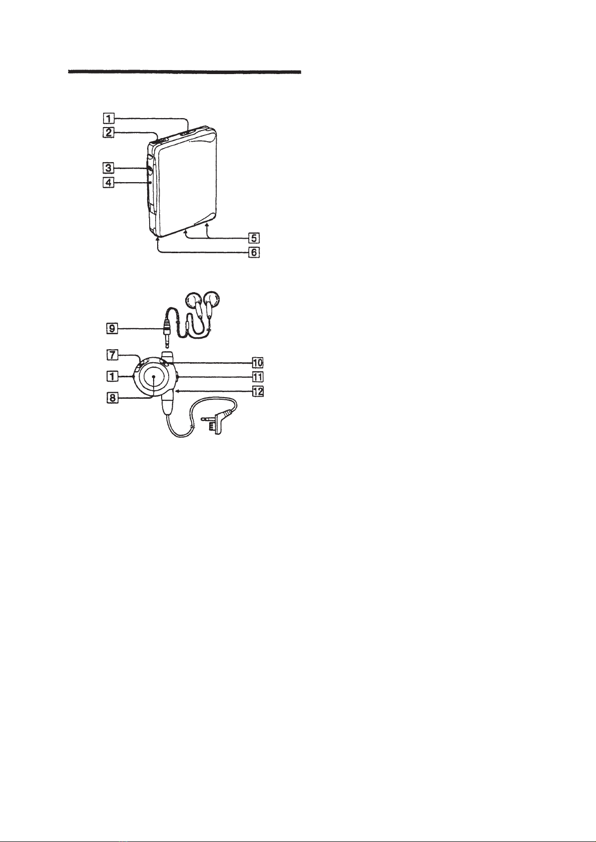
Sony Walkman WM-EX9 User manual

– 1 –
Model Name Using Similar Mechanism NEW
Tape Transport Mechanism Type MF-WMEX9-162
SERVICE MANUAL
US Model
AEP Model
UK Model
E Model
Tourist Model
WM-EX9
CASSETTE PLAYER
System Compact cassette stereo
Frequency response (Dolby NR off)
Playback: 30 - 18,000 Hz
Output Headphones 2jack
Load impedance 8 - 300 ohms
Maximum output level 4 mW + 4 mW (32 Ω)
Power requirements DC 1.5 V
Nickel metal hydride rechargeable
battery (supplied)
One R6 (size AA) batteries
(negative ground)
Battery life (Approx. hours)
Rechargeable NH-14WM 40
fully charged
Rechargeable NC-6WM 18
fully charged
Sony alkaline LR6 (WM) 60
Rechargeable NH-14WM 100
Sony alkaline LR6 (WM)
used together
Rechargeable NC-6WM 78
Sony alkaline LR6 (WM)
used together
Dimensions (w/h/d) Approx. 77.7 ×108 ×19.6 mm
(3 1/8 ×4 3/8 ×25/32 in.)
projecting parts and controls
Mass Approx. 140 g / Approx. 205 g
(5.0 oz/7.3 oz)
incl. rechargeable battery
and a cassette
SPECIFICATIONS
DolbynoisereductionmanufacturedunderlicensefromDolbyLabo-
ratories Licensing Corporation.
“DOLBY” and the double-D symbol aare trademarks of Dolby
Laboratories Licensing Corporation.
MICROFILM
Photo: Gold type
Ver 1.1 1999. 01
Supplied accessories Battery charger BC-7DC (1)
(US model)
Battery charger BC-7DY (1)
(AEP, French model)
Battery charger BC-7HT (1)
(E, Tourist model)
Battery charger BC-7S (1)
(UK model)
Battery charger BC-9HR (1)
(Korea model)
Rechargeable battery NH-14WM (1)
(E, Tourist, Korea model)
Rechargeable battery NC-6WM (1)
(Except E, Tourist, Korea model)
Rechargeable battery case (1)
Dry battery case (1)
Stereo headphones with remote control
MDR-ED132SP + RM-WME21L (1)
Carrying pouch (1)
AC plug adaptor (1) (E, Tourist model)
Design and specifications are subject to change without notice.
Ver 1.1 1999. 01

– 2 –
TABLE OF CONTENTS
1. SERVICING NOTE
1-1. Service Mode ...................................................................... 3
1-2. Rotational System ............................................................... 4
2. GENERAL
Location of controls................................................................. 5
3. DISASSEMBLY
3-1. Cassette Lid Assy ................................................................ 6
3-2. Case ..................................................................................... 6
3-3. Ornament (Open) Block Assy ............................................. 7
3-4. SUB Board, Leaf Switch, MAIN Board ............................. 7
3-5. Belt (F1), Motor (F1) (M701) ............................................. 8
4. MECHANICAL ADJUSTMENTS..............................9
5. ELECTRICAL ADJUSTMENTS ...............................9
6. DIAGRAMS
6-1. IC Pin Description............................................................. 10
6-2. Block Diagram .................................................................. 11
6-3. Printed Wiring Boards (Board suffix No. : -11) ................ 13
6-4. Printed Wiring Boards (Board suffix No. : -12) ................ 16
6-5. Schematic Diagram ........................................................... 19
7. EXPLODEDVIEWS
7-1. Case Section ...................................................................... 24
7-2. Mechanism Deck Section.................................................. 25
8. ELECTRICAL PARTS LIST.....................................26
Flexible Circuit Board Repairing
•Keep the temperature of the soldering iron around 270˚C during
repairing.
•Do not touch the soldering iron on the same conductor of the
circuit board (within 3 times).
•Be careful not to apply force on the conductor when soldering
or unsoldering.
Notes on Chip Component Replacement
•Never reuse a disconnected chip component.
•Notice that the minus side of a tantalum capacitor may be dam-
aged by heat.
SAFETY-RELATED COMPONENT WARNING!!
COMPONENTS IDENTIFIED BY MARK !OR DOTTED LINE
WITH MARK !ON THE SCHEMATIC DIAGRAMS AND IN
THE PARTS LIST ARE CRITICAL TO SAFE OPERATION.
REPLACE THESE COMPONENTS WITH SONY PARTS WHOSE
PART NUMBERS APPEAR AS SHOWN IN THIS MANUAL OR
IN SUPPLEMENTS PUBLISHED BY SONY.
ATTENTION AU COMPOSANT AYANT RAPPORT
À LA SÉCURITÉ!!
LES COMPOSANTS IDENTIFIÉS PAR UNE MARQUE !SUR LES
DIAGRAMMES SCHÉMATIQUES ETLA LISTE DESPIÈCES SONT
CRITIQUES POUR LA SÉCURITÉ DE FONCTIONNEMENT. NE
REMPLACER CES COMPOSANTS QUE PAR DES PIÈCES SONY
DONT LES NUMÉROS SONT DONNÉS DANS CE MANUEL OU
DANS LES SUPPLÉMENTS PUBLIÉS PAR SONY.

– 3 –
F side
flywheel
slider (NR)
F side center R side
SECTION 1
SERVICING NOTE
1-1. SERVICE MODE
Mode to allow the mechanical parts to operate with the audio board
open.
This set uses the photo reflector PH701 to detect the rotation of the
idler gear (A) (S side). PH701 is on the main board and so removal
of the main board does not allow the set to detect the rotation of the
idler gear (A) (S side). This makes motor control impossible which
prevents normal operation.
When repairing the set as energized with the main board removed,
proceed as follows:
1. Setting
1) Remove the case (refer to the Disassembly) and open the main
board.
2) Connect the motor and plunger to the main board with jumper
wire.
The extension jig (1-769-143-11) (one set of ten wires) can be
used for easy connection.
3) Short the TAPE IN switch land (BP701) with solder. Input a
square (or sine) wave of 10 to 100 Hz (at 1.3V) to both PH IN T
land (TP60) and PH IN S land (TP61) with jumper wire.
4) Supply 1.3 V to the positive and negative terminals of the
battery with a stabilized power supply.
2. Preset state
The set must be in this state before the PLAY, FF and REW modes
can be entered.
1) Make sure that the slider (NR) is in the center position and that
the N/R switch (S701) is in the center position. Make sure that
the reel gear does not rotate by rotating the flywheel on the F
side clockwise. If improper, place the set in the preset state
according to the following instructions:
2) Repeat the step below some times to ensure the above
conditions.
* Pull away the trigger level from the plunger with twezers or other
means. Then rotate the flywheel on the F side clockwise.
3) Turn the stabilized power supply OFF once and then ON.
3. FF/REW mode
1) Check for “2. Preset state” and push the FF switch and the REW
switch.
2) Move the N/R switch (S701) to the movement of the slider to
enter the FF/REW mode.
4. PLAY mode
1) Check for “2. Preset state.”
2) Push the “”switch on the remote commander to move the
lever (SW) toward the R side. With timing to this, move the
N/R switch (S701) to enter the PLAY (R side) mode.
Note 1: If failed, retry from the preset state.
Note 2: The “”, p, FF and REW switches on the remote
commander should be used whenever possible.
– main board (side A) –
– main board (side B) –
– mechanism deck –
BP701
PH IN T
PH IN S
S701
IC601
IC701
F side centerR side

– 4 –
1-2. ROTATIONAL SYSTEM
1. Rotational System of PLAY Mode 2. Rotational System of FF Mode
3. Rotational System of REW Mode
motor pulle
y
gear (FR) gear (reel) (S side)
reverse pulley
insert flywheel (R)
insert flywheel (N)
idler gear (A) (S side)
gear (Y) clutch
assy (F)
motor pulle
y
reverse pulley
insert flywheel (R)
insert flywheel (N)
gear (reel) (T side) gear (reel) (S side)
idler gear (A) (T side)
idler gear (A) (S side)
idler gear (B)
gear (Y)
gear (NR)
FWD REV
clutch
assy (F)
motor pulle
y
gear (FR)
reverse pulley
insert flywheel (R)
insert flywheel (N)
gear (reel) (T side)
idler gear (A) (T side)
gear (Y) clutch
assy (F)

– 5 –
SECTION 2
GENERAL
• Main unit
Location of controls
• Stereo headphones with remote control
L (left) R (right)
1VOL (volume) knob
22REMOTE (headphone • remote control) jack
3Operation button
4OPEN/HOLD/OPERATION switch
5Dry battery case contact
6Rechargeable battery compartment
7HOLD switch
8Liquid crystal display window
9Stereo mini-plug
!º MENU button
!¡ Jog lever
!™ Clip

– 6 –
SECTION 3
DISASSEMBLY
•The equipment can be removed using the following procedure.
Note : Follow the disassembly procedure in the numerical order given.
3-1. CASSETTE LID ASSY
Cassette Lid Assy
Case Ornament (OPEN)
Block Assy Sub Board, Leaf Switch,
Main Board Belt (F1), Motor (F1) (M701)
Set
3-2. CASE
2
screw (M1.4x2.2)
4
cassette lid assy
3
screws (M1.4x2.2
)
1
4
screw (M1.4x1.6)
5
screws (M1.4x2.2)
7
mechanism deck bloc
k
8
case
6
2
screw (M1.4x2.2)
3
screw (M1.4x2.2)
1
battery case lid

– 7 –
3-3. ORNAMENT (OPEN) BLOCK ASSY
3-4. SUB BOARD, LEAF SWITCH, MAIN BOARD
1
ornament (open) block ass
y
mechanism deck block
3
screw (M1.4x1.4)
5
screw (M1.4)
6
SUB board
2
screw (M1.4)
!£
MAIN board
1
screw
4
Unsolder the 6 places.
!¡
Unsolder the motor.
9
Unsolder the
plunger.
0
Unsolder the
flexible board.
!™
claw
7
screw (M1.4)
8
leaf switch

– 8 –
3-5. BELT (F1), MOTOR (F1) (M701)
2
screws (M1.4)
4
motor (F1) (M701)
3
motor base (F1
)
1
belt (F1)

– 9 – – 10 –
test tape
WS-48A
(3 kHz, 0 dB)
set
32
Ω
2
jack
digital
frequency counte
r
PRECAUTION
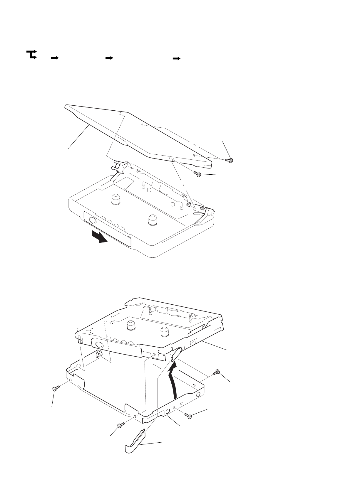
1. Clean the following parts with a denatured-alcohol-moistened
swab :
playback head pinch roller
capstan rubber belt
2. Demagnetize the playback head with a head demagnetizer.
3. Do not use a magnetized screwdriver for the adjustments.
4. After the adjustments, apply suitable locking compound to the
parts adjusted.
5. The adjustments should be performed with the rated power
supply voltage (1.3 V) unless otherwise noted.
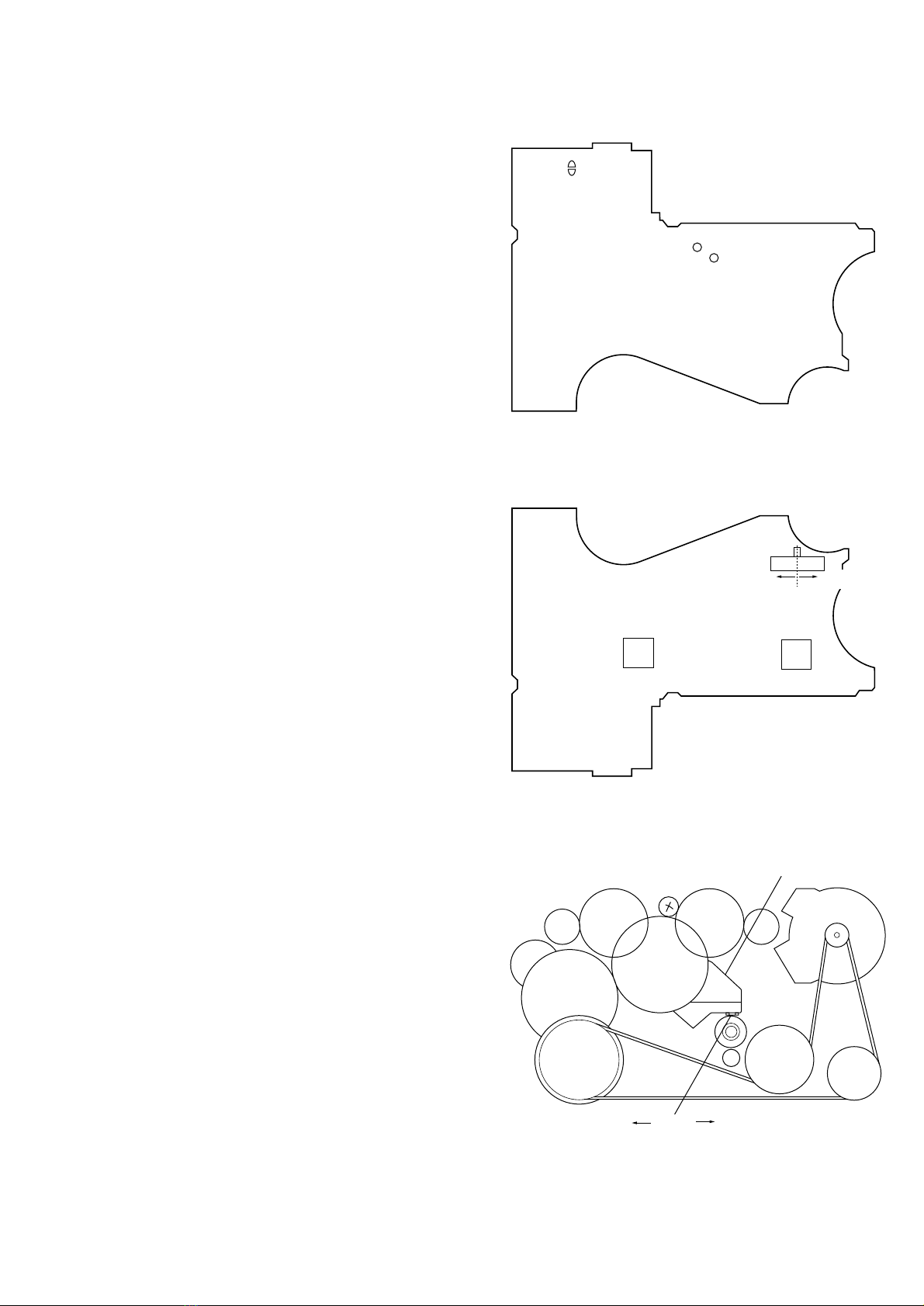
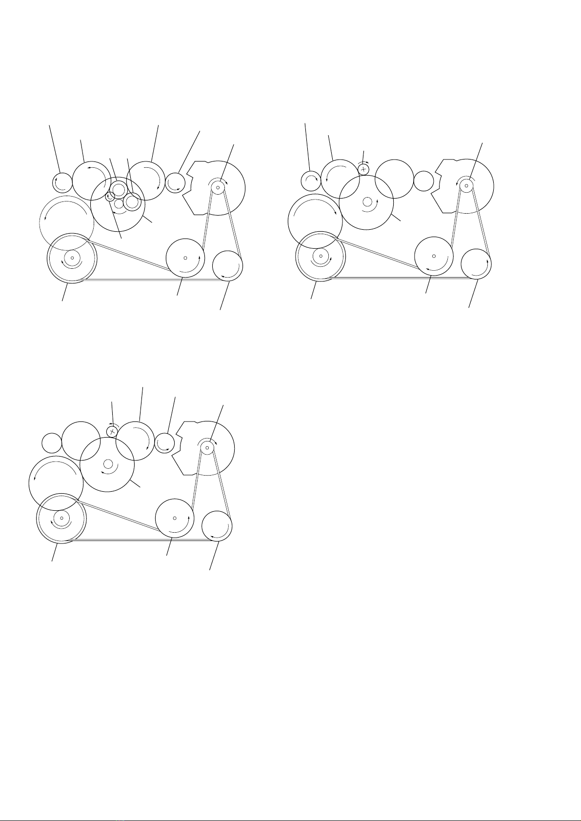
Torque Measurement
Mode Torque Meter Meter Reading
15 – 25 g • cm
FWD CQ-102C (0.21 – 0.35 oz • inch)
FWD less than 2 g • cm
back tension (less than 0.03 oz • inch)
15 – 25 g • cm
REV CQ-102RC (0.21 – 0.35 oz • inch)
REV less than 2 g • cm
back tension (less than 0.03 oz • inch)
more than 50 g • cm
FF, REW CQ-201B (more than 0.69 oz • inch)
SECTION 5
ELECTRICAL ADJUSTMENTS
SECTION 4
MECHANICAL ADJUSTMENTS
PRECAUTION
•Supplied voltage : 1.3 V
•Switches and control position
VOL switch : NORM
•Remote control position
HOLD switch : OFF
VOL control : MAX
SOUND mode : NORM
DOLBY mode : OFF
TestTape
Type Signal Used for
WS-48A 3 kHz, 0 dB tape speed adjustment
Tape Speed Adjustment
Procedure :
1. Playback WS-48A (tape center part) in the REV state and
adjust RV601 so that the digital frequency counter reading
becomes3,000 Hz.
Specification Value :
Digital frequency counter
2,985 to 3,015 Hz
2. Playback WS-48A (tape center part) in the FWD state.
Check that digital frequency counter reading is within 2.5% of
reading of step 1.
Adjustment Location :
RV601
SECTION 6
DIAGRAMS
6-1. IC PIN DESCRIPTION
• IC701 ML63514-017 (SYSTEM CONTROL)
Pin No. Pin Name I/O Pin Description
1 A/B SW I SideA/B detection switch signal input. L: side A, H: side B
2 FWD SW I MD mode switch (FWD) signal input. L: ON
3 CEN SW I MD mode switch (CENTER) signal input. L: ON
4 RVS SW I MD mode switch (RVS) signal input. L: ON
5 CASSETTE SW I Cassette with/without detection switch signal input. L: with, H: without
6 DATA/RMUM I/O Communication data signal output, Remote control with/without detection signal input.
7 REVIVE CTL O Tone select switch signal output. H: REVIVE, L: MEGA BASS/GROOVE
8 MEGA BASS CTL O Tone select switch signal output. H: MEGA BASS, L: OFF/GROOVE
9 F/R CTL O Head select signal output. L: FWD, H: RVS
10 BOOST CTL O Tone select switch signal output. H: BOOST ON, L: OFF
11 AMP CTL O Audio circuit • DDC control signal output. H: POWER ON
12 MUTE CTL O Audio muting control signal output. L: MUTE ON
13 SET STOP1 I Set stop voltage signal input
14 SET STOP2 I Set stop reference voltage signal input
15 BATT DET I Power voltage detection signal input
16 KEY IN I Operation switch signal input
17 PM CTL O Plunger control signal output. L: ON
18 PHOTO (T) CTL O Rotational detection intermittent signal output. (Take-up side) L: ON
19 PHOTO (S) CTL O Rotational detection intermittent signal output. (Supply side) L: ON
20 DOLBY CTL O Dolby circuit control signal output. L: ON
21 VDD1 — Power supply pin. (for external interface)
22 VSS — Ground
23 VDD — Power supply pin
24 VDDH — Backup increased voltage power supply pin
25 CB1 — Increased power supply capacitor connection pin
26 CB2 — Increased power supply capacitor connection pin
27 VDDL — Internal logic positive side power supply pin
28 XT0 I Crystal oscillator connection pin. (32.768 kHz)
29 XT1 O Crystal oscillator connection pin. (32.768 kHz)
30 TEST1B I Test input pin. (Connect to power supply pin.)
31 TEST2B I Test input pin. (Connect to power supply pin.)
32 OSCM — Not used. (Open)
33 OSC0 I High speed CR oscillation (800 kHz) resistor connection pin
34 OSC1 O High speed CR oscillation (800 kHz) resistor connection pin
35 RESET I Reset signal input
36 BEEP O Beep signal output
37 PHOTO (S) IN I Rotational detection signal input
38 PHOTO (T) IN I Rotational detection signal input
39 AMS IN I Music with/without detection (AMS) signal input. (External interruption) H: without
40 P SIG I Motor P-SIG signal input. (External interruption)
41 MOTOR START O Motor wake-up signal output. L: wake-up
42 MOTOR DIR O Motor rotational direction control signal output. H: CCW, L: CW
43 CLRL 2 O Mode select signal output to Motor servo IC (IC601).
44 CLRL 1 O Mode select signal output to Motor servo IC (IC601).
45 MOTOR W O Motor control signal output
46 MOTOR V O Motor control signal output
47 MOTOR U O Motor control signal output
48 1/2 O Motor speed 1/2 control signal output. L: 1/2 high speed, H: normally

– 11 – – 12 –
WM-EX9
6-2. BLOCK DIAGRAM
AMS IN
BEEP
BOOST CTL
F/R CTL
DOLBY CTL
MEGA BASS CTL
REVIVE CTL
XTO
XTI
CASSETE SW
MUTE CTL
PHOTO (T) CTL
PHOTO (T) IN
39
36
20
8
7
10
9
28
29
5
12
18
38
PHOTO (S) IN
37
PHOTO (S) CTL
19
1/2
48
MOTOR START
41
MOTOR U
47
MOTOR V
46
MOTOR W
45
CTRL 1
44
CTRL 2
43
MOTOR DIR
42
P SIG
40
X701
32.768kHz
M/N
CONTROL
Q703
PRE OUT
CONTROL
Q102 PRE OUT
CONTROL
Q202
DOLBY
REG
Q305
MB & RV
CONTROL
Q303
PLUNGER
DRIVER
Q701
RESET
IC704
REVIVE
CONTROL
Q302
RIPPLE
FILTER
VOL MAX
SW
Q103,203
VOL MIN
SW
Q104,204
RIPPLE
FILTER
Q301
METAL
SW
Q101,201
EQ AMP CTL
FOR METAL
Q306
T REEL
SENS
PH702
MOTOR
SW
Q601
-1
(TAPE IN)
-2
(ATS)
15
19
10
41 39 4042434446
S REEL
SENS
PH701
1/2 SPEED
SW
Q604
MOTOR
START SW
Q602
Q702 (1/2)
Q702 (2/2)
RV601
TAPE
SPEED
21
30
29
28
S704
16
17
15
1
36
35 4
5
6
7
8
9
10
31
32
34
19
2
MOTOR SERVO
IC601
9
11
13
2
4
6
8
10
12
1
3
5
MOTOR
SW
Q603
1168
1
2
SWITCH
SWITCH
BEEP
M/N
F/R
BST
PW
MT
AMS DET
VCC
PRE OUT R
PRE OUT L
+
–
+
–
7
5
4
3
AUDIO AMP
IC301 (1/2)
VREF
FWD L
FWD R
REV L
REV R
L
R
L
R
REF V
ICI1
VI1
VI2
IV
U IN
V IN
W IN
CTRL 1
CTRL 2
DIR
PSIG
UT
VT
WT
UT
VT
WT
WS
VS
US
TU
TW
TV
TU
TW
TV
W
V
U
W
V
U
C
04
WS
VS
US
W OUT
V OUT
U OUT
MCENTER
MC
B+
(+1.5V)
SYSTEM
CONTROL
IC701
DATA/PMUM 6
PM CTL 17
RESET 35
A/B SW 1
FWD SW 2
CEN SW 3
RVS SW 4
KEY IN 16
BATT DET 15
AMP CTL 11
B+
(+1.5V)
VREF
11
4
10
14
5
DOLBY AMP
IC302
VCC B+
(+2.5V)
B+
(+2.5V)
S301
VOL
AVLS
MIN
NORM
MAX
PW IN C
PW IN R
PW IN L
PW NF R
PW NF L
29
26
32
27
28
21
35
22
20
+
–
+
–
PW OUT L
PW OUT R
18
17
BASE
RF OUT
PW OUT C
AGC IN
AUDIO AMP
IC301 (2/2)
PM701
PLUNGER
B+ (+1.5V)
S701
(N/R)
FWD
CENTER
RVS
S702
(A/B)
S703
HOLD
1
2
3
4
7
8
OUT1
OUT2
OUT3
OUT4
CE
VCC
VOLTAGE DETECT
IC702
CE LX
V OUT
B+
(+1.5V)
1 5
2
DC/DC CONVERTER
IC703
B+
(+1.5V)
B+
(+2.5V)
RECHAGEABLE
BATTERY
NH-14WM
1.2V 1400mAh
DC IN 1.5V
BATTERY CASE
DRY BATTERY
SIDE "AA"
(IEC DESIGNATION R6)
1PC, 1.5V
GND
REMO
DATA
VCC
J301
REMOTE
CAPSTAN
/REEL
MOTOR
M701
HP701
(PLAYBACK)
L CH
R CH
FWD
L CH
R CH
REV
VREF
• Signal path
: PB

– 13 – – 14 – – 15 –
WM-EX9
6-3. PRINTED WIRING BOARDS (Board suffix No. : -11)
(D101) C-2
(D201) C-2
(D301) C-1
D701 G-14
D702 C-17
D703 B-19
IC301 F-18
IC302 D-18
IC601 D-13
IC701 D-16
IC702 B-17
IC703 G-14
IC704 D-16
PH701 D-13
PH702 D-15
Q101 H-19
Q102 D-19
Q103 D-19
Q104 D-19
Q201 H-19
Q202 D-19
Q203 D-19
Q204 E-19
Q301 G-19
Q302 E-19
Q303 E-19
Q305 E-18
(Q306) F-2
Q601 D-12
Q602 C-14
Q603 F-13
(Q604) D-8
Q701 B-18
Q702 D-15
Q703 E-17
Ref. No. Location
• Semiconductor
Location
( ) : SIDE B
Note:
•r: Through hole.
•b: Pattern from the side which enables seeing.
(The other layer’s patterns are not indicated.)
Caution:
Pattern face side: Partson thepattern facesideseenfromthe
(Side B) pattern face are indicated.
Parts face side: Parts on the parts face side seen from the
(Side A) parts face are indicated.

– 16 – – 17 – – 18 –
WM-EX9
6-4. PRINTED WIRING BOARDS (Board suffix No. : -12)
(D101) C-2
(D201) C-2
(D301) C-1
D701 G-14
D702 C-17
D703 B-19
IC301 F-18
IC302 D-18
IC601 D-13
IC701 D-16
IC702 B-17
IC703 G-14
IC704 D-16
PH701 D-13
PH702 D-15
Q101 H-19
Q102 D-19
Q103 D-19
Q104 D-19
Q201 H-19
Q202 D-19
Q203 D-19
Q204 E-19
Q301 G-19
Q302 E-19
Q303 E-19
Q305 E-18
(Q306) F-2
Q601 D-12
Q602 C-14
Q603 F-13
(Q604) D-8
Q701 B-18
Q702 D-15
Q703 E-17
Ref. No. Location
• Semiconductor
Location
( ) : SIDE B
Note:
•r: Through hole.
•b: Pattern from the side which enables seeing.
(The other layer’s patterns are not indicated.)
Caution:
Pattern face side: Partson thepattern facesideseenfromthe
(Side B) pattern face are indicated.
Parts face side: Parts on the parts face side seen from the
(Side A) parts face are indicated.
• Abbreviation
FR : French model.

– 19 – – 20 – – 21 –
WM-EX9
6-5. SCHEMATIC DIAGRAM • Refer to page 22 for IC Block Diagrams.
Note:
• All capacitors are in µF unless otherwise noted. pF: µµF
50 WV or less are not indicated except for electrolytics
and tantalums.
• All resistors are in Ωand 1/4W or less unless otherwise
specified.
• % : indicates tolerance.
•C: panel designation.
•U: B+ Line.
•H: adjustment for repair.
• Total current is measured with no cassette installed.
• Powervoltageis dc 1.5Vand fed withregulateddc power
supply from battery terminal.
• Voltages is dc with respect to ground in playback mode.
no mark : PB (DOLBY : ON)
∗: Impossible to measure
• Voltagesare takenwith aVOM (Input impedance 10 MΩ).
Voltage variations may be noted due to normal produc-
tion tolerances.
• Signal path.
E: PB
• Abbreviation
FR : French model.

– 22 – – 23 – – 24 –
• IC Block Diagrams
IC301 TA2123F
IC302 NJM2185AV
IC703 XC6383C251ML
+
–
+
–
AGC
DET
BST
PWC
PWB
+
–
PWA
+
–
+
–
+
–
+
–
TOMP
RIPPLE
FILTER
MIX
MTL DRV
VREF
PREA
PREB
BEEP
SW
36 35 34 33 32 31 30 29 28 27 26 25
24
22
21
20
19
18
17
16
15
14
13
23
12111098765321 4
48
47
46
45
44
43
42
41
40
39
38
37
AGC DET
AGC IN
BST NF
BST OUT
PW IN C
LPF
EQ L
PW NF L
PW IN L
PW IN R
PW NF R
EQ R
RF IN
PW GND
PW OUT R
PW OUT C
PW OUT L
VCC
BASE
RF OUT
GND
AMS DET
AMS MIX
AMS IN
VREF IN
PRE GND
M/N SW
PRE SW
F/R SW
BST SW
PW SW
NT SW
AMS OUT
BEEP
MT TC
CAMP SW
AMS IN
PRE NF-R
PRE OUT-R
MTL DRV-R
MTL DRV-L
PRE OUT-L
PRE NF-L
REV IN-L
REV IN-R
REF OUT
FWD IN-R
FWD IN-L
+
–
+
–
BIAS
CIRCUIT
WEIGHT
G2 G1 V/I
ACH BLOCK
GM
SUN
BCH BLOCK (SAME ACH)
14 13 12 11 10 9 8
1 2 3 4 5 6 7
GND I
REF
V
REF
INB OUT B DC B DET B
Vcc SW V
EXT
IN A OUT A DC A DET A
+
–
+
–
CHIP ENABLE
V REF
VDD
2 STEP PFM CONTROL
OSC 100/180 kHz
VLx LIMITER
BUFFER
1
2
3 4
5
CE
V OUT
NC
LX
VSS
IC601 LB1994M
IC702 MM1305 IC704 S-80808ANNP-E7Y
DECODER
CTRL
BLOCK
POWER
D/DT PULSE
BUFFER
COMPARATORBUFFERVI
COMPARATOR
SOFT CLIP
CURRENT
AMP
P-SIG
PW•SW
4 5 61 2 97 8
14
15
16
17
18
19
20212224 23252627
30
29
28
36
35
34
33
32
31
WS MC
U IN
3
VCC
V IN
W IN
CTRL1
CTRL2
DIR
VS
US
U OUT
NC
V OUT
W OUT
WT
VT
UT
PGND
FC
CT2
CT1
IR
ICI2
ICI1
I SOFT
M CENTER
GND
VI2
VI1
IV
VC
13 PW
12 CI
11 Vref
10 P SIG
+
–
+
–
+
–
+
–
1
2
3
4
8
7
6
5
VCC
CE
RIPPLE
GND
OUT 1
OUT 2
OUT 3
OUT 4
+
–
Vref
43
12
VSS NC
OUT VDD
Ref. No. Part No. Description RemarkRef. No. Part No. Description Remark
SECTION 7
EXPLODED VIEWS
NOTE:
• The mechanical parts with no reference
number in the exploded views are not supplied.
• Items marked “*” are not stocked since
they are seldom required for routine service.
Some delay should be anticipated
when ordering these items.
• Board suffix No.
-11 : suffix No. is -11
-12 : suffix No. is -12
• -XX and -X mean standardized parts, so
they may have some difference from the
original one.
• Color Indication of Appearance Parts
Example :
KNOB, BALANCE (WHITE) ... (RED)
Parts Color Cabinet’s Color
7-1. CASE SECTION
N
N
1 3-029-213-01 TERMINAL PLATE
2 3-345-648-71 SCREW (M1.4), TOOTHED LOCK
3 3-375-114-41 SCREW
4 3-029-210-01 TERMINAL PLATE (MINUS)
5 A-3021-147-A MAIN BOARD, COMPLETE (EXCEPT FR)
5 A-3021-207-A MAIN BOARD, COMPLETE (FR)
6 3-029-923-01 LID (N), BATTERY CASE (GOLD) (EXCEPT US)
6 3-029-923-11 LID (L), BATTERY CASE (BLUE) (US,JE)
6 3-029-923-21 LID (B), BATTERY CASE (BLACK) (KR,JE)
7 3-366-892-11 SCREW (M1.4X1.4)
8 X-3376-278-1 TERMINAL PLATE ASSY, BATTERY
9 A-3050-802-A ORNAMENT (OPEN) BLOCK ASSY
10 3-366-892-01 SCREW (M1.4)
11 X-3376-277-1 BRACKET ASSY
12 4-963-883-51 SCREW (M1.4), PRECISION PAN
*13 1-671-401-11 SUB BOARD (JE) (-11)
*13 1-671-401-12 SUB BOARD (-12)
14 3-029-217-01 LEVER (B), LOCK
15 X-3376-371-1 BRACKET (CASSETTE) ASSY
16 3-365-630-41 SCREW (M1.4)
17 3-029-932-01 ORNAMENT (CASSETTE)
18 X-3376-372-1 LID ASSY (N), CASSETTE (GOLD) (EXCEPT US)
18 X-3376-602-1 LID ASSY (L), CASSETTE (BLUE) (US,JE)
18 X-3376-603-1 LID ASSY (B), CASSETTE (BLACK) (KR,JE)
19 3-704-197-41 SCREW (M1.4X2.2), LOCKING (GOLD,BLUE)
19 3-704-197-42 SCREW (M1.4X2.2), LOCKING (BLACK)
20 3-029-205-01 MD COVER (JE)
20 3-029-205-11 MD COVER (EXCEPT JE)
21 3-029-922-01 ORNAMENT (CASE)
22 3-029-921-01 CASE (N) (GOLD) (EXCEPT US)
22 3-029-921-11 CASE (L) (BLUE) (US,JE)
22 3-029-921-21 CASE (B) (BLACK) (KR,JE)
23 3-704-197-01 SCREW (M1.4X1.6), LOCKING (for GOLD,BLUE)
23 3-704-197-03 SCREW (M1.4X1.6), LOCKING (for BLACK)
(KR,JE)
24 3-029-933-01 KNOB (VOL) (N) (GOLD) (EXCEPT US)
24 3-029-933-11 KNOB (VOL) (L) (BLUE) (US,JE)
24 3-029-933-21 KNOB (VOL) (B) (BLACK) (KR,JE)
S704 1-762-553-11 SWITCH, LEAF (TAPE IN,ATS)
B
B
AA
1
2
3
4
563
8
9
101112
12
13
77
14
15
16 17
17
18
19
19
20
21
19
19 22 23
24
S704 MT-WMEX9-162
• Accessories and packing materials are
given in the last of this parts list.
• Abbreviation
FR : French model
KR : Korea model
JE : Tourist model

– 25 –
7-2. MECHANISM DECK SECTION
(MT-WMEX9-162)
Ref. No. Part No. Description Remark Ref. No. Part No. Description Remark
51 X-3376-293-1 HOLDERASSY
52 X-3376-295-1 PINCHLEVER(R)ASSY
53 X-3376-294-1 PINCHLEVER(N)ASSY
54 3-029-275-01 WASHER(ST OPPERN)
55 3-029-278-01 WASHER
56 X-3376-291-1 CHASSISASSY(F)
57 3-386-694-01 WASHER
58 3-029-287-01 SPRING(TG),TORSION
59 3-029-281-01 GEAR,IDLER(B)
60 3-029-306-01 FLYWHEEL(N), INSER T
61 3-029-285-01 GEAR,CAM
62 3-029-282-01 GEAR(Y)
63 3-029-284-01 LEVER,TRIGGER
64 X-3376-813-1 CLUTCHASSY(F)
65 3-932-724-21 WASHER
66 3-029-286-01 GEAR(NR)
67 3-029-884-01 BEL T(F1)
68 3-007-433-01 SHEET(N),REFLECTION
69 3-029-283-01 GEAR,IDLER(A)
70 3-029-765-01 SCREW(M1.4),TOOTHEDLOCK
71 3-029-268-01 FLYWHEEL(R), INSER T
72 3-029-883-01 RET AINERB ASE(F1), MO TOR
73 3-029-273-01 GEAR(FR)
74 3-010-273-02 GEAR(REEL)
75 3-029-288-01 PULLEY ,REVERSE
76 3-010-954-01 SPRING(BT),COMPRESSION
77 3-010-274-02 TABLE, REEL
78 3-029-289-01 WASHER
79 3-029-276-01 WASHER(ST OPPERR)
80 3-007-428-01 WASHER(R)
81 3-029-271-01 SPRING(HD)
HP701 1-500-576-11 HEAD ,MA GNETIC(PLA YB ACK)
M701 1-763-165-11 MOTOR(F1)(CAPST AN/REEL)(includingPULLEY)
PM701 1-454-674-31 SOLENOID,PLUNGER
51
M701
HP701
PM701
52
54
55
53
56
58
59
60 61
62 64
63
65 66
67
68
69 70
71
72
73
74
75
76
77
78
79
81
57
80

– 26 –
SECTION 8
ELECTRICAL PARTS LIST
Ref. No. Part No. Description Remark Ref. No. Part No. Description Remark
MAIN
A-3021-147-A MAINBOARD,COMPLETE(EXCEPTFR)
A-3021-207-A MAINBOARD,COMPLETE(FR)
*********************
<CAP ACIT OR>
C101 1-107-520-11 TANT AL. CHIP 33uF 20% 2.5V
C102 1-164-227-11 CERAMICCHIP 0.022uF 10% 25V
C103 1-115-156-11 CERAMICCHIP 1uF 10V
C105 1-115-156-11 CERAMICCHIP 1uF 10V
C106 1-115-156-11 CERAMICCHIP 1uF 10V
C107 1-113-619-11 CERAMICCHIP 0.47uF 10% 6.3V
C108 1-115-467-11 CERAMICCHIP 0.22uF 10% 10V
C109 1-115-156-11 CERAMICCHIP 1uF 10V
C201 1-107-520-11 TANT AL. CHIP 33uF 20% 2.5V
C202 1-164-227-11 CERAMICCHIP 0.022uF 10% 25V
C203 1-115-156-11 CERAMICCHIP 1uF 10V
C205 1-115-156-11 CERAMICCHIP 1uF 10V
C206 1-115-156-11 CERAMICCHIP 1uF 10V
C207 1-113-619-11 CERAMICCHIP 0.47uF 10% 6.3V
C208 1-115-467-11 CERAMICCHIP 0.22uF 10% 10V
C209 1-115-156-11 CERAMICCHIP 1uF 10V
C301 1-135-316-11 TANT AL. CHIP 22uF 20% 2.5V
C302 1-164-360-11 CERAMICCHIP 0.1uF 16V
C303 1-164-227-11 CERAMICCHIP 0.022uF 10% 25V
C304 1-135-151-21 TANT ALUMCHIP 4.7uF 20% 4V
C305 1-104-847-11 TANT AL. CHIP 22uF 20% 4V
C306 1-125-976-11 TANT AL. CHIP 150uF 20% 2.5V
C307 1-135-151-21 TANT ALUMCHIP 4.7uF 20% 4V
C308 1-165-128-11 CERAMICCHIP 0.22uF 16V
C309 1-165-112-11 CERAMICCHIP 0.33uF 16V
C310 1-115-467-11 CERAMICCHIP 0.22uF 10% 10V
C311 1-135-149-21 TANT ALUMCHIP 2.2uF 20% 10V
C312 1-164-360-11 CERAMICCHIP 0.1uF 16V
C313 1-115-156-11 CERAMICCHIP 1uF 10V
C314 1-125-837-11 CERAMICCHIP 1uF 10% 6.3V
C315 1-164-505-11 CERAMICCHIP 2.2uF 16V
C316 1-135-151-21 TANT ALUMCHIP 4.7uF 20% 4V
C317 1-113-600-11 TANT AL. CHIP 2.2uF 20% 6.3V
C318 1-162-964-11 CERAMICCHIP 0.001uF 10% 50V
C319 1-135-201-11 TANT ALUMCHIP 10uF 20% 4V
C320 1-115-156-11 CERAMICCHIP 1uF 10V
C321 1-162-926-11 CERAMICCHIP 82PF 5% 50V (-11)
C321 1-162-927-11 CERAMICCHIP 100PF 5% 50V (-12)
C322 1-162-964-11 CERAMICCHIP 0.001uF 10% 50V
C601 1-125-837-11 CERAMICCHIP 1uF 10% 6.3V
C602 1-113-619-11 CERAMICCHIP 0.47uF 10% 6.3V
C603 1-165-176-11 CERAMICCHIP 0.047uF 10% 16V
C604 1-165-176-11 CERAMICCHIP 0.047uF 10% 16V
C605 1-119-663-11 TANT AL. CHIP 47uF 20% 2.5V
C606 1-164-227-11 CERAMICCHIP 0.022uF 10% 25V
C607 1-127-671-11 CERAMICCHIP 0.01uF 5% 50V
C608 1-135-149-21 TANT ALUMCHIP 2.2uF 20% 10V
C609 1-115-156-11 CERAMICCHIP 1uF 10V
C610 1-162-964-11 CERAMICCHIP 0.001uF 10% 50V
C611 1-115-156-11 CERAMICCHIP 1uF 10V
C612 1-115-156-11 CERAMICCHIP 1uF 10V
C701 1-135-259-11 TANT AL. CHIP 10uF 20% 6.3V
C702 1-162-964-11 CERAMICCHIP 0.001uF 10% 50V
C703 1-115-156-11 CERAMICCHIP 1uF 10V
C704 1-162-915-11 CERAMICCHIP 10PF 0.5PF 50V
C705 1-115-156-11 CERAMICCHIP 1uF 10V
C706 1-107-826-11 CERAMICCHIP 0.1uF 10% 16V
C707 1-115-156-11 CERAMICCHIP 1uF 10V
C708 1-115-156-11 CERAMICCHIP 1uF 10V
C709 1-125-837-11 CERAMICCHIP 1uF 10% 6.3V
C710 1-115-156-11 CERAMICCHIP 1uF 10V
CB301 1-127-678-21 CERAMICCHIP 330PF 50V (-11)
CB301 1-127-575-21 CERAMICCHIP 470PF 50V (-12)
CB302 1-127-576-21 CERAMICCHIP 0.022uF 50V
<DIODE>
D101 8-719-422-37 DIODE MA8051
D201 8-719-422-37 DIODE MA8051
D301 8-719-422-37 DIODE MA8051
D701 8-719-049-09 DIODE 1SS367-T3SONY
D702 8-719-404-50 DIODE MA111-TX
D703 8-719-422-37 DIODE MA8051
NOTE:
• Due to standardization, replacements in
the parts list may be different from the
parts specified in the diagrams or the
components used on the set.
• -XX and -X mean standardized parts, so
they may have some difference from the
original one.
• RESISTORS
All resistors are in ohms.
METAL:Metal-film resistor.
METAL OXIDE: Metal oxide-film resistor.
F:nonflammable
• Abbreviation
FR : French model
KR : Korea model
JE : Tourist model
• Items marked “*” are not stocked since
they are seldom required for routine service.
Some delay should be anticipated
when ordering these items.
• SEMICONDUCTORS
In each case, u : µ, for example:
uA.. : µA.. uPA.. : µPA..
uPB.. : µPB.. uPC.. : µPC.. uPD.. : µPD..
• CAPACITORS
uF : µF
• COILS
uH : µH
• Board suffix No.
-11 : suffix No. is -11
-12 : suffix No. is -12
The components identified by
mark !or dotted line with mark.
!are critical for safety.
Replace only with part number
specified.
Les composants identifiés par une
marque !sont critiques pour
la sécurité.
Ne les remplacer que par une piéce
portant le numéro spécifié.
When indicating parts by reference
number, please include the board.

– 27 –
Ref. No. Part No. Description Remark Ref. No. Part No. Description Remark
MAIN
<FUSE>
F701 1-533-792-11 FUSE(SMD)(0.25A)
<FERRITEBEAD>
FB701 1-414-760-21 INDUCTOR,FERRITEBEAD
<IC>
IC301 8-759-549-78 IC TA2123F(EL)
IC302 8-759-488-80 IC NJM2185A V-TE2
IC601 8-759-553-51 IC LB1994M-TLM
IC701 8-759-580-18 IC ML63514-017TBZ060
IC702 8-759-438-27 IC MM1305BWBE
IC703 8-759-553-28 IC XC6383C251ML
IC704 8-759-572-21 IC S-80808ANNP-E7Y-T2
<JACK>
J301 1-779-867-81 JACK( 2REMOTE)
<JUMPERRESISTOR>
JC101 1-216-864-11 METALCHIP 0 5% 1/16W
(EXCEPTFR)
JC201 1-216-864-11 METALCHIP 0 5% 1/16W
(EXCEPTFR)
<COIL>
L701 1-412-034-11 INDUCTORCHIP 330uH
<PHOTOREFLECTOR>
PH701 8-749-014-43 PHOTOREFLECTOR PR-20-T
PH702 8-749-014-43 PHOTOREFLECTOR PR-20-T
<TRANSISTOR>
Q101 8-729-028-26 FET 2SK1829(TE85L)
Q102 8-729-028-26 FET 2SK1829(TE85L)
Q103 8-729-028-26 FET 2SK1829(TE85L)
Q104 8-729-230-63 TRANSISTOR 2SC4116-YG
Q201 8-729-028-26 FET 2SK1829(TE85L)
Q202 8-729-028-26 FET 2SK1829(TE85L)
Q203 8-729-028-26 FET 2SK1829(TE85L)
Q204 8-729-230-63 TRANSISTOR 2SC4116-YG
Q301 8-729-800-71 TRANSISTOR 2SB815B7-TB
Q302 8-729-426-36 TRANSISTOR XP1215-TXE
Q303 8-729-426-36 TRANSISTOR XP1215-TXE
Q305 8-729-046-89 TRANSISTOR 2SB970-S(TX).SO
Q306 8-729-037-63 TRANSISTOR UN9115J-(TX).SO
Q601 8-729-043-94 TRANSISTOR CPH3106-PM-TL
Q602 8-729-420-24 TRANSISTOR 2SB1218A-QRS
Q603 8-729-039-36 TRANSISTOR MDC06TR
Q604 8-729-037-76 TRANSISTOR UN9215J-(TX).SO
Q701 8-729-046-89 TRANSISTOR 2SB970-S(TX).SO
Q702 8-729-427-51 TRANSISTOR XP4215-TXE
Q703 8-729-425-46 TRANSISTOR XP4315-TXE
<RESISTOR>
R101 1-216-833-11 METALCHIP 10K 5% 1/16W
(-11)
R101 1-216-831-11 METALCHIP 6.8K 5% 1/16W
(-12)
R102 1-216-837-11 METALCHIP 22K 5% 1/16W
R103 1-216-789-11 METALCHIP 2.2 5% 1/16W
R104 1-216-827-11 METALCHIP 3.3K 5% 1/16W
R105 1-216-839-11 METALCHIP 33K 5% 1/16W
R106 1-216-841-11 METALCHIP 47K 5% 1/16W
R107 1-216-857-11 METALCHIP 1M 5% 1/16W
R108 1-216-824-11 METALCHIP 1.8K 5% 1/16W
(-11)
R108 1-216-823-11 METALCHIP 1.5K 5% 1/16W
(-12)
R109 1-216-821-11 METALCHIP 1K 5% 1/16W
R110 1-216-811-11 METALCHIP 150 5% 1/16W
R111 1-216-845-11 METALCHIP 100K 5% 1/16W
R112 1-216-832-11 METALCHIP 8.2K 5% 1/16W
(-11)
R112 1-216-831-11 METALCHIP 6.8K 5% 1/16W
(-12)
R113 1-216-834-11 METALCHIP 12K 5% 1/16W
(-11)
R113 1-216-835-11 METALCHIP 15K 5% 1/16W
(-12)
R150 1-216-813-11 METALCHIP 220 5% 1/16W
(FR:-12)
R201 1-216-833-11 METALCHIP 10K 5% 1/16W
(-11)
R201 1-216-831-11 METALCHIP 6.8K 5% 1/16W
(-12)
R202 1-216-837-11 METALCHIP 22K 5% 1/16W
R203 1-216-789-11 METALCHIP 2.2 5% 1/16W
R204 1-216-827-11 METALCHIP 3.3K 5% 1/16W
R205 1-216-839-11 METALCHIP 33K 5% 1/16W
R206 1-216-841-11 METALCHIP 47K 5% 1/16W
R207 1-216-857-11 METALCHIP 1M 5% 1/16W
R208 1-216-824-11 METALCHIP 1.8K 5% 1/16W
(-11)
R208 1-216-823-11 METALCHIP 1.5K 5% 1/16W
(-12)
R209 1-216-821-11 METALCHIP 1K 5% 1/16W
R210 1-216-811-11 METALCHIP 150 5% 1/16W
R211 1-216-845-11 METALCHIP 100K 5% 1/16W
R212 1-216-832-11 METALCHIP 8.2K 5% 1/16W
(-11)
R212 1-216-831-11 METALCHIP 6.8K 5% 1/16W
(-12)
R213 1-216-834-11 METALCHIP 12K 5% 1/16W
(-11)
R213 1-216-835-11 METALCHIP 15K 5% 1/16W
(-12)

– 28 –
Ref. No. Part No. Description Remark
MAIN
R250 1-216-813-11 MET ALCHIP 220 5% 1/16W
(FR:-12)
R301 1-216-851-11 MET ALCHIP 330K 5% 1/16W
R302 1-216-829-11 MET ALCHIP 4.7K 5% 1/16W
R303 1-216-839-11 MET ALCHIP 33K 5% 1/16W
R304 1-216-837-11 MET ALCHIP 22K 5% 1/16W
R305 1-216-793-11 RES,CHIP 4.7 5% 1/16W
R306 1-216-823-11 MET ALCHIP 1.5K 5% 1/16W
R307 1-216-849-11 MET ALCHIP 220K 5% 1/16W
R308 1-218-884-11 RES,CHIP 36K 0.50% 1/16W
(-11)
R308 1-218-887-11 RES,CHIP 47K 0.50% 1/16W
(-12)
R309 1-216-837-11 MET ALCHIP 22K 5% 1/16W
R310 1-216-853-11 MET ALCHIP 470K 5% 1/16W
R311 1-216-853-11 MET ALCHIP 470K 5% 1/16W
R312 1-216-853-11 MET ALCHIP 470K 5% 1/16W
R314 1-216-841-11 MET ALCHIP 47K 5% 1/16W
R315 1-216-809-11 MET ALCHIP 100 5% 1/16W
R316 1-216-853-11 MET ALCHIP 470K 5% 1/16W
R317 1-218-899-11 RES,CHIP 150K 0.50% 1/16W
(-12)
R601 1-216-845-11 MET ALCHIP 100K 5% 1/16W
R602 1-216-853-11 MET ALCHIP 470K 5% 1/16W
R603 1-216-847-11 MET ALCHIP 150K 5% 1/16W
R604 1-216-845-11 MET ALCHIP 100K 5% 1/16W
R605 1-216-849-11 MET ALCHIP 220K 5% 1/16W
R606 1-216-831-11 MET ALCHIP 6.8K 5% 1/16W
R607 1-216-845-11 MET ALCHIP 100K 5% 1/16W
R608 1-216-851-11 MET ALCHIP 330K 5% 1/16W
R609 1-216-857-11 MET ALCHIP 1M 5% 1/16W
R610 1-216-857-11 MET ALCHIP 1M 5% 1/16W
R611 1-216-845-11 MET ALCHIP 100K 5% 1/16W
R612 1-216-841-11 MET ALCHIP 47K 5% 1/16W
R613 1-216-841-11 MET ALCHIP 47K 5% 1/16W
R614 1-216-837-11 MET ALCHIP 22K 5% 1/16W
R701 1-216-803-11 MET ALCHIP 33 5% 1/16W
R702 1-216-845-11 MET ALCHIP 100K 5% 1/16W
R703 1-216-839-11 MET ALCHIP 33K 5% 1/16W
R704 1-218-447-11 RES,CHIP 62K 5% 1/16W
(-11)
R704 1-216-843-11 MET ALCHIP 68K 5% 1/16W
(-12)
R705 1-216-849-11 MET ALCHIP 220K 5% 1/16W
R706 1-218-907-11 RES,CHIP 330K 0.50% 1/16W
R707 1-216-821-11 MET ALCHIP 1K 5% 1/16W
R708 1-216-853-11 MET ALCHIP 470K 5% 1/16W
R709 1-216-845-11 MET ALCHIP 100K 5% 1/16W
R710 1-218-907-11 RES,CHIP 330K 0.50% 1/16W
R711 1-218-892-11 RES,CHIP 75K 0.50% 1/16W
(-11)
R711 1-218-899-11 RES,CHIP 150K 0.50% 1/16W
(-12)
R712 1-218-907-11 RES,CHIP 330K 0.50% 1/16W
R713 1-216-853-11 MET ALCHIP 470K 5% 1/16W
R714 1-216-823-11 MET ALCHIP 1.5K 5% 1/16W
SUB
R715 1-216-854-11 METALCHIP 560K 5% 1/16W
(-11)
R715 1-216-855-11 METALCHIP 680K 5% 1/16W
(-12)
R716 1-216-823-11 METALCHIP 1.5K 5% 1/16W
R717 1-216-854-11 METALCHIP 560K 5% 1/16W
(-11)
R717 1-216-855-11 METALCHIP 680K 5% 1/16W
(-12)
R718 1-218-873-11 RES,CHIP 12K 0.50% 1/16W
(-11)
R718 1-218-875-11 RES,CHIP 15K 0.50% 1/16W
(-12)
R719 1-218-903-11 RES,CHIP 220K 0.50% 1/16W
R720 1-218-870-11 RES,CHIP 9.1K 0.50% 1/16W
(-11)
R720 1-218-871-11 RES,CHIP 10K 0.50% 1/16W
(-12)
R721 1-218-836-11 RES,CHIP 360 0.50% 1/16W
(-11)
R721 1-218-839-11 RES,CHIP 470 0.50% 1/16W
(-12)
R722 1-218-895-11 RES,CHIP 100K 0.50% 1/16W
(-12)
R723 1-218-851-11 RES,CHIP 1.5K 0.50% 1/16W
(-12)
R724 1-218-899-11 RES,CHIP 150K 0.50% 1/16W
(-12)
<NETWORKRESISTOR>
RB701 1-234-247-21 RES,NETWORK 470K (3216)
<VARIABLERESIST OR>
RV601 1-223-325-21 RES, ADJ ,MET ALGLAZE 100K
<SWITCH>
S301 1-692-605-11 SWITCH,SLIDE(VOL)
S701 1-771-475-21 SWITCH,SLIDE(N/R)
S702 1-762-516-11 SWITCH,PUSH(1KEY)(A/B)
<VIBRA TOR>
X701 1-579-258-11 VIBRA TOR, CR YST AL(32.768kHz)
*************************************************************
*1-671-401-11 SUBBOARD
**********
<SWITCH>
S703 1-771-053-21 SWITCH,KEYBOARD(HOLD)
*************************************************************
Ref. No. Part No. Description Remark

– 29 –
Ref. No. Part No. Description Remark
MISCELLANEOUS
***************
HP701 1-500-576-11 HEAD ,MAGNETIC(PLA YB ACK)
M701 1-763-165-11 MOTOR(F1)(CAPST AN/REEL)(includingPULLEY)
PM701 1-454-674-32 SOLENOID,PLUNGER
S704 1-762-553-11 SWITCH, LEAF(T APEIN,A TS)
*************************************************************
ACCESSORIES&P ACKINGMA TERIALS
********************************
1-418-020-11 REMOTECONTROLUNIT(RM-WME21L)
!1-528-252-21 BATTER YCHARGER(BC-7S)(UK)
1-528-299-41 BATTER Y,Ni-Cd(NC-6WM)(US,AEP ,UK,FR)
!1-528-580-21 BATTER YCHARGER(BC-7HT)(E,JE)
!1-528-676-22 BATTER YCHARGER(BC-9HR)(KR)
!1-528-713-21 BATTER YCHARGER(BC-7DC)(US)
!1-528-744-23 BATTER YCHARGER(BC-7D Y)(AEP ,FR)
1-528-842-11 BATTER Y,NICKELHYDR OGEN(NH-14WM)
(E,JE,KR)
!1-569-007-11 ADAPTOR,CONVERSION2P(E,JE)
1-759-213-21 CASE, BATTER Y(US,E,JE,KR)
1-759-700-21 CASE, BATTER Y(AEP ,UK,FR)
3-008-521-01 CASE, BATTER YCHARGE(forNC-6WM/NH-14WM)
3-864-894-01 MANU AL, INSTR UCTION(J APANESE,ENGLISH,
KOREAN)(JE)
3-864-894-11 MANUAL,INSTRUCTION(ENGLISH,FRENCH)
(US,AEP ,UK,FR)
3-864-894-21 MANUAL,INSTRUCTION(GERMAN,DUTCH) (AEP)
3-864-894-31 MANU AL, INSTR UCTION(SWEDISH,IT ALIAN)
(AEP)
3-864-894-41 MANU AL, INSTR UCTION(SP ANISH,
POR TUGUESE)(AEP)
3-864-894-51 MANUAL,INSTRUCTION(FINNISH,RUSSIAN) (AEP)
3-864-894-61 MANUAL,INSTRUCTION(ENGLISH,CHINESE,
KOREAN)(E,KR)
3-929-799-01 CASE, CARR YING
8-953-220-90 HEADPHONEMDR-ED132SP//KSET
The components identified by
mark !or dotted line with mark.
!are critical for safety.
Replace only with part number
specified.
Les composants identifiés par une
marque !sont critiques pour la
sécurité.
Nelesremplacer que par une piéce
portant le numéro spécifié.

– 30 –
Sony Corporation
Personal A&V Products Company
9-924-980-12
WM-EX9
99A0486-1
Printed in Japan C1999. 1
Published by Quality Engineering Dept.
(Shibaura)
Other manuals for Walkman WM-EX9
2
Table of contents
Other Sony Cassette Player manuals

Sony
Sony NW-A100TPS User manual

Sony
Sony CF-SW1000T User manual

Sony
Sony CFM-10 Operating Instructions (primary... User manual

Sony
Sony TC-KA2ES User manual

Sony
Sony TCM-27 User manual

Sony
Sony Walkman WM-FX522 User manual

Sony
Sony Pressman TCS-100DV User manual

Sony
Sony Walkman WM-FX195 User manual

Sony
Sony TC-R303 User manual

Sony
Sony CFM-D1 User manual

Sony
Sony CFS-515S User manual

Sony
Sony CFS-E14 User manual

Sony
Sony Walkman WM-F2085 User manual

Sony
Sony Walkman WM-FX288 User manual

Sony
Sony DXA-WZ5 User manual

Sony
Sony TC-PB5 User manual

Sony
Sony TC-WA8ESA User manual

Sony
Sony CFD-S07CP User manual

Sony
Sony WM-FX673 User manual

Sony
Sony TC-WR745S User manual