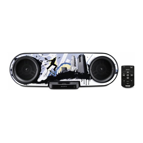
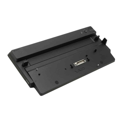
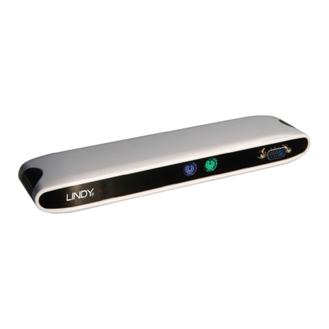
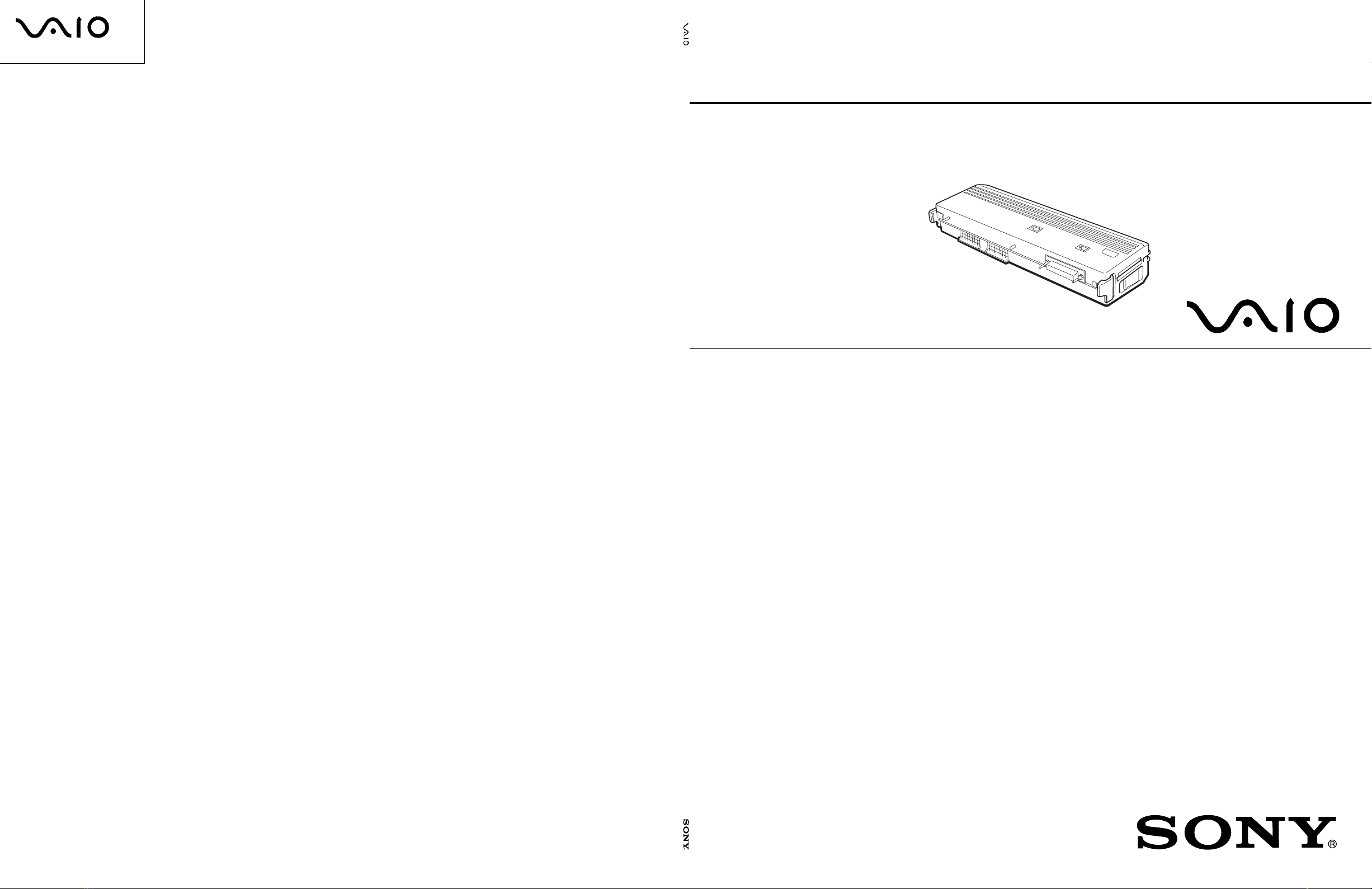
Sony Vaio PCGA-PSX1 User manual

Sony Corporation
Information Technology Company
—XX —
English
99XXXXX-1
Printed in XXXXX
© 1999. X
9-872-034-11 VAIO CUSTOMER LINK (JAPAN)
PCGA-PSX1
9-872-034-11
Power-Up Station
SERVICE MANUAL
PCGA-PSX1 (U/C)
US Model
Canadian Model
PCGA-PSX1 (U/C) 99XXXXX-1
9-872-034-11

— 2 —PCGA-PSX1 (U/C)
Information in this document is subject to change without
notice.
Sony and VAIO are trademarks of Sony. Intel logo and Intel
Inside logo are registered trademarks of Intel Corporation.
Pentium MMX is a trademarks of Intel Corporation. Microsoft,
MS-DOS, Windows, the Windows 95 and Windows 98 logo are
trademarks of Microsoft Corporation.
All other trademarks are trademarks or registered trademarks of
their respective owners. Other trademarks and trade names may
be used in this document to refer to the entitles claiming the
marks and names or their produces. Sony Corporation disclaims
any proprietary interest in trademarks and trade names other than
its own.
1. Obey precautionary markings and
instructions
Labels and stamps on the cabinet, chassis, and components iden-
tify areas requiring special precautions. Be sure to observe these
precautions, as well as all precautions listed in the operating
manual and other associated documents.
2. Use designated parts only
The set’s components possess important safety characteristics,
such as noncombustibility and the ability to tolerate large
voltages. Be sure that replacement parts possess the same safety
characteristics as the originals.Also remember that the ( mark,
which appears in circuit diagrams and parts lists, denotes com-
ponentsthathaveparticularlyimportantsafetyfunctions;beextra
sure to use only the designated components.
3. Always follow the original design
when mounting parts and routing wires
The original layout includes various safety features, such as in-
clusion of insulating materials (tubes and tape) and the mount-
ing of parts above the printer board. In addition, internal wiring
has been routed and clamped so as to keep it away from hot or
high-voltage parts. When mounting parts or routing wires. there-
fore, be sure to duplicate the original layout.
Caution Markings for Lithium/Ion Battery - The following or
similar texts shall be provided on battery pack of equipment or
in both the operating and the service instructions.
CAUTION:Dangerofexplosionifbatteryisincorrectly replaced.
Replace only with the same or equivalent type recommended by
the manufacturer. Discard used batteries according to the manu-
facturer’s instructions.
CAUTION: The battery pack used in this device may present a
fire or chemical burn hazard if mistreated. Do not disassemble,
heat above 100˚C (212˚F) or incinerate.
Dispose of used battery promptly.
Keep away from children.
4. Inspect after completing service
After servicing, inspect to make sure that all screws, compo-
nents, and wiring have been returned to their original condition.
Also check the area around the repair location to ensure that
repair work has caused no damage, and confirm safety.
5. When replacing chip components...
Never reuse components. Also remember that the negative side
of tantalum capacitors is easily damaged by heat.
6. When handling flexible print boards...
• Thetemperatureof the soldering-iron tip should be about 270C.
• Do not apply the tip more than three times to the same pattern.
• Handle patterns with care; never apply force.
Caution: Remember that hard disk drives are easily damaged
by vibration.Always handle with care.
Service and Inspection Precautions
†
†
†
†
†
†
†
†
†
†
†
†
†
†
†
†
†
†
†
†
†
†
†
†
†
†
†
†
†
†
†
†
†
†
— 3 — PCGA-PSX1 (U/C)
TABLE OF CONTENTS
CHAPTER 1. REMOVAL
1-1. Flowchart ................................................................................................... 1-1
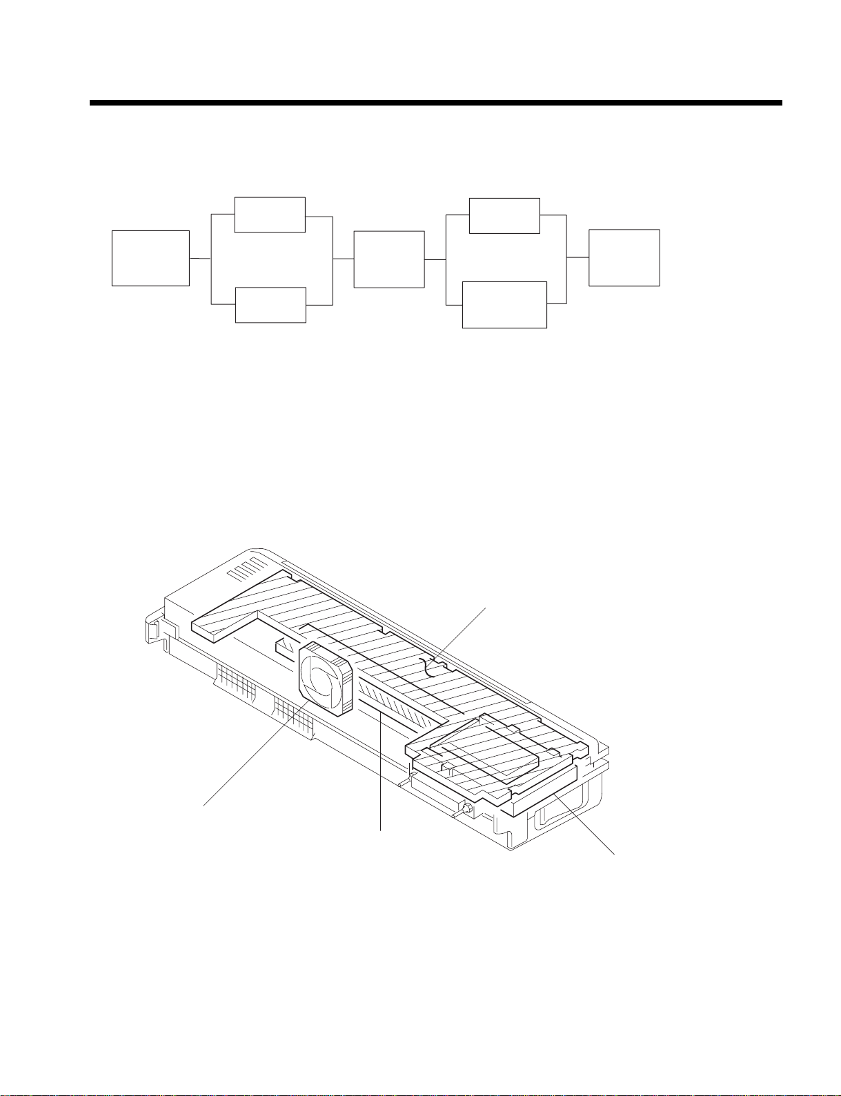
1-2. Electric Parts Arrangement Diagram ......................................................... 1-1
1-3. Removal ..................................................................................................... 1-2
1. DOC CAB BottomAssy ............................................................................ 1-2
2. DC Fan, CNX-70 Board, IFX-67 Board Assy ........................................... 1-3
3. I/O Bracket, Reverse PC Card Connector, IFX-67 Board ......................... 1-4
(to 1-4)
CHAPTER 2. SELF-DIAGNOSIS
2-1. Special Tools and Peripherals to Prepare ................................................... 2-1
2-2. System Connection Diagram for Testing ...................................................2-3
2-3. How to Start Self-Diagnosis ...................................................................... 2-4
(to 2-4)
CHAPTER 3. SEMICONDUCTOR PIN ASSIGNMENTS
Semiconductors Index ............................................................................................. 3-1
Semiconductor Pin Assignments ............................................................................. 3-2
(to 3-10)
CHAPTER 4. DIAGRAMS
4-1. Block Diagram ........................................................................................... 4-1
4-2. Schematic Diagrams and Printed Wired Boards ........................................ 4-2
4-2-1. CNX-70 Board ..................................................................................... 4-2
Parts Location Index............................................................................. 4-2
INDEX ................................................................................................. 4-3
FFC CONNECTOR TO IFX67............................................................ 4-4
SERIAL&PARALLEL CONNECTOR ............................................... 4-5
AUDIO, PS/2 CONNECTOR .............................................................. 4-6
Signal Cross-Reference ........................................................................ 4-7
Unit Cross-Reference ........................................................................... 4-8
Printed Wired Board ............................................................................. 4-9
4-2-2. IFX-67 Board ..................................................................................... 4-10
Parts Location Index........................................................................... 4-10
INDEX ............................................................................................... 4-13
DOCKING CONNECTOR ................................................................ 4-14
PC CARD ........................................................................................... 4-15
AUDIO ............................................................................................... 4-16
CONTROL A1/SERIAL BUFFER .................................................... 4-17
VIDEO CONNECTOR ...................................................................... 4-18
MISC CONNECTORS....................................................................... 4-19
FFC CONNECTOR TO CNX70........................................................ 4-20

— 4 —PCGA-PSX1 (U/C)
Note: The parts location index which precedes
every schematic diagram, serves as the
electrical part list too.
POWER ..............................................................................................4-21
BBCRISIS, EMERGENCY IC ..........................................................4-22
Signal Cross-Reference ......................................................................4-23
Unit Cross-Reference .........................................................................4-24
Printed Wired Board ...........................................................................4-25
(to 4-25)
CHAPTER 5. EXPLODED VIEW AND PARTS LIST..................................5-1
(to 5-1)

1-1 PCGA-PSX1 (U/C)
CHAPTER 1.
REMOVAL
IFX-67 Board
Reverse PC Card
Connector
CNX-70 Board
DC Fan
DOC CAB
BOTTOM
ASSY
P 1-2
DC FAN
CNX-70
BOARD
IFX-67
BOARD
ASSY
I/O
BRACKET
P 1-3
P 1-3
P 1-3
P 1-4
P 1-4
P 1-4
IFX-67
BOARD
REVERSE
PC CARD
CONNECTOR
1-1. Flowchart
• Page x-x indicates the page for the topic.
1-2. Electric Parts Arrangement Diagram

1-2PCGA-PSX1 (U/C)
1. DOC CAB Bottom Assy
1-3. Removal
+P 2.6X8
+B 2X6
(X2) (X6)
+P 2X6
DOC CAB Bottom Assy
(X2)

1-3 PCGA-PSX1 (U/C)
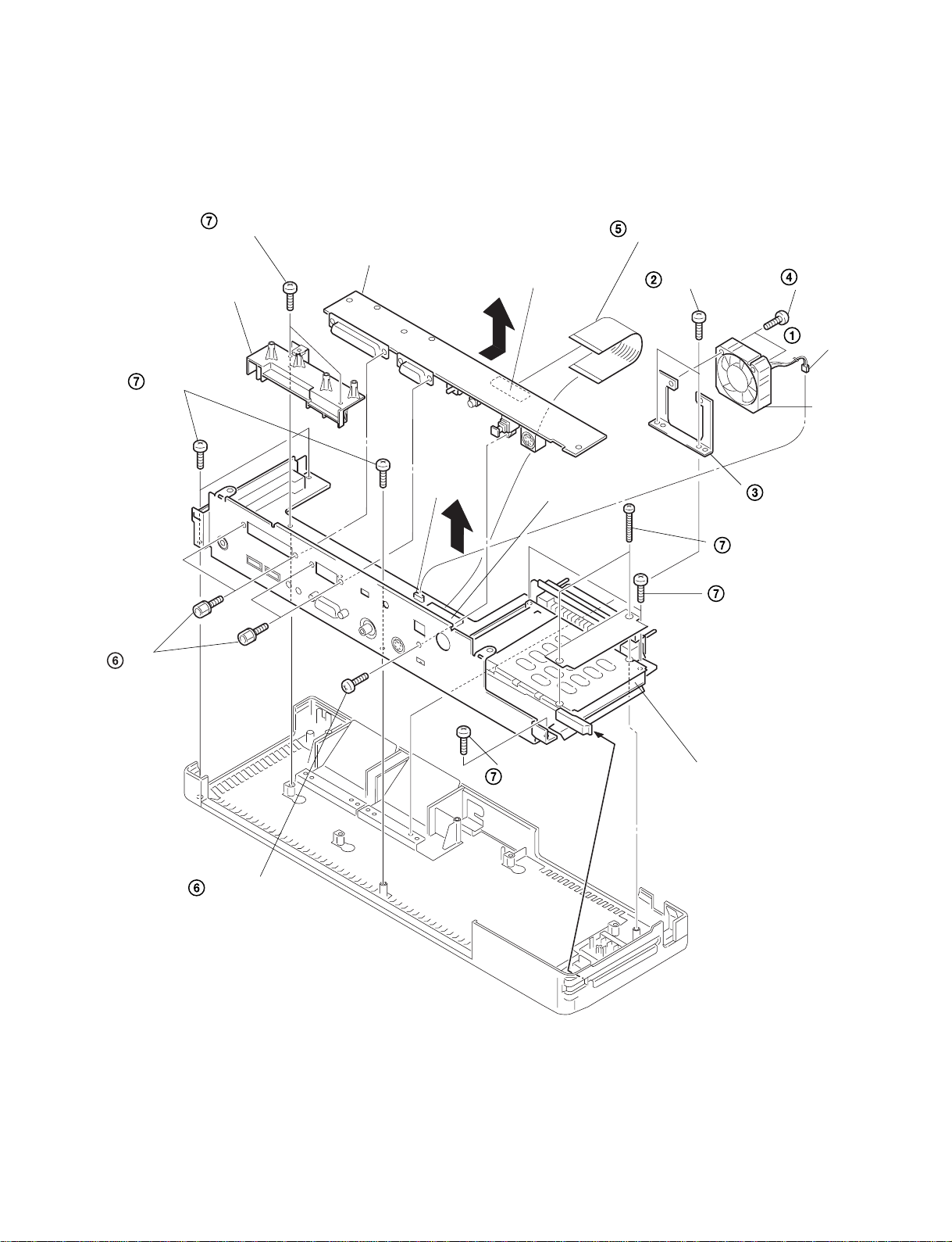
2. DC Fan, CNX-70 Board, IFX-67 Board Assy
Fan Cable
+
+P 2X6 (X2) P M3X16
FFC(Aluminum,Dock)
CNX-70 Board
CN 451
+P 2X6 (X2)
+P 2X6 (X3)
Screw
+BVTP 3X12
+P 2X6
+P 2X6 (X2)
+P M2X19 (X2)
Fan Bracket
CNX-70 Board
IFX-67
Board
CN256
PC Card Fixed
Mold
IFX-67 Board Assy
IFX-67 Board
CN 301
DC Fan
(x2)
(HEX) (X4)

1-4PCGA-PSX1 (U/C) (END)
3. I/O Bracket, Reverse PC Card Connector, IFX-67 Board
Reverse
PC Card Connector
IFX-67 Board
+B 2X14 (X2)
I/O Bracket
Screw
(HEX) (X2)

2-1 PCGA-PSX1 (U/C)
CHAPTER 2.
SELF-DIAGNOSIS
Special tools for serial loopback
Loopback tools designated by QA Plus/Factory
(see next page)
Special tools for parallel loopback
Loopback tools designated by QA Plus/Factory
(see next page)
NTSC monitor (PAL monitor) and a video cable
USB Tester
USB Host Production Tester manufactured by
Computer Access Technology Corporation
PCG-XR series main unit
External floppy-disk drive (FDD) and FDD cable
Diagnostics FD Media
CD-R Bay
Diagnostics CD-ROM Media
AC Adaptor
PS/2 keyboard, PS/2 mouse, and PS/2 yoked-type cable
VGA monitor and monitor cable
MD recorder, such as MDS-PC1
(provided with an optical input and controlA1II terminal)
PCG-XR series for an IEEE1394 test
PC Card Tester
PCCtest450 manufactured by Sycard
1
2
3
4
5
6
7
8
9
10
11
12
13
14
15
Serial port (COM) test
Parallel port (for printer) test
Test for the monitor output (composite) and
S-Video signal
Test for a USB device
(for self-diagnosis)
Test for an FDD
(start-up software for self-diagnosis)
CD-ROM test
(Self-diagnosis program)
(power supply)
PS/2 test
VGA output test
Test for optical output and control A1
IEEE1394 test
Test for PC card slot
Special tools or peripherals Test items
2-1. Special Tools and Peripherals to Prepare

2-2PCGA-PSX1 (U/C)
• Connector Types DB25P(Males)
• Interface Standard Centronics
• Loopback Status to Commands
PARALLEL LOOPBACK CONNECTOR CONNECTION DIAGRAM
1
2
3
4
5
6
7
8
9
10
11
12
13
14
15
16
17
18
19
20
21
22
23
24
25
D0
D1
D2
D3
D4
D5
D6
D7
-ACK
BUSY
PE
SLCT
-STROBE -AUTO FD
-ERROR
-INT
-SLCT IN
GND
GND
GND
GND
GND
GND
GND
GND
DB25P
1
2
3
4
5
6
7
8
9
DB9S
DCD
RX
TX
DTR
GND
DSR
RTS
CTS
RI
• Connector Types DB9S (Females)
• Interface Standard RS-232C
• Loopback Data & Handshake
SERIAL LOOPBACK CONNECTOR CONNECTION DIAGRAM
[Reference] About Special Tools for Serial/Parallel Loopback
• Special tools are needed when self-diagnosis for serial circuits or parallel circuits is to be performed. Prepare special tools as
required, referring to the following connection diagrams.
Serial loopback tools: For testing the serial port
Parallel loopback tools: For testing the parallel port (for the printer)
Note : • Soldering
Note : • Soldering

2-3 PCGA-PSX1 (U/C)
2-2. System Connection Diagram for Testing
PS/2
i.LINK
Mouse
External
FDD
MD deck
Diagnostics
PC card tester
LINE IN
FDD
cable
keyboard
FD media
System Connection Diagram
NTSC/PAL monitor VGA monitor
Mini-plug VGA
out
Parallel Serial
Parallel
output
Parallel
Diagnostics
CD-R bay
Power-Up Station
PCGA-PSX1
USB tester
Serial
output
PCG-XR Series
AC adaptor
Battery
HDD
USB
connector
PCG-XR
loopback tool loopback tool
series
CD-ROM media

2-4PCGA-PSX1 (U/C) (END)
2-3. How to Start Self-Diagnosis
1. Insert the Diagnostics floppy disk into the external floppy-disk drive, and turn on the main unit.
2. When the system starts, the following message is displayed.
Insert PCGA-PSX1 Diagnostics CD-ROM
Insert the Diagnostics CD into the CD-R Bay.
3. The following Top Menu is displayed:
PCGA-PSX1 Diagnostics program Version 1.0
Copyright (c) Sony Corporation 1999. All rights reserved.
Top Menu
1.Execute batch diagnostics
2.Go to sub menu
3.Exit menu
Select menu:
When “1” is selected, the self-diagnosis for the Power-Up station starts.
When “2” is selected, the Submenu is displayed, from which you can select a test to be proceeded.
When “3” is selected, the self-diagnosis program will terminate.

3-1 PCGA-PSX1 (U/C)
IC
TYPE PAGE
INDEX
CHAPTER 3.
SEMICONDUCTOR PIN ASSIGNMENTS
1SS355TE-17 _______________ 3-10
2SC2712-YG-TE85L _________ 3-9
2SK1824-T1 ________________ 3-9
ADM3311EARU-REEL7 ______ 3-2
AK4543VQ _________________ 3-2
EC10QS04-TE12L5 __________ 3-10
GP1F32T ___________________ 3-3
MA3J14300LSO _____________ 3-10
MA8062-H-TX _______________ 3-10
MIC2562A-1BM T&R _________ 3-3
MIC5205BM5T&R ___________ 3-4
NC7SZ125P5X ______________ 3-4
NC7SZ384P5X ______________ 3-4
NDS355AN _________________ 3-9
NM24C02LEM8X ____________ 3-5
NM24C02LEM8X-AO ________ 3-5
R5C475II-LQFP144 __________ 3-5
RB501V-40TE-17 ____________ 3-10
RD36SB-T1 _________________ 3-10
RN5VD16AA-TL _____________ 3-7
RN5VD26AA-TL _____________ 3-7
RN5VD42AA-TL _____________ 3-7
SI6466DQ-T1 _______________ 3-9
SML-310MTT86 _____________ 3-10
SML-311DTT86 _____________ 3-10
SN74CBTD3306PWR ________ 3-7
TC7SET08FU(TE85R) ________ 3-7
TC7SH00FU-TE85R__________ 3-8
TC7SH04FU-TE85R__________ 3-8
TC7SH08FU-TE85R__________ 3-8
UN9210J-(TX).SO ___________ 3-9
UN921DJ-(TX).SO ___________ 3-9
UPA606T-T1 ________________ 3-9
UPD78082GB-A26-3BS-MTX _ 3-8
XN0F256001S0 _____________ 3-9
Semiconductors Index

3-2PCGA-PSX1 (U/C)
IC
ADM3311EARU-REEL7 (ANALOG DEVICES)
RS-232C LINE DRIVER / RECEIVER
– TOP VIEW –
AK4543VQ (AHK)
AUDIO CODEC ’97 REV 2.1
– TOP VIEW –

3-3 PCGA-PSX1 (U/C)
IC
GP1F32T (SHARP)
OPTICAL FIBER LINK TRANSMISSION UNIT
FOR DIGITAL AUDIO INTERFACE
– TOP VIEW –
MIC2562A-1BMT&R (MICREL)
PCMCIA/CARD BUS SOCKETPOWER CONTROLLER
– TOP VIEW –

3-4PCGA-PSX1 (U/C)
IC
MIC5205BM5T&R (MICREL)
150mA LOW-NOISE LDO VOLTAGE REGULATOR
– TOP VIEW –
NC7SZ125P5X (FAIRCHILD)
UHS BUFFER WITH 3-STATE OUTPUT
– TOP VIEW –
NC7SZ384P5X (FAIRCHILD)
UHS 1-BIT LOW POWER BUS SWITCH
– TOP VIEW –

3-5 PCGA-PSX1 (U/C)
IC
NM24C02LEM8X (FAIRCHILD)
NM24C02LEM8X-AO (FAIRCHILD)
2K-BIT SERIAL EEPROM
– TOP VIEW –
R5C475II-LQFP144 (RICOH)
PCI-CARD BUS BRIDGE
– TOP VIEW –

3-6PCGA-PSX1 (U/C)
IC

3-7 PCGA-PSX1 (U/C)
IC
RN5VD16AA-TL (RICOH)
RN5VD26AA-TL (RICOH)
RN5VD42AA-TL (RICOH)
CMOSVOLTAGE DETECTOR
– TOP VIEW –
SN74CBTD3306PWR (TI)
DUALBUS SWITCH WITE LEVEL SHIFTING
–TOP VIEW –
TC7SET08FU (TE85R) (TOSHIBA)
CMOS 2-INPUTAND GATE
– TOP VIEW –

3-8PCGA-PSX1 (U/C)
IC
TC7SH00FU-TE85R (TOSHIBA)
CMOS 2-INPUT NAND GATE
– TOP VIEW –
TC7SH04FU-TE85R (TOSHIBA)
CMOS INVERTER
– TOP VIEW –
TC7SH08FU-TE85R (TOSHIBA)
CMOS 2-INPUTAND GATE
– TOP VIEW –
UPD78082GB-A26-3BS-MTX (NEC)
8-BIT SINGLECHIP MICROCOMPUTER
– TOP VIEW –
Table of contents
Other Sony Docking Station manuals

Sony
Sony RDP-M7IP User manual

Sony
Sony RDP-X30IP User guide

Sony
Sony RDP-XF100IP User manual

Sony
Sony DK52 User manual

Sony
Sony Dream Machine ICF-DS15IP User manual

Sony
Sony RDP-M15IP User guide

Sony
Sony RDP-X200IP Guide

Sony
Sony RDP-X60iP User manual

Sony
Sony RDP-X30iP User manual

Sony
Sony RDP-M15iP User manual

Sony
Sony CSS-HD1 Manual de instrucciones / Manual de... Setup guide

Sony
Sony RDP-M7iP User manual

Sony
Sony RDP-M5iP User manual

Sony
Sony Dream Machine ICF-DS15IP User manual

Sony
Sony NWZ-X1050 User manual

Sony
Sony RDO-X500iP User manual

Sony
Sony TDM-iP50 - Digital Media Port Cradle User manual

Sony
Sony XDR-DS16IP User guide

Sony
Sony RDP-XA700iP User manual

Sony
Sony RDP-V20iP User manual