Sony MDR-RF845R User manual

MDR-RF845R
AEP Model
UK Model
SERVICE MANUAL
HEADPHONES
Sony Corporation
Personal Audio Company
Published by Sony Engineering Corporation
9-927-958-12
2001K1600-1
© 2001.11
Ver 1.2 2001. 11
Headphones MDR-RF845R
Transmitter TMR-RF845R
MDR-RF845R is the component model block one in the MDR-RF845RK.
COMPONENT MODEL NAME FOR MDR-RF845RK
SPECIFICATIONS
Headphones
Power source DC 2.4 V: Built-in rechargeable
battery
Mass Approx. 240 g (8.1 oz.) incl.
built-in rechargeable battery
Built-in Ni-Cd rechargeable battery
Model name NC-AA
Voltage 1.2 V
Capacity 700 mAh
Design and specifications are subject to change without
notice.

— 2 —
SECTION 1
GENERAL
5
-ATurn up the volume to a moderate
level with the VOL control.
Press the TUNING button briefly for
automatic tuning of the headphones.
If you do not receive a clear audio
signal, press it again.
AMDR-RF845R
Auto power on/off function
When you remove the headphones from your
head, the power turns off automatically. Do not
allow the self adjusting band to be pulled up,
otherwise the headphones will be switched on.
The power turns on.
TUNING
button
VOL control
This section is extracted
from instruction manual.
1. Check theareaofyourrepair for unsolderedor poorly-soldered
connections. Checkthe entire boardsurface for solder splashes
and bridges.
2. Check the interboard wiring to ensure that no wires are
"pinched" or contact high-wattage resistors.
3. Look for unauthorized replacement parts, particularly
transistors, that were installed during a previous repair. Point
them out to the customer and recommend their replacement.
4. Look for partswhich, through functioning, show obvious signs
of deterioration. Point them out to the customer and
recommend their replacement.
5. Check the B+ voltage to see it is at the values specified.
6. Flexible Circuit Board Repairing
• Keep the temperature of the soldering iron around 270˚C
during repairing.
• Do not touch the soldering iron on the same conductor of the
circuit board (within 3 times).
• Be careful not to apply force on the conductor when soldering
SAFETY CHECK-OUT
After correcting the original service problem, perform the following
safety checks before releasing the set to the customer.

— 3 —
SECTION 2
DISASSEMBLY
3
Remove the
nine solderings.
9
Remove the two solderings.
RX-BASE board
Solder the each lead wires directly to the position as shown
while being cautions of colors.
Precaution for installtion
7
RX-BASE board
q;
Switch, push (1 key)
Cover (R), hanger
No.203 No.203 (black)
No.202 (red)
No.201 (green)
No.201
No.204
No.205
No.204
No.202
4
Screw (P 2
×
8)
1
Five screws (P 2
×
6)
2
Set the psuh
switch (1 key).
Suspender
1
Slide the suspender in the
direction of the arrow.
6
Button, tuning
Claw
Claw
2
5
8
2-1. RX-BASE BOARD
Note : Follow the disassembly procedure in the numerical order given.

— 4 —
No.201
Cover (L), hanger
Cover (L), hanger
No.203
No.201, No.203
No.201, No.203
Groove
Set the lead wires
No.204
No.205
No.202 No.202
No.203
No.201
Set the each lead wires as illustrated below.
Cover (R), hanger
A
B
Cover (R), hanger
Groove
Groove
Groove
Groove
Groove
To the driver (030F032).
To the RX-BASE board
Groove
To the driver (030F032).
B
A

— 5 —
SECTION 3
ELECTRICAL ADJUSTMENTS
Ver 1.2 2001. 11
Notes:
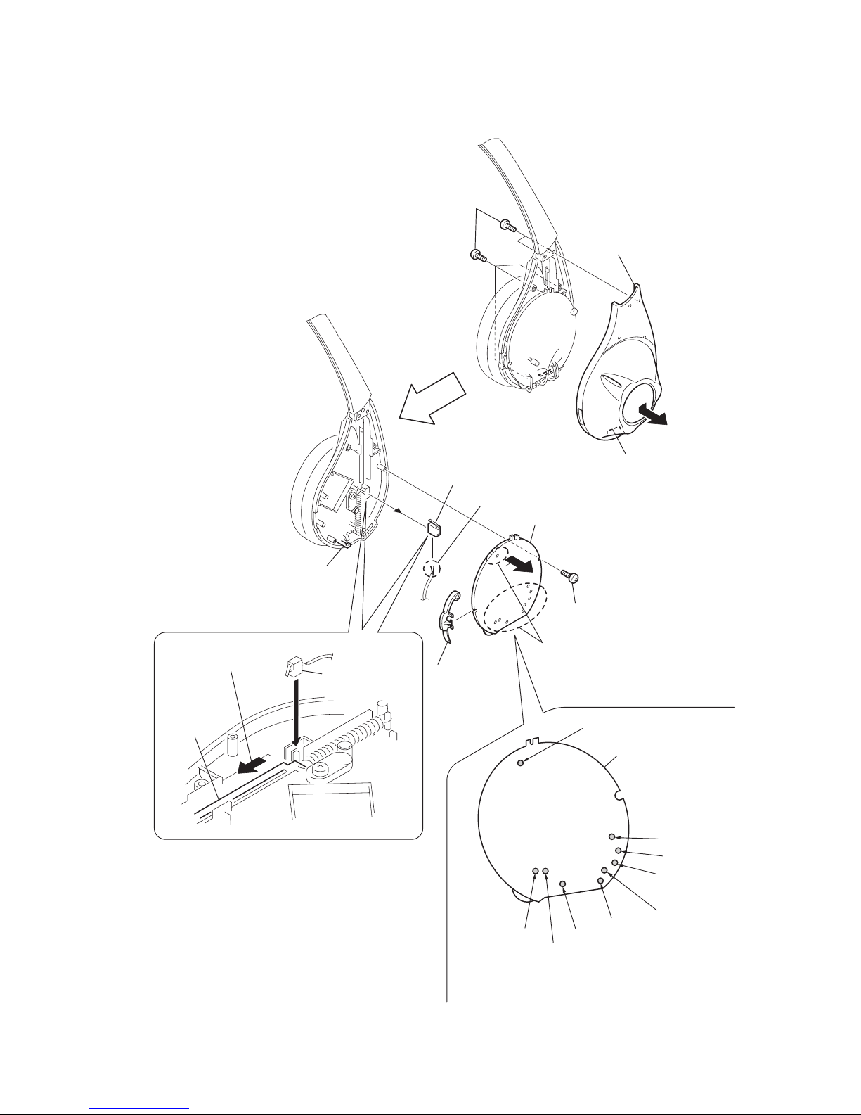
1. Use transmitter with check and adjustment already completed.
2. On adjusting the headphones section, use the transmitter as a
jig.
Headphones:MDR-RF845R
Transmitter:TMR-RF845R
Procedure:
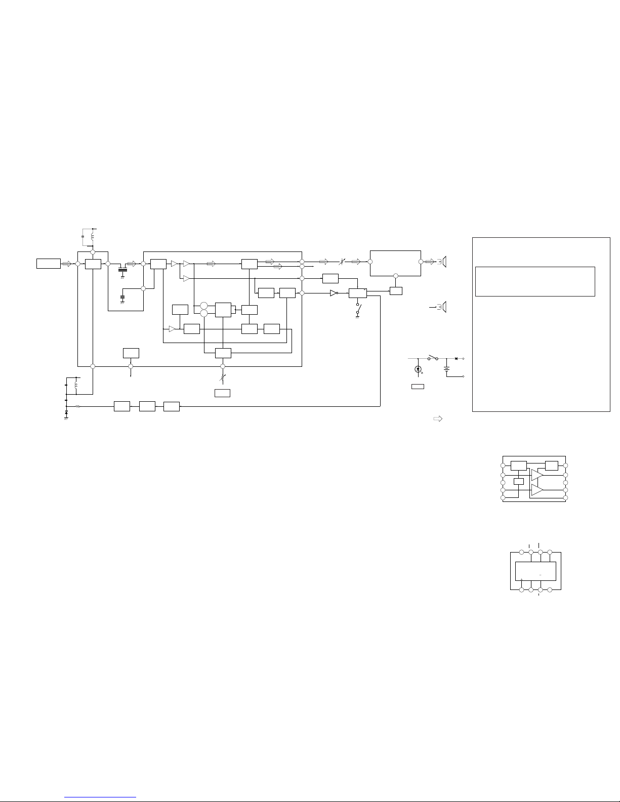
1. Connect an oscillator with attenuator and terminator (600 Ω)
to the transmitter AUDIO IN-A connector (J402).
2. Connect anAC adapter to the transmitter DC IN 9V jack (J404).
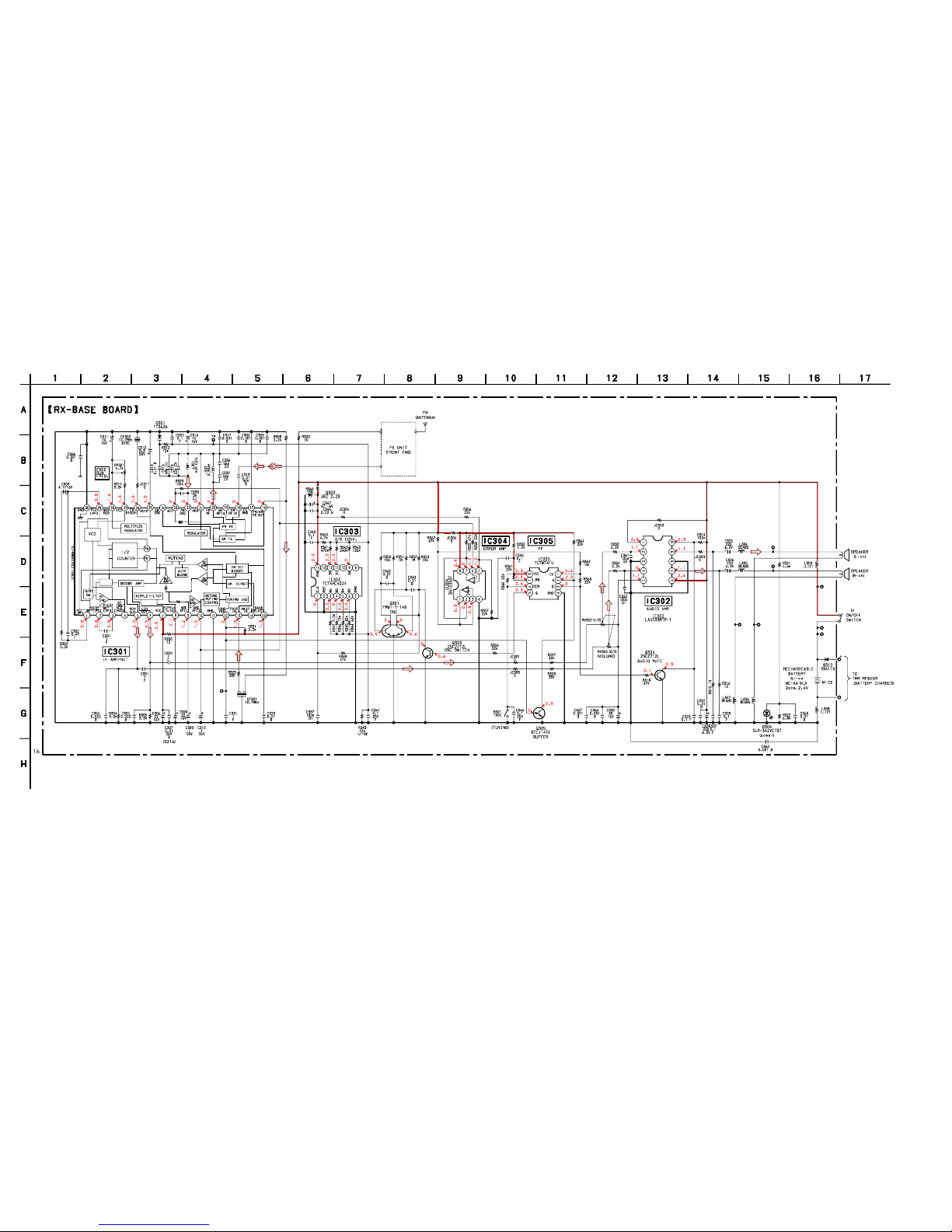
3. Short between Q303 corrector and GND on the RX board.
4. Connect a DC 2.4V to the +B power line externally.
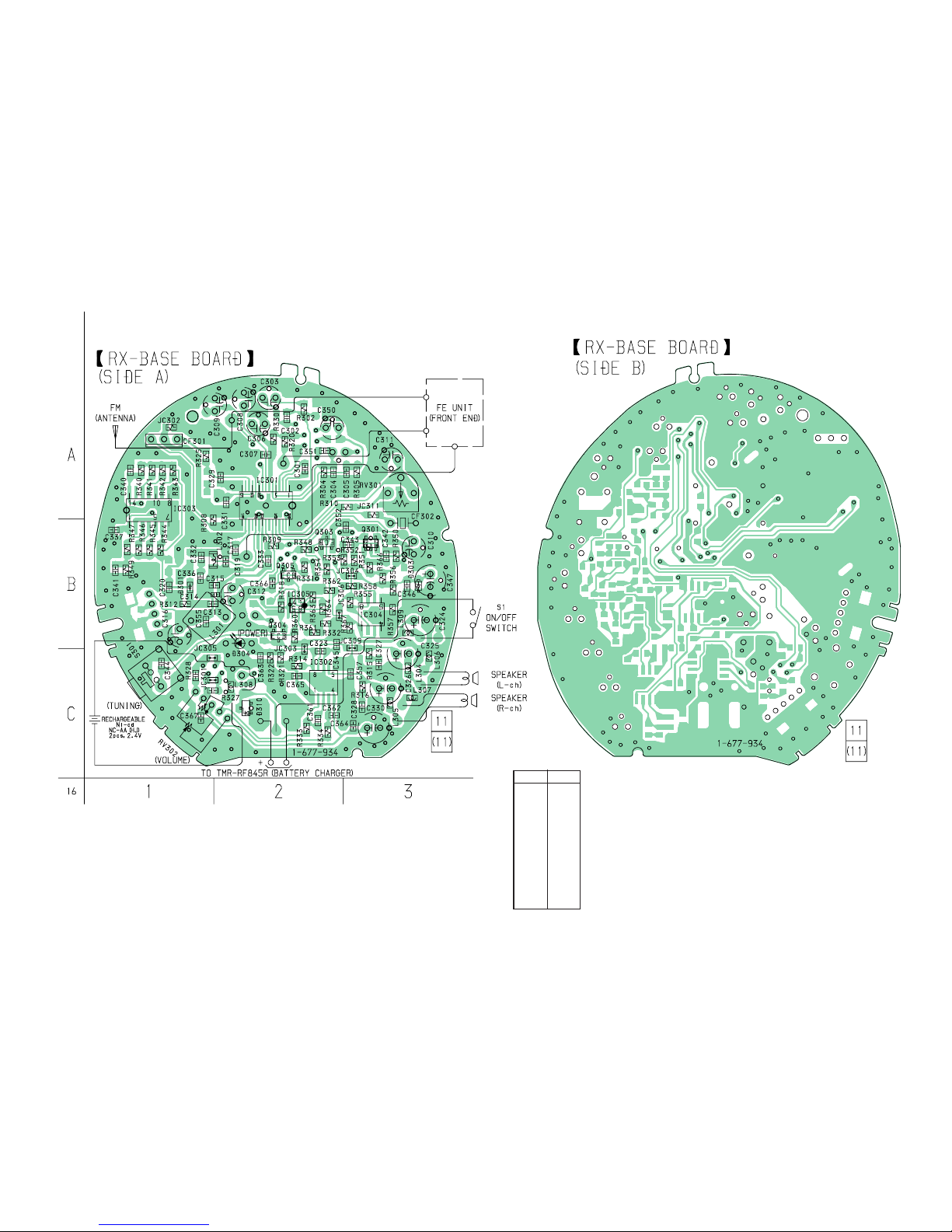
5. Connect lead wires to IC301 pin 4, pin 6, pin 7 and GND on
the RX-BASE board.
6. Connect a resistor 33k Ωbetween IC301 pin 4 and pin 7.
7. Connect lead wires to the speakers’ terminals (L+,L-,R+,R-)
on the RX-BASE board.
3-1. Free Run Frequency Check and Adjustment
1. Set the transmitter AUDIO IN-A connector (J402) to no signal.
Note: In this case, operation time is about 5 or 10 minutes.
Perform confirmation for less than 5 minutes.
2. Check the transmitter power indicator (red) lights.
3. Set the transmitter CHANNEL switch to 1.
4. Connect DC 1.2V across TP and GND.
5. Connect a frequency counter to IC301 pin 4 and GND on the
RX-BASE board, then confirm the frequency within 76kHz
±50Hz
6. When the frequency dose not satisfy the specified value, adjust
the value of the frequency counter to specification by RV301
on the RX-BASE board.
Specified values: 76kHz ±50Hz.
7. Remove the 33 kΩ resister between IC301 pin 4 and pin 7.
Setting :
3-2. Receive Frequency Check and Adjustment
1. Set the transmitter CHANNEL switch to 2.
2. Set the transmitter NOISE FILTER switch to OFF.
3. Input a signal of 1kHz, 316mVrms to transmitter AUDIO IN-
A(L-ch) connector only.
4. Keep distance between transmitter and headphones to 5 meters
over.
5. Set the headphones volume (RV302) to minimum.
6. Connect DC1.2V across TP and GND.
7. Connect an oscilloscope CH1 and CH2 to IC301 pin 6 and
pin 4.
8. Check the waveform of the oscilloscope to CH1 is demodulated
1kHz signal and CH2 is GND.
9. If CH1 and CH2 are not satisfied in step 8, adjust the coil (L301)
on the RX board to satisfied step 8.
10. Open between Q303 corrector and GND on the RX board.
11. When the transmitter off, check the waveform of the oscilloscope
as follows:
12. Set the transmitter CHANNEL switch to 1.
13. Push the headphones tuning switch (S301) to receive radio
frequency.
14. Check same step 8.
15. Set the transmitter CHANNEL switch to 3.
16. Push the headphones tuning switch (S301) to receive radio
frequency.
17. Check same step 8.
3-3. Carrier Modulation Check
1. Set the transmitter CHANNEL switch to 2.
2. Set the transmitter NOISE FILTER switch to OFF.
3. Input a signal of 1kHz, 316mVrms to transmitterAUDIO IN-A
(L-ch) connector only.
4. Set the headphones volume (RV302) to minimum.
5. Connect an oscilloscope CH1 and CH2 to IC301 pin 6 and
pin 4.
6. Push the headphone tuning switch (S301) to receive radio
frequency.
7. Check the waveform of the oscilloscope that the CH1 is
demodulated 1kHz signal and CH2 is GND.
8. Connect an AC voltmeter with LPF to IC301 pin 6 and GND.
9. Check the value of the AC voltmeter to 26mVrms ±2mV
Setting :
3-4. Separation Check
1. Set the transmitter CHANNEL switch to 2.
2. Set the transmitter NOISE FILTER switch to OFF.
3. Input a signal of 1kHz, 316mVrms to transmitterAUDIO IN-A
(L-ch) connector only.
4. Connect an oscilloscope CH1 to speakers terminal (L+,L-) and
CH2 to IC301 pin 4 and GND.
5. Push the headphones tuning switch (S301) to receive radio
frequency.
6. Check the waveform of the oscilloscope that the CH1 is
demodulated 1kHz signal and CH2 is GND.
7. Connect an AC voltmeter with LPF to speakers terminal
(L+,L-).
8. Adjust the value of the AC voltmeter to specification by
headphones volume RV302.
Specified values: 155mVrms
9. Connect an AC voltmeter with LPF to speakersterminal
(R+,R-).
10. Measure the value of the AC voltmeter.
11. Check the difference of the L and R to more than 20dB.
12. Input a signal of 1kHz, 316mVrms to transmitter AUDIO IN-A
(R-ch) connector only.
Setting :
IC301 pin4
GND
+
–
+
–
Regulated power supply
(DC 1.2V)
TP
Frequency counte
r
GND
1.8V
2-3sec 0.6V
+
–
Regulated power supply
(DC 1.2V)
TP
+
–
+
–
IC301 pin6 IC301 pin
4
OSCILLOSCPE
CH1 CH2
+
–
Digital voltmeter
(AC range)
LPF
IC301
pin6
33000P
2.2K
+
–
+
–
IC301 pin6 IC301 pin4
OSCILLOSCPE
CH1 CH2
13. Connect an AC voltmeter with LPF to speakers terminal
(R+,R-).
14. Adjust the value of the AC voltmeter to specification by
headphones volume RV302.
Specified values: 155mVrms
15. Connect an AC voltmeter with LPF to speakers terminal
(L+,L-).
16. Measure the value of the AC voltmeter.

—6 —
Adjustment Location :
[RX-BASE BOARD]
(Conductor side)
+
–
Digital voltmeter
(AC range)
L+ / R+
L–/ R–
+
–
+
–
L+ IC301 pin
4
OSCILLOSCPE
L–
CH1 CH2
17. Check the difference of the L and R to more than 20 dB.
Ver 1.2 2001. 11
IC301 7
IC301 4
IC301 6
GND
Short
L–
L+
R–
R+
GND
TP(R312-C320)
(Connect a 33k Ωresistor)
RV301:
Free Run Frequenc
y
Adjustment
+B
power line
(DC 2.4V)
RV302:
Volume control
L301:
Receive Frequency
Adjustment
S301:
TUNE switch

MDR-RF845R
4-1. BLOCK DIAGRAM
— 7 — — 8 —
L301
RECEIVE
FREQ.
D301
+V +V
FRONT END
FE UNIT 18 1316 FM IF/
DISCRI
DECODE
AMP
DETUNE
MUTE
TUNING
IND
STEREO
IND
CF301
26
CF302
10.7MHz
6 2
10
9
5R-CH
R-CH
RV302
VOLUME
SPEAKER
L-CH
SPEAKER
R-CH
POWER AMP
IC302
MUTE
Q304
22
20
FM FE
L302
+V
D/A
CONV
IC303
DETECT
IC304
FF
IC303
OSC
Q301
SWITCH
Q303
10
12
27
S301
TUNING
Q305
DQ
Q
AUTO
BLEND
MUTE MONO/ST
SW
1/2
COUNTER
PD1
PD1
VCO
21
REG
RV301
FREE RUN
FREQ.
IF AMP/DECODE
IC301
D304
S1
ON/OFF SW
+
-
B+
• Signal path.
: FM
16
POWER
SECTION 4
DIAGRAMS
• IC BLOCK DIAGRAMS
IC302 LA4533M
IC303 TC7W74FU
POWER
SWITCH
MUTE
CIRCIUT
BIAS
1
2
3
4
56
7
8
9
10 MT/SW
OUT1
POWER GND
OUT2
VCC
P/SW
IN1
PRE GND
IN2
REF
AMP2
AMP1
6
CLR
7
PR
8
VCC
5
Q
RSQ
3
Q
2
D
4
GND
1
CK
QDC
Note on Schematic Diagram:
• All capacitors are in µF unless otherwise noted. pF: µµF 50WV or
less are not indicated except for electrolytics and tantalums.
• All resistors are in Ωand 1/4W or less unless otherwise specified.
•¢: internal component.
•A: B+ Line.
•H: adjustment for repair.
• Power voltage is dc 2.4 V and fed with regulated dc power supply
from battery terminal.
• Voltages are dc with respect to ground under no-signal conditions.
• Voltages are taken with aVOM (Input impedance 10 MΩ).
Voltage variations may be noted due to normal production toler-
ances.
• Waveforms are taken with a oscilloscope.
Voltage variations may be noted due to normal production toler-
ances.
• Circled numbers refer to waveforms.
• Signal path.
F:FM
L: AUDIO
Note on Printed Wiring Board:
•X: parts extracted from the component side.
•®:Through hole.
•b: Pattern from the side which enables seeing.
Caution:
Pattern face side: Partsonthe pattern faceside seenfrom
(SideB) the pattern face are indicated.
Parts face side: Parts on the parts face side seen from
(Side A) the parts face are indicated.

MDR-RF845R
4-2. SCHEMATIC DIAGRAM
—9 — — 10 —

MDR-RF845R
4-3. PRINTEDWIRING BOARD
— 11 — — 12 —
Ref. No. Location
D301 B-1
D303 B-3
D304 B-2
D310 C-2
IC301 A-2
IC302 C-2
IC303 A-1
IC304 B-3
IC305 B-2
Q301 B-3
Q303 B-2
Q304 B-2
Q305 B-2
• Semiconductor
Location

MDR-RF845R
MEMO

— 13 —
SECTION 5
EXPLODED VIEWS
NOTE:
• -XX, -X mean standardized parts, so they may
have some differences from the original one.
• Items marked “*” are not stocked since they
are seldom required for routine service. Some
delay should be anticipated when ordering these
items.
• The mechanical parts with no reference number
in the exploded views are not supplied.
• Hardware (# mark) list and accessories and
packing materials are given in the last of this
parts list.
1
2
3
4
5
7
810
9
11
12
21
22
23
13
3
4
5
9
1415
6
#2
#1
#1
#1
#1
#1
#2
#2
#2
16
19
17
8
23
20
a
a
b
b
24
24
24
25
Ref. No. Part No. Description Remarks Ref. No. Part No. Description Remarks
1 3-046-672-01 SUSPENDER
2 3-046-671-01 BAND,HEAD
3 3-046-692-01 PAT,EAR
4 1-542-400-11 DRIVER (030F032)
5 3-046-685-01 PLATE(L), FRONT
6 3-046-675-01 HANGER (R)
7 1-771-249-11 SWITCH, PUSH (1 KEY)
8 4-992-281-01 HOLDER, BALL SHAFT
9 4-981-975-01 SPRING, FREE ADJUSTMENT
*10 A-4542-649-A RX-BASE BOARD, COMPLETE
11 3-046-677-01 COVER (R), HANGER
12 3-049-799-01 LIGHT, MDR GUIDE
13 3-046-679-01 CAP(R), ORNAMENTAL
14 3-046-674-01 HANGER (L)
15 3-048-267-01 TERMINAL (MIDWAY), BATTERY
16 3-048-265-01 TERMINAL (+), BATTERY
17 3-048-266-01 TERMINAL (-), BATTERY
19 3-046-676-01 COVER (L), HANGER
20 3-046-678-01 CAP(L), ORNAMENTAL
21 3-046-682-01 TERMINAL, CHARGE
22 3-046-680-01 BUTTON, TUNING
23 3-048-264-01 SHEET, ORNAMENTAL CAP ADHESIVE
24 3-223-909-01 SCREW (B2)
25 1-756-112-11 BATTERY, NICKEL CADMIUM
#1 7-685-104-19 SCREW +P2X6 TYPE2 NON-SLIT
#2 7-685-105-19 SCREW +P2X8 TYPE2 NON-SLIT
Ver 1.12000. 11

— 13 — — 14 —
SECTION 5
EXPLODED VIEWS
NOTE:
• -XX, -X mean standardized parts, so they may
have some differences from the original one.
• Items marked “*” are not stocked since they
are seldom required for routine service. Some
delay should be anticipated when ordering these
items.
• The mechanical parts with no reference number
in the exploded views are not supplied.
• Hardware (# mark) list and accessories and
packing materials are given in the last of this
parts list.
1
2
3
4
5
7
810
9
11
12
21
22
23
13
3
4
5
9
1415
6
#2
#1
#1
#1
#1
#1
#2
#2
#2
16
19
17
8
23
20
a
a
b
b
24
24
24
25
Ref. No. Part No. Description Remarks Ref. No. Part No. Description Remarks
1 3-046-672-01 SUSPENDER
2 3-046-671-01 BAND,HEAD
3 3-046-692-01 PAT,EAR
4 1-542-400-11 DRIVER (030F032)
5 3-046-685-01 PLATE(L), FRONT
6 3-046-675-01 HANGER (R)
7 1-771-249-11 SWITCH, PUSH (1 KEY)
8 4-992-281-01 HOLDER, BALL SHAFT
9 4-981-975-01 SPRING, FREE ADJUSTMENT
*10 A-4542-649-A RX-BASE BOARD, COMPLETE
11 3-046-677-01 COVER (R), HANGER
12 3-049-799-01 LIGHT, MDR GUIDE
13 3-046-679-01 CAP(R), ORNAMENTAL
14 3-046-674-01 HANGER (L)
15 3-048-267-01 TERMINAL (MIDWAY), BATTERY
16 3-048-265-01 TERMINAL (+), BATTERY
17 3-048-266-01 TERMINAL (-), BATTERY
19 3-046-676-01 COVER (L), HANGER
20 3-046-678-01 CAP(L), ORNAMENTAL
21 3-046-682-01 TERMINAL, CHARGE
22 3-046-680-01 BUTTON, TUNING
23 3-048-264-01 SHEET, ORNAMENTAL CAP ADHESIVE
24 3-223-909-01 SCREW (B2)
25 1-756-112-11 BATTERY, NICKEL CADMIUM
#1 7-685-104-19 SCREW +P2X6 TYPE2 NON-SLIT
#2 7-685-105-19 SCREW +P2X8 TYPE2 NON-SLIT
Ref. No. Part No. Description Remarks Ref. No. Part No. Description Remarks
SECTION 6
ELECTRICAL PARTS LIST
NOTE:
•Due to standardization, replacements in the
parts list may be different from the parts
specified in the diagrams or the components
used on the set.
•-XX, -X mean standardized parts, so they
may have some difference from the original
one.
•Items marked “*”are not stocked since they
are seldom required for routine service.
Some delay should be anticipated when
ordering these items.
•CAPACITORS:
uF: µF
•RESISTORS
All resistors are in ohms.
METAL: metal-film resistor
METAL OXIDE: Metal Oxide-film resistor
F: nonflammable
•COILS
uH: µH
•SEMICONDUCTORS
In each case, u: µ, for example:
uA...: µA... , uPA... , µPA... ,
uPB... , µPB... , uPC... , µPC... ,
uPD..., µPD...
When indicating parts by reference number,
please include the board name.
*A-4542-649-A RX-BASE BOARD, COMPLETE
************************
*A-4542-642-A RX-FE UNIT (FRONT END)
< CAPACITOR >
C301 1-164-346-11 CERAMIC CHIP 1uF 16V
C302 1-164-005-11 CERAMIC CHIP 0.47uF 25V
C303 1-124-259-11 ELECT 4.7uF 20.00% 16V
C304 1-163-037-11 CERAMIC CHIP 0.022uF 10% 25V
C305 1-163-037-11 CERAMIC CHIP 0.022uF 10% 25V
C306 1-124-234-00 ELECT 22uF 20% 16V
C307 1-163-059-91 CERAMIC CHIP 0.01uF 10.00% 50V
C308 1-124-234-00 ELECT 22uF 20% 16V
C309 1-104-942-11 ELECT 1uF 20.00% 50V
C310 1-104-942-11 ELECT 1uF 20.00% 50V
C311 1-124-233-11 ELECT 10uF 20.00% 16V
C312 1-126-162-11 ELECT 3.3uF 20% 50V
C313 1-163-021-91 CERAMIC CHIP 0.01uF 10.00% 50V
C314 1-164-441-11 CERAMIC CHIP 68PF 5.00% 50V
C315 1-163-235-11 CERAMIC CHIP 22PF 5.00% 50V
C316 1-124-233-11 ELECT 10uF 20.00% 16V
C317 1-163-009-11 CERAMIC CHIP 0.001uF 10% 50V
C319 1-163-021-91 CERAMIC CHIP 0.01uF 10.00% 50V
C320 1-163-038-00 CERAMIC CHIP 0.1uF 25V
C323 1-163-038-00 CERAMIC CHIP 0.1uF 25V
C324 1-124-635-00 ELECT 220uF 20.00% 6.3V
C325 1-124-635-00 ELECT 220uF 20.00% 6.3V
C326 1-124-635-00 ELECT 220uF 20.00% 6.3V
C327 1-163-038-00 CERAMIC CHIP 0.1uF 25V
C328 1-163-038-00 CERAMIC CHIP 0.1uF 25V
C329 1-163-021-91 CERAMIC CHIP 0.01uF 10.00% 50V
C330 1-124-242-00 ELECT 33uF 20% 25V
C331 1-164-346-11 CERAMIC CHIP 1uF 16V
C332 1-163-245-11 CERAMIC CHIP 56PF 5.00% 50V
C333 1-163-220-11 CERAMIC CHIP 3PF 0.25PF 50V
C336 1-163-245-11 CERAMIC CHIP 56PF 5.00% 50V
C337 1-163-251-11 CERAMIC CHIP 100PF 5.00% 50V
C340 1-163-038-00 CERAMIC CHIP 0.1uF 25V
C341 1-163-038-00 CERAMIC CHIP 0.1uF 25V
C342 1-163-021-91 CERAMIC CHIP 0.01uF 10.00% 50V
C343 1-163-021-91 CERAMIC CHIP 0.01uF 10.00% 50V
C344 1-163-038-00 CERAMIC CHIP 0.1uF 25V
C345 1-163-038-00 CERAMIC CHIP 0.1uF 25V
C346 1-164-489-11 CERAMIC CHIP 0.22uF 10.00% 16V
C347 1-124-589-11 ELECT 47uF 20% 16V
C350 1-164-346-11 CERAMIC CHIP 1uF 16V
C351 1-164-346-11 CERAMIC CHIP 1uF 16V
C352 1-163-009-11 CERAMIC CHIP 0.001uF 10% 50V
C355 1-163-009-11 CERAMIC CHIP 0.001uF 10% 50V
C357 1-163-021-91 CERAMIC CHIP 0.01uF 10.00% 50V
C361 1-163-251-11 CERAMIC CHIP 100PF 5.00% 50V
C362 1-163-251-11 CERAMIC CHIP 100PF 5.00% 50V
C363 1-163-021-91 CERAMIC CHIP 0.01uF 10.00% 50V
C364 1-163-009-11 CERAMIC CHIP 0.001uF 10% 50V
C365 1-163-009-11 CERAMIC CHIP 0.001uF 10% 50V
C366 1-163-009-11 CERAMIC CHIP 0.001uF 10% 50V
C367 1-163-009-11 CERAMIC CHIP 0.001uF 10% 50V
< FILTER >
CF301 1-577-588-11 FILTER, CERAMIC 10.7MHz
CF302 1-577-572-11 FILTER, CERAMIC 10.7MHz
< DIODE >
D301 8-719-110-48 DIODE RD18ESB1
D303 8-719-045-99 DIODE RD2.2M-T1B
D304 8-719-077-16 LED TLSU124 (power)
D310 8-719-975-40 DIODE RB411D
< IC >
IC301 8-752-072-12 IC CXA1538N
IC302 8-759-802-75 IC LA4533M
IC303 8-759-453-43 IC TC74HC4024AF(EL)
IC304 8-759-510-73 IC BA10393F-E2
IC305 8-759-083-94 IC TC7W74FU
< JUMPER >
JC301 1-216-295-91 SHORT 0
JC302 1-216-295-91 SHORT 0
JC303 1-216-295-91 SHORT 0
JC304 1-216-295-91 SHORT 0
JC305 1-216-295-91 SHORT 0
JC306 1-216-295-91 SHORT 0
JC309 1-216-295-91 SHORT 0
JC311 1-216-295-91 SHORT 0
< COIL >
L301 1-422-317-31 COIL, AIR-CORE
L302 1-412-933-11 INDUCTOR 0.33uH
L304 1-414-234-11 INDUCTOR CHIP 0uH
L305 1-414-234-11 INDUCTOR CHIP 0uH
L306 1-414-234-11 INDUCTOR CHIP 0uH
L307 1-414-234-11 INDUCTOR CHIP 0uH
L308 1-414-766-21 INDUCTOR CHIP 0uH
L309 1-414-766-21 INDUCTOR CHIP 0uH
RX-BASE
Ver 1.1 2000. 11

Ref. No. Part No. Description Remarks Ref. No. Part No. Description Remarks
— 15 —
< TRANSISTOR >
Q301 8-729-903-10 TRANSISTOR FMW1
Q303 8-729-230-49 TRANSISTOR 2SC2712-YG
Q304 8-729-230-49 TRANSISTOR 2SC2712-YG
Q305 8-729-027-44 TRANSISTOR DTC114TKA-T146
< RESISTOR >
R302 1-216-057-00 METAL CHIP 2.2K 5% 1/10W
R304 1-216-061-00 METAL CHIP 3.3K 5% 1/10W
R305 1-216-061-00 METAL CHIP 3.3K 5% 1/10W
R308 1-216-057-00 METAL CHIP 2.2K 5% 1/10W
R309 1-216-097-91 RES-CHIP 100K 5% 1/10W
R310 1-216-061-00 METAL CHIP 3.3K 5% 1/10W
R312 1-216-077-00 RES-CHIP 15K 5% 1/10W
R314 1-216-097-91 RES-CHIP 100K 5% 1/10W
R315 1-216-001-00 METAL CHIP 10 5% 1/10W
R316 1-216-001-00 METAL CHIP 10 5% 1/10W
R318 1-216-089-91 RES-CHIP 47K 5% 1/10W
R320 1-216-001-00 METAL CHIP 10 5% 1/10W
R321 1-216-053-00 METAL CHIP 1.5K 5% 1/10W
R322 1-216-069-00 METAL CHIP 6.8K 5% 1/10W
R325 1-216-037-00 METAL CHIP 330 5% 1/10W
R327 1-216-085-00 METAL CHIP 33K 5% 1/10W
R328 1-216-085-00 METAL CHIP 33K 5% 1/10W
R330 1-216-001-00 METAL CHIP 10 5% 1/10W
R331 1-216-057-00 METAL CHIP 2.2K 5% 1/10W
R332 1-216-049-91 RES-CHIP 1K 5% 1/10W
R333 1-216-057-00 METAL CHIP 2.2K 5% 1/10W
R334 1-216-057-00 METAL CHIP 2.2K 5% 1/10W
R340 1-216-065-91 RES-CHIP 4.7K 5% 1/10W
R341 1-216-113-00 METAL CHIP 470K 5% 1/10W
R342 1-216-106-00 METAL CHIP 240K 5% 1/10W
R343 1-216-099-00 METAL CHIP 120K 5% 1/10W
R344 1-216-092-00 RES-CHIP 62K 5% 1/10W
R345 1-216-084-00 METAL CHIP 30K 5% 1/10W
R346 1-216-077-00 RES-CHIP 15K 5% 1/10W
R347 1-216-070-00 METAL CHIP 7.5K 5% 1/10W
R348 1-216-089-91 RES-CHIP 47K 5% 1/10W
R349 1-216-073-00 METAL CHIP 10K 5% 1/10W
R350 1-216-077-00 RES-CHIP 15K 5% 1/10W
R351 1-216-121-91 RES-CHIP 1M 5% 1/10W
R352 1-216-121-91 RES-CHIP 1M 5% 1/10W
R353 1-216-077-00 RES-CHIP 15K 5% 1/10W
R354 1-216-081-00 METAL CHIP 22K 5% 1/10W
R355 1-216-089-91 RES-CHIP 47K 5% 1/10W
R356 1-216-081-00 METAL CHIP 22K 5% 1/10W
R357 1-216-081-00 METAL CHIP 22K 5% 1/10W
R358 1-216-081-00 METAL CHIP 22K 5% 1/10W
R360 1-216-081-00 METAL CHIP 22K 5% 1/10W
R361 1-216-081-00 METAL CHIP 22K 5% 1/10W
R362 1-216-073-00 METAL CHIP 10K 5% 1/10W
R363 1-216-081-00 METAL CHIP 22K 5% 1/10W
R364 1-216-081-00 METAL CHIP 22K 5% 1/10W
R366 1-216-029-00 METAL CHIP 150 5% 1/10W
R367 1-216-089-91 RES-CHIP 47K 5% 1/10W
< VARIABLE RESISTOR >
RV301 1-241-763-11 RES, ADJ, CARBON 4.7K
RV302 1-227-189-11 RES, VAR CARBON 20K/20K (VOLUME)
< SWITCH >
S301 1-771-980-11 SWITCH, TACTILE (TUNING)
**************************************************************
MISCELLANEOUS
**************
4 1-542-400-11 DRAIVER (030F032)
7 1-771-249-11 SWITCH, PUSH (1 KEY)
**************************************************************
RX-BASE

MDR-RF845R
REVISION HISTORY
Clicking the version allows you to jump to the revised page.
Also, clicking the version at the upper right on the revised page allows you to jump to the next revised
page.
Ver. Date Description of Revision
1.2 2001.01 Correction of electrical adjustments
1.1 2000.11 Change of exploded view
1.0 2000.06 New
(ENG-01023)
(ENG-00019)
This manual suits for next models
1
Table of contents
Other Sony Headphones manuals

Sony
Sony MDR-XB20EX User manual

Sony
Sony MDR-110LP Installation instructions manual

Sony
Sony MDR-EX85LP User manual

Sony
Sony MDR-ZX700 User manual

Sony
Sony MDR SA3000 User manual

Sony
Sony MDR-ZX600 User manual

Sony
Sony MDR-RF975RK User manual

Sony
Sony MDR-NE5 User manual

Sony
Sony MDR-CD280 User manual

Sony
Sony MDR-1ADAC Guide

Sony
Sony MDREX10LP/GRN User manual

Sony
Sony DR-E10iP/VLT User manual

Sony
Sony MDR-NC13 User manual

Sony
Sony MDR-AS200 User manual

Sony
Sony MDR-MA100 User manual

Sony
Sony MDR-RF810RK User manual

Sony
Sony MDR-RF5000K User manual

Sony
Sony MDR-1RBT Use and maintenance manual

Sony
Sony MDR-PQ4 User manual

Sony
Sony MDR-1AM2 User manual