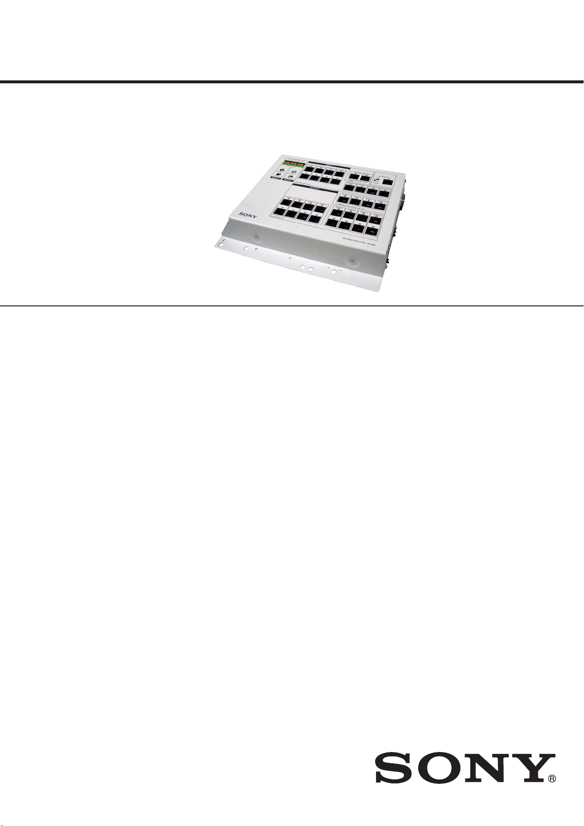
Sony HS-MB1 User manual

SERVICE MANUAL
Sony Corporation
Audio&Video Business Group
Published by Sony Techno Create Corporation
HS-MB1
DISTRIBUTION PANEL
9-889-410-01
2009B04-1
© 2009.02
US Model
Ver. 1.0 2009.02
SPECIFICATIONS
Input and output terminals
RJ45: T568B Terminated. ABE (only for connection to HS-KP1
(Keypad))
(ADC 19.5 V included)
CD (only for connection to HS-WV1
(AV Wall Port))
(CDC 19.5 V included)
F(only for connection to CAV-CVB1
(Component Video Balun))
(DC 10 V included)
GH (only for connection to HS-WD1
(DIGITAL MEDIA Wall Port))
(GDC 19.5 V included)
40 pin flat terminals: For IDE cable (with pin 20 opening) only
(For stack connection only)
Pin jack video in: For camera 1, 2 NTSC 75 ohms terminal
DC IN: HS-AC1 only (not supplied)
10 V: by JEITA TYPE4 Jacks
19.5 V: by JEITA TYPE5 Jacks
DB1, DB2, CHIME: Wire requirements: Copper Wire AWG 26 - 18
Outer diameter: 3 mm (0.12 inches), maximum
Strip away: 10 mm (0.4 inches)
RS-232C (DB9 Straight): For stack connection and service only
GENERAL
DC Power consumption (when HS-KP1, HS-WV1, HS-WA1,HS-WD1,
and CAV-CVB1 are not connected):
DC 19.5 V /0.6 A (ZONE 1 - 4), 0.1 A
(ZONE 5 - 8)
DC 10 V /0.3 A
* Use DC 19.5 V for HS-KP1, HS-WV1, HS-WA1, HS-WD1, and
CAV-CVB1.
For details, refer to the instruction manual of each product.
* Use DC 10 V only for HS-MB1. Even if you connect the DC 10 V to
HS-MB1, no power is supplied HS-KP1, HS-WV1, HS-WA1, HS-
WD1, or CAV-CVB1.
Operating temperature: 0 ˚C - 30 ˚C (32 ˚F - 86 ˚F)
Storage temperature: –20 °C - 60 °C (–4 °F - 140 °F)
Dimensions: 290 × 250 × 55 mm
(11
1/22 × 9 7/8× 21 3/4inches) (w/h/d)
Mass: 2 kg (4 lbs 6 1/2 oz.)
Supplied accessories
HS-AC1
AC power cord (mains lead)
Installer’s manual
Design and specifications are subject to change without notice.
• HS-AC1 is attached to HS-MB1.
Please refer to service manual of
HS-AC1 for information on HS-AC1.

HS-MB1
2
SAFETY-RELATED COMPONET WARNING!
COMPONENTS IDENTIFIED BY MARK 0OR DOTTED LINE
WITH MARK 0ON THE SCHEMATIC DIAGRAMS AND IN
THE PARTS LIST ARE CRITICAL TO SAFE OPERATION.
REPLACE THESE COMPONENTS WITH SONY PARTS
WHOSE PART NUMBERS APPEAR AS SHOWN IN THIS
MANUAL OR IN SUPPLEMENTS PUBLISHED BY SONY.
UNLEADED SOLDER
Boards requiring use of unleaded solder are printed with the lead-
free mark (LF) indicating the solder contains no lead.
(Caution: Some printed circuit boards may not come printed with
the lead free mark due to their particular size)
: LEAD FREE MARK
Unleaded solder has the following characteristics.
• Unleaded solder melts at a temperature about 40 °C higher
than ordinary solder.
Ordinary soldering irons can be used but the iron tip has to be
applied to the solder joint for a slightly longer time.
Soldering irons using a temperature regulator should be set to
about 350 °C.
Caution: The printed pattern (copper foil) may peel away if
the heated tip is applied for too long, so be careful!
• Strong viscosity
Unleaded solder is more viscous (sticky, less prone to flow)
than ordinary solder so use caution not to let solder bridges
occur such as on IC pins, etc.
• Usable with ordinary solder
It is best to use only unleaded solder but unleaded solder may
also be added to ordinary solder.
NOTES ON CHIP COMPONENT REPLACEMENT
• Never reuse a disconnected chip component.
• Notice that the minus side of a tantalum capacitor may be dam-
aged by heat.
1. SERVICE NOTE ....................................................... 3
2. GENERAL................................................................... 4
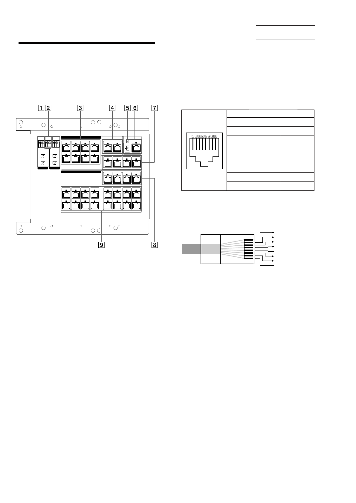
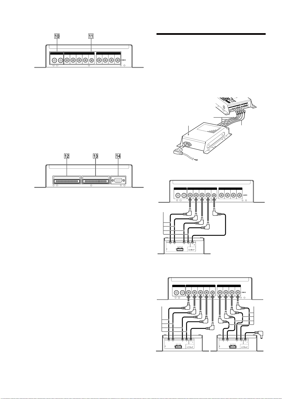
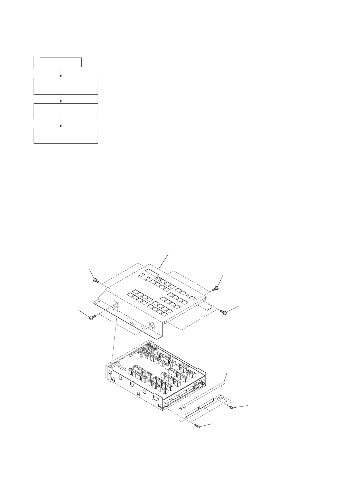
3. DISASSEMBLY
3-1. Case (MB)....................................................................... 8
3-2. VIDEO Board................................................................. 9
3-3. MAIN Board................................................................... 9
4. DIAGRAMS
4-1. Block Diagram –Audio Select Section–......................... 11
4-2. Block Diagram –Mic Select Section–............................. 12
4-3. Block Diagram –Video Select Section–.......................... 13
4-4. Block Diagram –Zone SW Section–............................... 14
4-5. Block Diagram –RS-232C Section–............................... 15
4-6. Block Diagram –Video Section– .................................... 16
4-7. Block Diagram –Power Section–.................................... 17
4-8. Printed Wiring Board –Main Section (1/2)–................... 18
4-9. Printed Wiring Board –Main Section (2/2)–................... 19
4-10. Schematic Diagram –Main Section (1/5)–...................... 20
4-11. Schematic Diagram –Main Section (2/5)–...................... 21
4-12. Schematic Diagram –Main Section (3/5)–...................... 22
4-13. Schematic Diagram –Main Section (4/5)–...................... 23
4-14. Schematic Diagram –Main Section (5/5)–...................... 24
4-15. Printed Wiring Board –Video Section (1/2)–.................. 25
4-16. Printed Wiring Board –Video Section (2/2)–.................. 26
4-17. Schematic Diagram –Video Section (1/7)–..................... 27
4-18. Schematic Diagram –Video Section (2/7)–..................... 28
4-19. Schematic Diagram –Video Section (3/7)–..................... 29
4-20. Schematic Diagram –Video Section (4/7)–..................... 30
4-21. Schematic Diagram –Video Section (5/7)–..................... 31
4-22. Schematic Diagram –Video Section (6/7)–..................... 32
4-23. Schematic Diagram –Video Section (7/7)–..................... 33
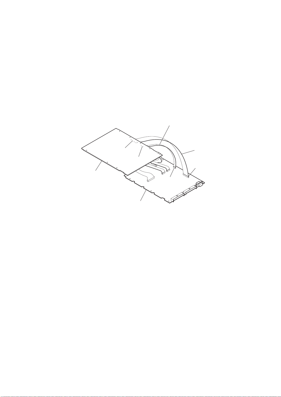
5. EXPLODED VIEW
5-1. Main Section................................................................... 41
6. ELECTRICAL PARTS LIST.............................. 42
TABLE OF CONTENTS
SAFETY CHECK-OUT
After correcting the original service problem, perform the follow-
ing safety check before releasing the set to the customer:
Check the antenna terminals, metal trim, “metallized” knobs,
screws, and all other exposed metal parts for AC leakage.
Check leakage as described below.
LEAKAGE TEST
The AC leakage from any exposed metal part to earth ground and
from all exposed metal parts to any exposed metal part having a
return to chassis, must not exceed 0.5 mA (500 microamperes.).
Leakage current can be measured by any one of three methods.
1. Acommercial leakage tester, such as the Simpson 229 or RCA
WT-540A. Follow the manufacturers’ instructions to use these
instruments.
2. A battery-operated AC milliammeter. The Data Precision 245
digital multimeter is suitable for this job.
3. Measuring the voltage drop across a resistor by means of a
VOM or battery-operatedAC voltmeter. The “limit” indication
is 0.75 V, so analog meters must have an accurate low-voltage
scale. The Simpson 250 and Sanwa SH-63Trd are examples
of a passive VOM that is suitable. Nearly all battery operated
digital multimeters that have a 2 VAC range are suitable. (See
Fig. A)
1.5 kΩ0.15 μFAC
voltmeter
(0.75 V)
To Exposed Metal
Parts on Set
Earth Ground
Fig. A. Using an AC voltmeter to check AC leakage.

HS-MB1
3
SECTION 1
SERVICE NOTE
NOTE FOR REPAIRING THE HS-MB1
The HS-MB1 cannot be repaired singly since it has no power
supply.
It should be connected with the HS-AC1 when servicing/repair-
ing it.
EXTENTION CABLE AND SERVICE POSITION
When repairing or servicing this set, connect the jig (extention
cable) as shown below.
• Connect the MAIN board (CN2975) and the VIDEO board
(CN705) with the extention cable (Part No. J-2501-199-A).
Connect the MAIN board (CN2510) and the VIDEO board
(CN1110) with the extention cable (Part No. 1-828-223-11).
J-2501-199-A
1-828-223-11
CN705
CN1110
CN2975
MAIN board
VIDEO board CN2510

HS-MB1
4
SECTION 2
GENERAL This section is extracted
from instruction manual.
Hooking up the HS-MB1
Before hooking up the HS-MB1, be sure the AC power cord is
unplugged.
Note
If a CAT5 cable is connected to the wrong RJ45 terminal, units or devices
connected to HS-MB1 may be damaged when you plug in the AC power cord.
Termin a ls ",$,', and (supply DC voltage, so make sure of all connections
before plugging in the AC power cord.
ZONE 1
A
B
ZONE 2
A
B
ZONE 3
A
B
ZONE 4
A
B
ZONE 5
A
B
ZONE 6
A
B
ZONE 7
A
B
ZONE 8
A
B
TO KEYPAD HS-KP1
TO AV WALL PORT H S- WV1
TO COMPONENT VIDEO BALUN CAV-CVB1
TO DIGITAL MEDIA WALL PORT
HS-WD1
OUTPUT
DOOR 2
INPUT
ZONE 1
F
ZONE 2
F
ZONE 3
F
ZONE 4
F
SOURCE 1
E
SOURCE 2
E
SOURCE 3
E
SOURCE 4
E
SOURCE 1
C
D
SOURCE 2
C
D
SOURCE 3
C
D
SOURCE 4
C
D
G
SOURCE DMPORT
HB
SERVICE
ZONE
LOCAL
MODE
DB2
OFF 2 3
2E1
DB1
2E1
CHIME
2E1
GAIN
123
DOOR 1
MODE
OFF 2 3
GAIN
123
DB1/DB2
Connect the conductor cable for Doorbell.
MODE: Set 2 or 3 depending on the Doorbell manufacturer.
GAIN: Set the mic/speaker level of the Doorbell.
CHIME
Connect the external chime.
INPUT
SOURCE 1 ~ 4 $%
RJ45 terminals to input audio signal from AV Wall Port(s)
(HS-WV1).
Use both terminals for the connection.
Note
When you connect a Multi Channel AV Receiver to the HS-MB1, be sure to
use the SOURCE 1 terminals. e Multi Channel AV Receiver will not work
with the SOURCE 2, 3, or 4 terminals.
SOURCE DMPORT ()
RJ45 terminals to input Digital Media Port signal from Digital Media
Wall Port(s) (HS-WD1).
Use both terminals for the connection.
Note
If a DIGITAL MEDIA PORT adapter is connected to a Multi Channel AV
Receiver which is connected to the HS-MB1, you cannot use the SOURCE
DMPORT terminals of the HS-MB1.
DC IN indicator
SERVICE #
RJ45 terminals for Keypad (HS-KP1) rmware updates.
ZONE: Select this when updating the Keypad (HS-KP1) rmware.
LOCAL: Select this when updating this unit’s rmware.
SOURCE 1 ~ 4 &
RJ45 terminals to input video signal from AV Wall Port(s)
(HS-WV1).
OUTPUT
ZONE 1 ~ 4 '
RJ45 terminals send a video signal source to the component video.
Use a Component Video Balun (CAV-CVB1) for the connection.
CAT5 RJ45 Pinout
When you connect the Component Video Balun (CAV-CVB1), the
CAT5 RJ45 pinouts use the T568B standard. Refer to the illustration
below.
Pinout Wire color
Pin 1 BLUE/Pb (R) White/Orange
Pin 2 BLUE/Pb (T) Orange
Pin 3 GREEN/Y (R) White/Green
Pin 4 GND Blue
Pin 5 +11V White/Blue
Pin 6 GREEN/Y (T) Green
Pin 7 RED/Pr (R) White/Brown
Pin 8 RED/Pr (T) Brown
CAT5 cable
Be sure to use Category 5e straight-through cables, and the wiring
connection is correct. See the illustration below for details on
connections.
White/Orange
Wire color
Orange
White/Green
Blue
White/Blue
Green
White/Brown
Brown
1
Pin No.
2
3
4
5
6
7
8
ZONE 1 ~ 8 "#
RJ45 terminals for Keypad (HS-KP1).
Use both terminals for the connection.
Note
If you use the ZONE 5 ~ 8 terminals, you need to connect the additional
Power Supply (HS-AC1) (optional) to ZONE 5 – 8 DC IN.
Note on installing CAT5 cables
e following lengths of cable(s) can extend up to 200 feet:
●e combined length of the two longest cables connecting the HS-MB1 to an
AV Wall Port (HS-WV1) and a Keypad (HS-KP1).
●e combined length of the cable connecting the HS-MB1 to the Digital Media
Wall Port (HS-WD1) and the longest cable connecting to a Keypad (HS-KP1).
●e length of the longest cable connecting the HS-MB1 to a Component Video
Balun (CAV-CVB1).

HS-MB1
5
1
IN
2
10V19.5V
ZONE 1
19.5V
ZONE 2
19.5V
ZONE 3
19.5V
ZONE 4
DC IN
CAMERA
19.5V
ZONE 5
19.5V
ZONE 6 ZONE 7
19.5V 19.5V
ZONE 8
DC IN
+CAMERA 1/2 IN jack
Pin jack for video input from a video camera.
,DC IN
Connect the DC IN terminals using the Power Supply (HS-AC1)
(supplied).
ZONE 1 – 4: Connect all four of the 19.5 V plugs and the 10 V plug
of the Power Supply (HS-AC1) (supplied). e ZONE 1
19.5 V cable also supplies power to the HS-MB1 main
unit.
ZONE 5 – 8: If you use the ZONE 5 ~ 8 terminals in addition to the
ZONE 1 ~ 4 terminals, connect all four of the 19.5 V
plugs of a second Power Supply (HS-AC1) (optional).
e 10 V plug of this second Power Supply (HS-AC1)
(optional) is not used.
ZONE EXPANSION OUT ZONE EXPANSION IN RS-232C
-ZONE EXPANSION OUT
IDE (Integrated Drive Electronics) terminal for sending a source to
another Distribution Panel (HS-MB1). Use an IDE cable (not
supplied) for the connection.
.ZONE EXPANSION IN
IDE (Integrated Drive Electronics) terminal to input a source from
another Distribution Panel (HS-MB1). Use an IDE cable (not
supplied) for the connection.
Note
Only if another Distribution Panel (HS-MB1) is connected for expansion is
its ZONE EXPANSION IN terminal used.
/RS-232C
Connect to a computer for rmware updates or addition of another
Distribution Panel (HS-MB1) (Stack connection). Use an RS-232C
cross cable (not supplied) for connection.
Note
With another Distribution Panel (HS-MB1), you can connect 16 units
maximum in one system network. All units can receive audio sources. Each
unit in zone 1, 2, 3, and 4 can accept video sources. However, if you use two
Distribution Panels (HS-MB1) in one system network, available input sources
are up to four.
Connecting the AC power cord
Before connecting the AC power cord to a wall outlet, connect all parts
of the system to the unit. e indicator lights green when the AC power
cord is connected to the wall outlet and the HS-MB1 is engaged.
Notes
●Aer completing all the connections, make sure there are no misconnections or
improper wiring before plugging the Power Supply (HS-AC1) (supplied) into
the wall outlet. Improper wiring or misconnections may cause damage to the
unit.
●Use the Power Supply (HS-AC1) (supplied) for this model, as other AC adapters
may cause a malfunction.
1
IN
2
10V19.5V
ZONE1
19.5V
ZONE 2
19.5V
ZONE3
19.5V
ZONE4
DC IN
CAMERA
19.5V
ZONE 5
19.5V
ZONE 6 ZONE 7
19.5V 19.5V
ZONE8
DC IN
Power Supply (HS-AC1)
(supplied)
19.5 V cable
10 V cable
To the wall outlet
When using the ZONE 1 ~ 4 terminals (4 Keypads (HS-KP1) max.)
1
IN
2
10V19.5V
ZONE 1
19.5V
ZONE 2
19.5V
ZONE 3
19.5V
ZONE 4
DC IN
CAMERA
19.5V
ZONE 5
19.5V
ZONE 6 ZONE 7
19.5V 19.5V
ZONE 8
DC IN
19.5V
2.5A
(LPS)
19.5V
2.5A
(LPS)
19.5V
2.5A
(LPS)
19.5V
2.5A
(LPS)
DC CABLES x4
CONNECTORTERMINALS x2
DC10V
0.25A
(LPS)
DC OUT
GND
19.5V
2.5A
(LPS)
GND
19.5V
2.5A
(LPS)
DC 19.5V
=
TOTAL4.5 A
HS-MB1
19.5 V cable
10 V cable
Power Supply (HS-AC1) (supplied)
When using the ZONE 1 ~ 8 terminals (8 Keypads (HS-KP1) max.)
1
IN
2
10V19.5V
ZONE 1
19.5V
ZONE 2
19.5V
ZONE 3
19.5V
ZONE 4
DC IN
CAMERA
19.5V
ZONE 5
19.5V
ZONE 6 ZONE 7
19.5V 19.5V
ZONE 8
DC IN
19.5V
2.5A
(LPS)
19.5V
2.5A
(LPS)
19.5V
2.5A
(LPS)
19.5V
2.5A
(LPS)
DC CABLES x4
CONNECTORTERMINALS x2
DC10V
0.25A
(LPS)
DC OUT
GND
19.5V
2.5A
(LPS)
GND
19.5V
2.5A
(LPS)
DC 19.5V
=
TOTAL4.5 A
19.5V
2.5A
(LPS)
19.5V
2.5A
(LPS)
19.5V
2.5A
(LPS)
19.5V
2.5A
(LPS)
DC CABLES x4
CONNECTORTERMINALS x2
DC10V
0.25A
(LPS)
DC OUT
GND
19.5V
2.5A
(LPS)
GND
19.5V
2.5A
(LPS)
DC 19.5V
=
TOTAL4.5 A
HS-MB1
19.5 V cable
10 V cable
Power Supply (HS-AC1) (supplied) Power Supply (HS-AC1) (optional)
19.5 V cable
10 V cable
Note
e 10 V cable of the second Power Supply (HS-AC1) (not supplied) is not used if
you use the ZONE 5 ~ 8 terminals.

HS-MB1
6
Connecting the Doorbell or the
External Chime
You can use any commercially available cord of gauge AWG 18 to AWG
26.
Note
Strip 10 mm (0.4 inches) of insulation o the cords and twist the bare wires
together tightly.
Be sure that the length of the bare wires is 10 mm (0.4 inches), matching the full-
size illustration below.
10 mm (0.4 inches)
Connecting the Doorbell
You can connect up to two doorbells. e following models of Doorbell
can be connected.
●DS3B, DS3NB, BD3BN, D3BN (manufactured by M&S)
●LE-D, LE-DA (manufactured by Aiphone)
Before connecting the Doorbell, be sure the MODE switch is set to
“OFF.” Set the MODE switch to “2” or “3” aer connecting each
Doorbell, as illustrated bellow.
Connection for DS3B, DS3NB, BD3BN, D3BN
(manufactured by M&S)
Use 2-conductor cable for the connections between the HS-MB1 and the
Doorbell.
DB1
2E1
MODE
OFF 2 3
DS3B, DS3NB, BD3BN, D3BN
Set the MODE switch to “3”
From terminal block“E”
From terminal
block “2”
From terminal
block “1”
Connection for LE-D, LE-DA (manufactured by Aiphone)
1E
DB1
2E1
MODE
OFF 2 3
Set the MODE switch to “2”
e.g., LE-D
Tips
●e wiring can extend up to 300 feet when using AWG 22 wire.
●Aer connecting the HS-MB1 to the Keypad (HS-KP1) (not supplied), the
name of the Doorbell is displayed on the front panel display of the HS-KP1 and
you can congure the settings for the Doorbell by the HS-KP1. For details on
the settings, refer to the instruction manual of the HS-KP1.
Notes
●Do not change the MODE setting while the power is on.
●Set the MODE switch to “OFF” when no Doorbell is connected.
To adjust the mic/speaker sensitivity of the Doorbell
Set the GAIN switch to “1,” “2,” or “3.”
“1” is the minimum volume level.
Tip
You can change the mic/speaker sensitivity of the Doorbell while the power is on.
Connecting the External Chime
You can connect the LA-126WH Two-note DOOR CHIME
(manufactured by NuTone) as illustrated below.
FRONT
TRANS
REAR
CHIME
2E1
LA-126WH
Transformer
Tips
●e wiring can extend up to 60 feet when using AWG 22 wire.
●To ring the chime connected to terminal block 1, select “Chime 1” on the
External Chime settings of the HS-KP1. Likewise, to ring the chime connected
to terminal block 2, select “Chime 2” on the External Chime settings of the
HS-KP1.
For details on the settings, refer to the instruction manual of the HS-KP1.

HS-MB1
7
Updating the rmware
You can update the rmware from a computer by connecting the RS-
232C cross cable (not supplied).
To the computer
ZONEEXPANSION IN
ZONE EXPANSION OUT
RS-232C
RS-232C cross cable
(not supplied)
When updating the Distribution Panel (HS-MB1)
SERVICE
ZONE
LOCAL
B
Switch to “LOCAL”
When updating rmware the Keypad (HS-KP1) (not supplied)
individually
Follow the procedure below to update the Keypad (HS-KP1) you want to
update:
Note
Be sure to unplug the AC power cord when disconnecting and connecting a CAT5
cable.
Disconnect the CAT5 cable from the ZONE #terminal.
Set the SERVICE switch to “ZONE.”
Connect the CAT5 cable to the SERVICE #terminal.
When the update is nished, disconnect the CAT5 cable from the
SERVICE #terminal.
Reconnect the CAT5 cable to the ZONE #terminal.
Aer updating all keypads, set the SERVICE switch to “LOCAL.”
SERVICE
ZONE
LOCAL
B
VOLUME
MUTING
MENU
MIC
RETURN/EXIT OPTIONS
Keypad (HS-KP1)
(not supplied)
Expanding the Distribution Panel
(HS-MB1) (Stack connection)
You can connect up to a maximum of 16 Keypads (HS-KP1) (not
supplied) by adding another HS-MB1.
ZONE EXPANSION OUT ZONE EXPANSION IN RS-232C
HS-MB1 (main unit)
IDE cable
(not supplied)
HS-MB1 (sub unit)
RS-232C cross cable
(not supplied)
Notes
●When connecting the additional Distribution Panel (HS-MB1) (sub unit), the
SOURCE 1 ~ 4 &terminals of the sub unit cannot be used.
●When connecting the additional Distribution Panel (HS-MB1) (sub unit), video
signal input from SOURCE 1 ~ 4 &terminals of the main unit cannot output
from the ZONE 1 ~ 4 'terminals of the sub unit.
●When updating the rmware, disconnect the RS-232C cross cable (not
supplied) that connects the additional Distribution Panel (HS-MB1) (sub unit),
and connect the computer.
●When you connect the units, use an IDE cable with pin 20 opening.
●Connect all Power Supplies (HS-AC1) to the wall outlets at the same time.
●Set the SERVICE switch to “LOCAL.”

HS-MB1
8
SECTION 3
DISASSEMBLY
3-1. CASE (MB)
Note: Follow the disassembly procedure in the numerical order shown below.
• This set can be disassembled in the order shown below.
3-1. CASE (MB)
(Page 8)
3-2. VIDEO BOARD
(Page 9)
SET
3-3. MAIN BOARD
(Page 9)
two screws
(flat head (TP))
two screws
(flat head (TP))
two screws
(flat head (TP)) two screws
(flat head (TP))
case (MB)
three screws
(+BVTP 3 × 8)
two bolts
panel (B)

HS-MB1
9
3-2. VIDEO BOARD
3-3. MAIN BOARD
two screws
(+BVTP 3 × 8)
three screws
(+BVTP 3 × 8)
RT VIDEO board
CN310 (15P)
CN320 (10P)
RB
wire (flat type)(28 core)
(CN103)
wire (flat type)(26 core)
(CN102)
wire (flat type)(13 core)
(CN903) wire (flat type)(18 core)
(CN1110)
wire (flat type)(25 core)
(CN705)
three screws
(+BVTP 3 × 8)
three screws
(+BVTP 3 × 8)
chassis (MB)
MAIN board

HS-MB1
10
SECTION 4
DIAGRAMS
THIS NOTE IS COMMON FOR PRINTED WIRING BOARDS AND SCHEMATIC DIAGRAMS.
(In addition to this, the necessary note is printed in each block.)
For Schematic Diagrams.
Note:
• All capacitors are in μF unless otherwise noted. (p: pF) 50
WV or less are not indicated except for electrolytics and
tantalums.
• All resistors are in Ωand 1/4 W or less unless otherwise
specified.
• % : indicates tolerance.
• f: internal component.
• 2: nonflammable resistor.
• C: panel designation.
• A: B+ Line.
• B: B– Line.
• Voltages and waveforms are dc with respect to ground
under no-signal (detuned) conditions.
•
no mark
: POWER ON
• Voltages are taken with VOM (Input impedance 10 MΩ).
Voltage variations may be noted due to normal production
tolerances.
• Waveforms are taken with a oscilloscope.
Voltage variations may be noted due to normal production
tolerances.
• Circled numbers refer to waveforms.
For Printed Wiring Boards.
Note:
• X: parts extracted from the component side.
• a: Through hole.
• : Pattern from the side which enables seeing.
(The other layers' patterns are not indicated.)
Caution:
Pattern face side:
(SIDE B)
Parts face side:
(SIDE A)
Parts on the pattern face side seen from
the pattern face are indicated.
Parts on the parts face side seen from
the parts face are indicated. Note: The components identified by mark 0or dotted
line with mark 0are critical for safety.
Replace only with part number specified.
• Waveform
– VIDEO Board –
2.1 Vp-p
4 MHz
1 V/DIV, 0.1 μsec/DIV
IC100 FM (X0)

HS-MB1
HS-MB1
1111
4-1. BLOCK DIAGRAM – AUDIO SELECT Section –
CN2501 (1/2)
AUDIO SELECTOR A
IC2900
SYSTEM CONTROL
IC100 (1/7)
AUDIO SELECTOR B
IC2901
AUDIO SELECTOR C
IC2902
ZONE
EXPANSION
IN
1
3
29
9
MIC-A
MIC-B
MONITOR
SOURCE-1-L
23 INR1
INR2
INR3
INL4
INL5
INL6
INL7
INL8
INR1-3
INL4-8
88 ZONE_1-L
ZONE_3-L ZONE_1-L-ZONE_8-L
ZONE_2-L
ZONE_4-L
ZONE_6-L
ZONE_5-L
85
83
47 ASEL1_DAT
ASEL1_CLK
ASEL2_DAT
ASEL2_CLK
ASEL3_DAT
ASEL3_CLK
88
85
83
88
83
SLOUTX
SBLOUT
LOUT
SLOUT
SBLOUT
LOUT
SBLOUT
LOUT ZONE_7-L
ZONE_8-L
25
27
28
30
32
34
36 59
CLOCK
60
DATA
49
48
59
CLOCK
60
DATA
51
50
59
CLOCK
60
DATA
19
11
21
SOURCE-1-R
SOURCE-2-L
SOURCE-2-R
SOURCE-3-L
SOURCE-3-R
SOURCE-4-L
SOURCE-4-R
13
23
15
25
17
27
1
3
29
9
19
11
21
13
23
15
25
17
27
DMPORT-R
DMPORT-L
MIC-A
MIC-B
MONITOR
SOURCE-1-L
SOURCE-1-R
SOURCE-2-L
SOURCE-2-R
SOURCE-3-L
SOURCE-3-R
SOURCE-4-L
SOURCE-4-R
DMPORT-R
DMPORT-L
MIC-A
MIC-A
MIC-B
MONITOR
MIC-A_I
MIC-B_I
MONITOR_I
MIC-B
MONITOR
SOURCE-1-L
SOURCE-2-L
SOURCE-3-L
SOURCE-4-L
DMPORT-L
SOURCE-1-L-SOURCE-4-L
DMPORT-L RS232C
SECTION
C
Rch
Rch
Rch
Rch
Rch
Rch
Rch
Rch
Rch
Rch
ZONE SW
SECTION
A
MIC SELECT
SECTION B
CN2502 (1/2)
ZONE
EXPANSION
OUT
46
23,25
27,28
30,32
34,36
INR1-3
INL4-8
23,25
27,28
30,32
34,36
(Page 12) (Page 15)
(Page 14)

HS-MB1
HS-MB1
1212
4-2. BLOCK DIAGRAM – MIC SELECT Section –
22 81
24
26
28
30
32
34
36
35
34
110
111
112
113
106
105
104
109
108
107
123
124
53
52
51
56
1
7
3
5
86
88
83
85
12
14
15
0X
X1
IN_1
IN_2
IN_3
IN_4
IN_5
IN_6
IN_7
IN_8
CLOCK
DATA
CIN2
SWIN2
SW OUT
COUT
LOUT
SL OUT
SBL OUT
MIC_ZONE1-8 MIC_ZONE1
MIC_ZONE2
MIC_ZONE3
MIC_ZONE4
MIC_ZONE5
MIC_ZONE6
MIC_ZONE7
MIC_ZONE8
DOOR_MIC_AMP-A
DOOR_MIC_AMP-B
DOOR_MIC_AMP-A
DOOR_MIC_AMP-B
2X
0Y
1Y
0X
1X
A
Y-COM
X-COM
DOOR_SP1
DOOR_SP2
BCINH
INH
Q3101
Q3106 Q3107 Q3108 Q3109
Q3103 Q3105
MIC-A_SELECT
AB
INH
A
B
X-COM
6
59 60
910
6 9 10 11
13
12
14
15
0X
X1
2X
INH
Q3100 Q3102 Q3104
MIC-B_SELECT
AB
INH
A
B
X-COM
6 9 10
13
12
14
15
0X
X1
2X
Q3111Q3110
AB
X-COM
910
13
2
1
12
13
15 DOOR1
DOOR2
DOOR SP AMP
IC2704
DOOR SP SWITCH
IC3103
MIC A SELECT SWITCH
IC3101
MIC B SELECT SWITCH
IC3102
MONITOR SELECT SWITCH
IC3104
MIC SELECTOR
IC3100
DOOR MIC AMP
IC2712
DOOR SP AMP
IC2706
3 1
MIC-A_I
MIC-B_I
MONITOR_I
SYSTEM CONTROL
IC100 (2/7)
SPCONT2
SPCONT1
DOOR_SP_SW_A
DOOR_SP_SW_B
DOOR_SP_SW_C
DOOR_SP_SW_INH
MIC-A_SELECT_SW_INH
MIC-A_SELECT_SW_B
MIC-A_SELECT_SW_A
MIC-B_SELECT_SW_INH
MIC-B_SELECT_SW_B
MIC-B_SELECT_SW_A
MONI_SELECT_SW_A
MONI_SELECT_SW_B
ASEL4_DAT
ASEL4_CLK
14
SP MUTE CONTROL
Q2709,2713,2749
SP MUTE CONTROL
Q2705,2712,2748
VIN VOUT2
4 8
AUDIO
SELECT
SECTION
B
POWER
SECTION
E
ZONE SW
SECTION D
(Page 14)
(Page 11)
(Page 17)

HS-MB1
HS-MB1
1313
4-3. BLOCK DIAGRAM – VIDEO SELECT Section –
28
OUT1 27
OUT2 26
OUT3 25
OUT4 24
OUT5 23
OUT6 20
OUT7 19
OUT8
1IN1
Pb+1
Pb-1
Pb+2
Pb-2
Pb-4
Pb+3
Pb-3
Pb+4
Pb-Y VIDEO SELECT
IC500
2IN2
IN3
IN4
IN5
IN6
IN7
IN8
3
4
5
6
9
10
SDA
17
SCL
16
ADDR
15
28
OUT1 27
OUT2 26
OUT3 25
OUT4 24
OUT5 23
OUT6 20
OUT7 19
OUT8
1IN1
Y+1
Y-1
Y+2
Y-2
Y-4
Y+3
Y-3
Y+4
Y VIDEO SELECT
IC501
2IN2
IN3
IN4
IN5
IN6
IN7
IN8
3
4
5
6
9
10
SDA
17
SCL
16
ADDR
15
28
OUT1 27
OUT2 26
OUT3 25
OUT4 24
OUT5 23
OUT6 20
OUT7 19
OUT8
1IN1
Pr+1
Pr-1
Pr+2
Pr-2
Pr-4
Pr+3
Pr-3
Pr+4
Pb+1
SOURCE 1
2
1
6
3
8
7
Pb-1
Pr-1
Y+1
Y-1
Pr+1
Pr-Y VIDEO SELECT
IC502
2IN2
IN3
IN4
IN5
IN6
IN7
IN8
3
4
5
6
9
10
SDA
17
SCL
16
ADDR
15
I2C_SDA
6
I2C_SCL
7
FMS6501_COMPONENT
CR-SIG_CTL_SEL
Y-SIG_CTL_SEL
CB-SIG_CTL_SEL
25 24 23
E
CN501
CN503
Pb+1
ZONE 1
2
1
6
3
8
7
Pb-1
Pr-1
Y+1
Y-1
Pr+1
5
+11V DC
+11V DC
+11V DC
+11V DC
+19V_WALL
+19V_WALL
+19V_WALL
+19V_WALL
F
CN500
Pb+2
SOURCE 2
2
1
6
3
8
7
Pb-2
Pr-2
Y+2
Y-2
Pr+2
E
CN504
Pb+3
SOURCE 3
2
1
6
3
8
7
Pb-3
Pr-3
Y+3
Y-3
Pr+3
E
CN506
Pb+4
SOURCE 4
2
1
6
3
8
7
Pb-4
Pr-4
Y+4
Y-4
Pr+4
E
+10V REG
IC506
1 3
Pb+2
ZONE 2
2
1
6
3
8
7
Pb-2
Pr-2
Y+2
Y-2
Pr+2
5
F
CN502
+10V REG
IC507
1 3
Pb+3
ZONE 3
2
1
6
3
8
7
Pb-3
Pr-3
Y+3
Y-3
Pr+3
5
F
CN505
+10V REG
IC508
1 3
Pb+4
ZONE 4
2
1
6
3
8
7
Pb-4
Pr-4
Y+4
Y-4
Pr+4
5
F
CN507
+10V REG
IC509
1 3
INPUT
OUTPUT
SYSTEM CONTROL
IC100 (3/7)

HS-MB1
HS-MB1
1414
4-4. BLOCK DIAGRAM – ZONE SW Section –
Q700 Q703 Rch
Q701
Q704-707
Q702
AUDIO SELECT SWITCH
IC700
6
AUDIO AMP(Lch)
IC710
IC701 IC708
IC712 MIC
–+
7
2
3
MIC AMP
IC704 31
CN700 (1/2)
OUTPUT
ZONE 1
B
1
2
7
8
AUDIO AMP(Rch)
IC706
1
6
5
7
67
31
ZONE_1_LZONE_1_L
-ZONE_8_L
ZONE1(1/2)
Same as ZONE1
MIC_ZONE1
MIC_ZONE2
ZONE1_MIC/AU_SW_INH/C/B/A
ZONE_2_L
ZONE2_MIC/AU_SW_INH/C/B/A
A
Lch+1
BCINH
INH
C
B
A
6 9 10 11
2
1
12
13
15
14 Lch-1
Rch+1
Rch-1
CN701 (1/2)
OUTPUT
ZONE 2
B
1
2
7
8
ZONE2(1/2)
Lch+2
Lch-2
Rch+2
Rch-2
Q712-715
IC703 IC709
IC714
Same as ZONE1
ZONE_4_L
ZONE4_MIC/AU_SW_INH/C/B/A
CN703 (1/2)
OUTPUT
ZONE 4
B
1
2
7
8
ZONE4(1/2)
Lch+4
Lch-4
Rch+4
Rch-4
Q708-711
IC702 IC707
IC711
IC705
Same as ZONE1
ZONE_3_L
MIC_ZONE3
MIC_ZONE4
ZONE3_MIC/AU_SW_INH/C/B/A
CN702 (1/2)
OUTPUT
ZONE 3
B
1
2
7
8
ZONE3(1/2)
Lch+3
Lch-3
Rch+3
Rch-3
MIC
–+
Q720-723
IC718 IC724
IC728
Same as ZONE1
ZONE_6_L
ZONE6_MIC/AU_SW_INH/C/B/A
CN709 (1/2)
OUTPUT
ZONE 6
B
1
2
7
8
Lch+6
Lch-6
Rch+6
Rch-6
Q716-719
IC717 IC722
IC726
IC720
Same as ZONE1
ZONE_5_L
ZONE5(1/2)
ZONE6(1/2)
MIC_ZONE5
MIC_ZONE6
ZONE5_MIC/AU_SW_INH/C/B/A
CN708 (1/2)
OUTPUT
ZONE 5
B
1
2
7
8
Lch+5
Lch-5
Rch+5
Rch-5
MIC
–+
Q726-731
SYSTEM CONTROL
IC100 (4/7)
IC716 IC723
Same as ZONE1
ZONE_8_L
ZONE8_MIC/AU_SW_INH/C/B/A
CN707 (1/2)
OUTPUT
ZONE 8
B
1
2
7
8
Lch+8
Lch-8
Rch+8
Rch-8
Q724-727
IC715 IC721
IC725
IC727
IC719
Same as ZONE1
ZONE_7_L
ZONE7(1/2)
ZONE8(1/2)
MIC_ZONE7
MIC_ZONE8
ZONE7_MIC/AU_SW_INH/C/B/A
CN706 (1/2)
OUTPUT
ZONE 7
B
1
2
7
8
Lch+7
Lch-7
Rch+7
Rch-7
MIC
–+
ZONE1_MIC/AU_SW
INH
C
B
A
59 56 55 54
ZONE2_MIC/AU_SW
INH
C
B
A
63 62 61 60
ZONE3_MIC/AU_SW
INH
C
B
A
67 66 65 64
ZONE5_MIC/AU_SW
INH
C
B
A
77 76 75 72
ZONE6_MIC/AU_SW
INH
C
B
A
81 80 79 78
ZONE7_MIC/AU_SW
INH
C
B
A
85 84 83 82
ZONE8_MIC/AU_SW
INH
C
B
A
91 90 87 86
ZONE4_MIC/AU_SW
INH
C
B
A
71 70 69 68
AUDIO
SELECT
SECTION A
MIC_ZONE1-8
MIC
SELECT
SECTION D
(Page 11)
(Page 12)

HS-MB1
HS-MB1
1515
4-5. BLOCK DIAGRAM – RS-232C Section –
3
2
AUDIO AMP
IC1111
IC1112
IC1103
IC1104
1
RS232C AMP
IC1101
5
Lch+
SOURCE 1D
SOURCE-1-L
S1C_RX
S1C_TX
SOURCE-2-L
S2C_TX
S2C_RX
Lch-
Rch+ Rch
Rch-
CN1105
INPUT
SOURCE 1
D
1
2
6
7
8
3
RS232C TX AMP
IC1102
5
RS232C TX+
RS232C TX-
RS232C RX+
RS232C RX-
RS232C MB K TX+1
RS232C MB K TX-1
RS232C MB K RX+1
RS232C MB K RX-1
4
5
CN700 (2/2)
OUTPUT
ZONE 1
B
3
6
5
4
Lch+
Lch-
Rch+
Rch-
CN1106
INPUT
SOURCE 2
D
1
2
6
7
8
3RS232C RX+
RS232C RX-
RS232C TX+
RS232C TX-
4
5
CN2300
CN300
RS-232C
SERVICE
B
S300
SERVICE
B
LOCAL
LOCAL
ZONE
INPUT
SOURCE
DMPORT
G
3
4
IC1113
IC1105
IC1106
SOURCE-3-L
S3C_TX
S3C_RX
Lch+
Lch-
Rch+
Rch-
CN1107
INPUT
SOURCE 3
D
1
2
6
7
8
3RS232C RX+
RS232C RX-
RS232C TX+
RS232C TX-
4
5
IC1114
IC1107
IC1108
SOURCE-4-L
S4C_TX
S4C_RX
Lch+
Lch-
Rch+
Rch-
CN1108
INPUT
SOURCE 4
D
1
2
6
7
8
3RS232C RX+
RS232C RX-
RS232C TX+
RS232C TX-
4
5
4
3
3
2
AUDIO AMP
IC1115
1
RS232C RX AMP
IC305
5
Lch+ DMPORT_L
ZONE1 (2/2)
K1CV_TX
K1CV_RX
DM_RX
DM_TX
Lch-
Rch+ Rch
Rch-
CN1105
1
2
4
7
8
5
RS232C TX AMP
IC304
5
RS232C TX+
RS232C TX-
RS232C RX+
RS232C RX-
6
3
3
4
4
3
3
4
RS232C AMP
IC319
SOURCE1 RX
DMPORT_RX
DMPORT_TX
RS232C_TX
RS232C_RX
DM_RX
DM_TX
K1CV_TX
K1CV_RX
K2CV_TX
K2CV_RX
K3CV_TX
K3CV_RX
K4CV_TX
K4CV_RX
K5CV_TX
K5CV_RX
K6CV_TX
K6CV_RX
K7CV_TX
K7CV_RX
K8CV_TX
K8CV_RX
RS232C_TX
RS232C_RX
KEYPAD1 TX
KEYPAD1 RX
KEYPAD2 TX
KEYPAD2 RX
KEYPAD3 TX
KEYPAD3 RX
KEYPAD4 TX
KEYPAD4 RX
KEYPAD5 TX
KEYPAD5 RX
KEYPAD6 TX
KEYPAD6 RX
KEYPAD7 TX
KEYPAD7 RX
KEYPAD8 TX
KEYPAD8 RX
BURN IN MODE
SOURCE1 TX
SOURCE2 RX
SOURCE2 TX
SOURCE3 RX
SOURCE3 TX
SOURCE4 RX
SOURCE4 TX
S1C_RX
S1C_TX
S2C_RX
S2C_TX
S3C_RX
S3C_TX
S4C_RX
S4C_TX
5
4
RS232C TX+J
RS232C TX-J
RS232C RX+J
RS232C_TX
RS232C_RX
RS232C RX-J
6
34
3
RS232C TX AMP
IC2300
RS232C TX AMP
IC300
5
137
138
163
173
164
174
165
175
POW_LED_SW
31
154
155
135
134
141
140
144
143
149
151
152
148
169
168
158
170
159
171
160
157
4
3
RS232C RX AMP
IC301
15
RXD R1IN
T1OUT
R1OUT
T1IN
TXD
3
2
13
16
17
166
5
RS232C TX AMP
IC318
SYSTEM CONTROL
IC100 (5/7)
5
SOURCE 2D
SOURCE 3D
SOURCE 4D
RS232C MB K TX+2
RS232C MB K TX-2
RS232C MB K RX+2
RS232C MB K RX-2
CN701 (2/2)
OUTPUT
ZONE 2
B
3
6
5
4
ZONE2 (2/2)
Same as ZONE1
Same as SOURCE 1D
Same as SOURCE 1D
Same as SOURCE 1D
K2CV_TX IC316
IC317
K2CV_RX
RS232C MB K TX+5
RS232C MB K TX-5
RS232C MB K RX+5
RS232C MB K RX-5
CN708 (2/2)
OUTPUT
ZONE 5
B
3
6
5
4
ZONE5 (2/2)
Same as ZONE1
K5CV_TX IC312
IC313
K5CV_RX
RS232C MB K TX+6
RS232C MB K TX-6
RS232C MB K RX+6
RS232C MB K RX-6
CN709 (2/2)
OUTPUT
ZONE 6
B
3
6
5
4
ZONE6 (2/2)
Same as ZONE1
K6CV_TX IC302
IC303
K6CV_RX
RS232C MB K TX+7
RS232C MB K TX-7
RS232C MB K RX+7
RS232C MB K RX-7
CN706 (2/2)
OUTPUT
ZONE 7
B
3
6
5
4
ZONE7 (2/2)
Same as ZONE1
K7CV_TX IC308
IC309
K7CV_RX
K7CV_TX
K8CV_TX
RS232C MB K TX+8
RS232C MB K TX-8
RS232C MB K RX+8
RS232C MB K RX-8
CN707 (2/2)
OUTPUT
ZONE 8
B
3
6
5
4
ZONE8 (2/2)
Same as ZONE1
K8CV_TX IC310
IC311
K8CV_RX
RS232C MB K TX+3
RS232C MB K TX-3
RS232C MB K RX+3
RS232C MB K RX-3
CN702 (2/2)
OUTPUT
ZONE 3
B
3
6
5
4
ZONE3(2/2)
Same as ZONE1
K3CV_TX IC306
IC307
K3CV_RX
RS232C MB K TX+4
RS232C MB K TX-4
RS232C MB K RX+4
RS232C MB K RX-4
CN703 (2/2)
OUTPUT
ZONE 4
B
3
6
5
4
ZONE4 (2/2)
Same as ZONE1
K4CV_TX IC314
IC315
K4CV_RX
LED
DRIVER
Q320
BURN IN MODE
CONTROL
Q101,102
D362
(DC IN INDICATOR)
SOURCE-1-L-SOURCE-4-L
DMPORT-L AUDIO
SELECT
SECTION
C
53
4
(Page 11)

HS-MB1
HS-MB1
1616
4-6. BLOCK DIAGRAM – VIDEO Section –
3 1
1IN1
IN2
IN3
IN4
IN5
IN6
IN7
IN8
IN9
IN10
IN1
IN2
IN3
IN4
IN5
IN6
IN7
IN8
IN9
IN10
SDA
SCL
ADDR
OUT1
OUT2
OUT3
OUT4
OUT5
OUT6
OUT7
OUT8
2
3
4
5
6
9
10
11
156100 6 7 22 101
VIDEO AMP
IC2301
COMPOSITE+ VIDEO SELECT
IC503
67
C_VIDEO2+
C_VIDEO2-
RM_MONI+
RM_MONI-
3
VIDEO AMP
IC2302
67
25
19
26
27
20
23
24
28
12
17 16 15
1
2
3
4
5
6
9
10
11
12
CN2501 (2/2)
ZONE
EXPANSION
IN
38
40
34
5
7
32
35
37
39 AD1
CN1101
INPUT
SOURCE 1
C
+20V
1
-1
2
6
7
8
3
IR+IN
IR-IN
COMPOSITE V+
COMPOSITE V-
COMPOSITE_V+1
COMPOSITE_V+2
COMPOSITE_V+3
COMPOSITE_V+4
COMPOSITE_V+5
COMPOSITE_V+6
COMPOSITE_V+7
COMPOSITE_V+8
COMPOSITE_V-1
COMPOSITE_V-2
COMPOSITE_V-3
COMPOSITE_V-4
COMPOSITE_V-5
COMPOSITE_V-6
COMPOSITE_V-7
COMPOSITE_V-8
+19.5V
+19.5V
RM_MONI-S
RM_MONI+S
C.VIDEO2-S
C.VIDEO2+S
C.VIDEO1+S
C.VIDEO1-S
C.VIDEO1+S
RM_MONI+
RM_MONI+S
C.VIDEO1+
C.VIDEO2+
C.VIDEO_S03+
C.VIDEO_S02+
C.VIDEO2+S
C.VIDEO_-S01+
C.VIDEO_S01-
C.VIDEO_S01+
C.VIDEO_S03-
C.VIDEO_S03+
C.VIDEO_S04-
C.VIDEO_S04+
C.VIDEO1-
C.VIDEO1+
C.VIDEO_S02-
C.VIDEO_S02+
C.VIDEO_S04+
C.VIDEO1-S
RM_MONI-
RM_MONI-S
C.VIDEO1-
C.VIDEO2-
C.VIDEO_S03-
C.VIDEO_S02-
C.VIDEO2-S
C.VIDEO_-S01-
C.VIDEO_S04-
IR+IN
IR-IN
CN2502 (2/2)
ZONE
EXPANSION
OUT
38
40
34
5
7
32
35
37
39
AD2
RM_MONI-
RM_MONI+
C.VIDEO2-
C.VIDEO2+
C.VIDEO1+
C.VIDEO1-
IR+IN_S
IR-IN_S
CN308
1
2
6
7
8
3
+19.5V
+20V
+19.5V
COMPOSITE V+5
COMPOSITE V-5
IR+5
IR-5
IN
1
CAMERA
J2300
-2
2
OUTPUT
ZONE 5
A
CN1102
INPUT
SOURCE 2
C
+20V
1
2
6
7
8
3
IR+IN
IR-IN
COMPOSITE V+
COMPOSITE V-
+19.5V
+19.5V
CN1103
INPUT
SOURCE 3
C
+20V
1
2
6
7
8
3
IR+IN
IR-IN
COMPOSITE V+
COMPOSITE V-
+19.5V
+19.5V
CN1104
INPUT
SOURCE 4
C
+20V
1
2
6
7
8
3
IR+IN
IR-IN
COMPOSITE V+
COMPOSITE V-
+19.5V
+19.5V
CN303
INPUT
SOURCE DMPORT
H
DM_+20V
6
7
8
1
3
C.VIDEO+
C.VIDEO -
+19.5V
+19.5V
1
SDA
SCL
ADDR
DMPORT_DET
AD KEY1
I2C_SDA
I2C_SCL
FMS6051 COMPOSITE
CONTROL SELECT
AD KEY2
OUT1
OUT2
OUT3
OUT4
OUT5
OUT6
OUT7
OUT8
COMPOSITE- VIDEO SELECT
IC505
SYSTEM CONTROL
IC100 (6/7)
25
19
26
27
20
23
24
28
17 16 15
CN301
1
2
6
7
8
3
+19.5V
+20V
+19.5V
COMPOSITE V+6
COMPOSITE V-6
IR+6
IR-6 OUTPUT
ZONE 6
A
CN305
1
2
6
7
8
3
+19.5V
+20V
+19.5V
COMPOSITE V+7
COMPOSITE V-7
IR+7
IR-7 OUTPUT
ZONE 7
A
CN307
1
2
6
7
8
3
+19.5V
+20V
+19.5V
COMPOSITE V+8
COMPOSITE V-8
IR+8
IR-8 OUTPUT
ZONE 8
A
CN302
1
2
6
7
8
3
+19.5V
+20V
+19.5V
COMPOSITE V+1
COMPOSITE V-1
IR+1
IR-1 OUTPUT
ZONE 1
A
CN309
1
2
6
7
8
3
+19.5V
+20V
+19.5V
COMPOSITE V+2
COMPOSITE V-2
IR+2
IR-2 OUTPUT
ZONE 2
A
CN304
1
2
6
7
8
3
+19.5V
+20V
+19.5V
COMPOSITE V+3
COMPOSITE V-3
IR+3
IR-3 OUTPUT
ZONE 3
A
CN306
1
2
6
7
8
3
+19.5V
+20V
+19.5V
COMPOSITE V+4
COMPOSITE V-4
V+4
V-4
V+3
V-3
V+2
V-2
V+1
V-1
V+6
V-6
V+5
V-5
V+7
V-7
V+8
V-8
IR+4
IR-4 OUTPUT
ZONE 4
A

HS-MB1
HS-MB1
1717
4-7. BLOCK DIAGRAM – POWER Section –
JIG BUFFER
IC107
SO
SI
MD2
RESET
3.3V
CN100
(CN-A-JIG1)
4
5
6
3
23.3V
DOOR 1
DB1
I2C_DATA
I2C_CLK
CN101
(CN-A-JIG2)
2
1
2
3
1
5
2
1
RESET BUFFER
IC103
RESET TRIGGER
IC105
INITX
RST_TRG
3
2 1 126
131
DOORBELL1 DET
DOORBELL2 DET
102
95
DOOR1 MODE SW
DOOR2 MODE SW
103
96
DOOR1 GAIN SW 98
DOOR2 GAIN SW 99
AD KEY1 100
EXT CHIME1 93
EXT CHIME2 94
EEPROM_SDA
X100
4MHz
8
EEPROM_SCL 9
X0 39
X1 40
RS232C_TX
135
MD2
RS232C_RX
128
134
STOP IN
2
I2C DATA BUS MONITOR
I2C CLK BUS MONITOR
117
118
PORT1
LAMP1
CN902
1
2
1
+3.3V REG
IC2107
3VIN SWOUT
2 3 -5V
+20V Z2
J2103
ZONE 1
19.5V
-7V
+7V_4
+7V_3
+7V_2
+7V_1
+5V
+3.3V
DM_+20V
+19V_WALL
+18V
+20V
D2102 D2103
1
RESET
IC104
8 1V+ +5V_BIAS
AOUT
5SDA
6SCL
+18V
1
+5V REG
IC2106
3VIN SWOUT
1 3
+7V REG
IC2101
-5V REG
IC2108
1 3
1 3
1 3
2
SYSTEM CONTROL
IC100 (7/7)
+5V REG
IC713
EEPROM
IC106
3
STOP IN
DETECT
Q2100,2101
DOOR1
+18V
D2706
DOOR2
DOOR BELL
CONTROL
Q2717,2721
LAMP CONTROL
Q2725,2729
J2100
ZONE 2
19.5V
J2104
ZONE 3
19.5V
J2105
ZONE 4
19.5V
J2106
ZONE 5
19.5V
J2107
ZONE 6
19.5V
J2108
ZONE 7
19.5V
J2109
ZONE 8
19.5V
J2102
10V
+20V Z3
+20V Z4
OPT+20V Z5
OPT+20V Z6
OPT+20V Z7
OPT+20V Z8
MODE
DOOR 1
S901
3
2
OFF
DOOR 2
DB2
PORT2
LAMP2
CN901
1
2
+18V
D2704
DOOR BELL
CONTROL
Q2718,2720
CHIME
CN900
(CN-A-JIG3)
AD_KEY2
AD_KEY1
AD_KEY3
CN104
RY2700
RY2701
11
10
12
CM_2
CM_1
2
E
1
LAMP CONTROL
Q2724,2728
MODE
DOOR 2
S900
3
2
OFF
GAIN
DC IN
DOOR 1
S903
3
2
1
MIC
SELECT
SECTION E
GAIN
DOOR 2
S902
3
2
1
RELAY
DRIVER
Q2701
RELAY
DRIVER
Q2701
RELAY
DRIVER
Q2710
+7V REG
IC2102
+7V REG
IC2103
+7V REG
IC2104
-7V REG
IC2100
DC IN
(Page 12)

HS-MB1
HS-MB1
1818
1
A
B
C
D
E
F
G
H
I
23456789101112
A
VIDEO BOARD
CN1110 G
VIDEO BOARD
CN705
C
VIDEO BOARD
CN103
F
VIDEO BOARD
CN310
D
VIDEO BOARD
CN102
B
VIDEO
BOARD
CN903
E
VIDEO
BOARD
CN320
BCE
BCE
1
2
27
28
115
BCE
BCE
BCE
BCE
BCE
BCE
85
41
85
41
BCE
BCE
BCE
BCE
ECB
BCE
8
14
5
8
14
5
BCE
BCE
BCE
BCE
BCE
BCE
BCE
BCE
16
1
9
8
18
9
16
18
9
16
1225
24
JL2100
CL2700
CL2701
ET3101
CL2702
CL2703
JL2109
CL2707
JL2300
CL2708
JL2301
CL2709
JL2302
JL2303
CL2900
JL2304
JL2110
CL2901
JL2111
CL2710
CL2711
CL2712
CL2713
CL2714
CL2715
CL2716
JL2704
JL2705
JL2900
JL2901
JL2902
JL2903
JL2904
C2101
JL2905
JL2906
JL2907
CL2733
C2104
Q2100
JL2909
Q2101
CL3100
JL2910
CL3101
C2301
JL2911
C2302
JL2912 C2303
JL2913 C2304
JL2914
C2305
JL2915 C2306
CN2312
JL2916
C2307
CN2313
JL2917
JL2918
C2309
JL2919
CN2510
JL2920
C2311
JL2921
C2312
JL2922
C2313
JL2923
C2314
JL2924
JL2925
JL2926
JL2927
C2700
JL2928
JL2929
CN2131
Q2701
C2705
C2707
JL3100
C2708
JL2930
JL3101
Q2705
C2709
JL2931
JL3102
JL2932
JL3103
JL2933
JL2357
C2900
JL3104
JL2934
C2901
JL3105
Q2709
C2131
JL2935
C2902
JL3106
JL2936
C2132
C2903
JL3107
JL2937
C2133
R2300
C2904
JL3108
C2710
JL2938
R2301
C2905
JL3109
JL2939
R2302
C2906
C2712
R2303
C2907
R2304
C2908
Q2710
C2714
R2305
C2909
R2306
Q2712
R2307
Q2713
C2717
R2308
JL3110
JL2940
IC2301
IC2302
R2309
JL3111
JL2941
JL3112
JL2942
JL3113
Q2717
JL2943
R2500
C2910
JL3114
R2118
Q2718
JL2944
R2501
C2911
JL3115
R2119
JL2945
R2502
C2912
JL3116
JL2946
R2503
C2913
JL3117
JL2947
R2504
R2310
C2914
JL3118
C2720
JL2948
R2505
R2311
C2915
JL3119
JL2949
R2312
C2916
R2313
R2508
R2314
C2918
Q2720
C2724
D2700
R2509
R2315
C2919
Q2721
D2701
R2316
R2317
R2700
R2318
JL3120
JL2950
D2704
R2701
JL3121
JL2951
R2702
JL3122
JL2952
D2706
R2703
2
1
21
26
25
18
17
JL3123
JL2953
R2704
R2510
JL3124
Q2728
JL2954
R2705
R2511
C2921
JL3125
Q2729
JL2955
R2706
R2512
C2922
JL3126
JL2956
R2707
R2513
C2923
JL3127
JL2957
R2708
R2514
R2320
C2924
JL3128
JL2958
R2709
R2515
R2321
C2925
JL3129
JL2959
R2516
R2322
C2926
R2517
R2323
C2927
R2900
IC2704
IC2712
R2518
R2324
C2928
R2901
C2929
R2902 R2903
R2904
R2710
JL3130
JL2960
R2905
R2711
JL3131
JL2961
R2906
R2712
JL3132
JL2962
R2907
R2713
JL3133
JL2963
C3100
R2908
R2714
C2930
JL3134
JL2964
C3101
R2909
R2715
C2931
JL3135
JL2965
C3102
C2932
JL3136
JL2966
R2716
C3103
R2717
C2933
JL3137
JL2967
Q3100
C3104
C2934
JL3138
JL2968
R2718
Q3101
C3105
C2935 JL2969
Q3102
C3106
C2936
Q3103 C3107
C2937
Q3104
C3108
R2910
C2938
R2140
Q3105
C3109
R2911
C2939
R2141
Q3106
ECB
ECB
ECB
ECB
R2912
C2746
Q3107
R2913
C2747
Q3108
R2914
C2748
JL2970
Q3109
R2915
JL2971
R2916
JL2972 R2917
JL2973
C3110
R2918
R2724
C2940
Q2748
JL2974
C3111
R2919
R2725
C2941
Q2749
JL2975
C3112
C2942
JL2976
C3113
C2943
JL2977
C3114
C2944
JL2978 Q3110
C3115
C2945
JL2979
Q3111
C3116
C2946
C3117
C2947
C3118
R2920
R2538
C2948
C3119
R2921
R2539
R2922
R2923
R2924
R2730
JL2980
R2925
R2731
JL2981
R2926
R2732
JL2982
R2927
R2733
JL2983
R2540
R2928
C2950
JL2984
C3121
301
81
100 31
50
51
80
R2929
R2735
C2951
JL2985
C3122
R2736
R2542
JL2986
R2737
R2543
C2953
JL2987
C3124
R2738
R2544
C2954
JL2988
C3125
R2739
R2545
C2955
JL2989
C3126
R2546
C2956
C3127
R2547
C2957
R3100
C3128
R2930
R2548
C2958
R3101
C3129
R2931
R2549
C2959
R3102
R2932
R3103
R2933
R3104
R2934
R2740
JL2990
R3105
R2935
R2741
JL2991
R3106
R2936
JL2992
R3107
R2937
JL2993
IC3100
301
81
100 31
50
51
80
IC2900
30
1
81
100 31
50
51
80
IC2901
301
81
100 31
50
51
80
IC2902
R3108
C3130
R2938
R2550
C2960
JL2994
R3109
C3131
R2939
R2745
R2551
C2961
JL2995
R2746
C2962
JL2996 IC3103
R2747
C2963
JL2997
R2748
13 1
12 2
CN2793
C2964
JL2998
C3134
IC3104
11 20
1
10
IC2300
IC3102
18
9
16
IC3101
R2749
C2965
JL2999
C3135
C2966
C3136
C2967
C3137
R3110
R2940
C2968
C3138
R3111
R2941
C2969
CN2975
C3139
R3112
ECBECB
R2942
R3113
R2943
R3114
R2944
R2750
R3115
R2945
R3116
R2946
R2752
R3117
R2947
R3118
R2948
C2970
C3140
R3119
R2949
C2971
C3141
C2972
C3142
C2973
C3143
C2974 C2975
C2976
C2977
R3120
R2950
C2978
R3121
C2979
R3122
R2952
R3123
R2953
R3124
R2954
R3125
R2955
R3126
R2956
R3127
R2957
R3128
R2958
C2980
R3129
R2959
R2766
C2982
R2767
C2984
C2985C2986
C2987
R3130
R2960
C2988
R3131
R2961
C2989
R3132
R2962
R3133
R2963
R3134
R2964
R3135
R2965
R2771
R3136
R2966
R3137
R2967
R3138
R2968
C2990
R2969
C2991
R2776
C2992
C2993
R3140
R2970
R2971
R3141
R2972
R3142
R2973
R2974
R2781
R2975
R2782
R2976
R2783
R2977
R2978R2979
R2786
R2787
R2980
R2981
R2791
R2795
C2001
JL3000
JL3001
JL3002
JL3003
JL3004
JL3005 JL3006
JL3007 JL3008
JL3009 JL3010
JL3011 JL3012
JL3013
ET2101
ET2301
ET2302
ET2501
ET2901
CL2107 CL2106
C2103
1-877-961- 13
MAIN BOARD (SIDE A)
C2106
C2105 C2109
C2110
C2111 C2112
C2114
C2117
C2118
C2119
C2120
C2121
C2122
C2123
C2124
D2100 D2101
D2104
D2105
D2106
D2107
D2108
C2135
CN2132
110
4-8. PRINTED WIRING BOARD – MAIN Section (1/2) – • : Uses unleaded solder.
Ref. No. Location
• Semiconductor
Location (Side A)
D2100 G-10
D2101 F-10
D2104 H-8
D2105 G-10
D2106 H-10
D2107 H-11
D2108 G-11
D2700 C-8
D2701 B-8
D2704 D-10
D2706 D-9
IC2300 B-3
IC2301 B-11
IC2302 C-11
IC2704 E-10
IC2712 E-9
IC2900 D-4
IC2901 G-4
IC2902 G-6
IC3100 C-6
IC3101 F-5
IC3102 F-6
IC3103 E-7
IC3104 E-6
Q2100 F-9
Q2101 F-8
Q2701 B-8
Q2705 D-11
Q2709 D-10
Q2710 B-8
Q2712 D-11
Q2713 D-10
Q2717 D-9
Q2718 D-10
Q2720 D-10
Q2721 D-9
Q2728 E-10
Q2729 E-9
Q2748 E-11
Q2749 E-10
Q3100 E-6
Q3101 E-5
Q3102 E-6
Q3103 E-5
Q3104 E-6
Q3105 E-6
Q3106 E-7
Q3107 E-7
Q3108 E-7
Q3109 E-7
Q3110 E-7
Q3111 E-7
(Page 25) (Page 25) (Page 25)
(Page 25)
(Page 25)
(Page 25) (Page 25)

HS-MB1
HS-MB1
1919
1
A
B
C
D
E
F
G
H
I
23456789101112
C2702C2716
C2100
C2127
L2100
L2101
TH2100
TH2101
A2103
IC2103
A2104
321
A2101
A2102
IC2102
IC2101
RY2701
RY2700
R2726
R2727
C2701
C2706
C2721
C2722
Q2724
1
8
4
5
IC2706
C2129
C2718
C2719
1 53
42
IC2106
1 53
42
IC2107
C2125
C2128
C2130
C2136
R2138
R2139
123
A2100
IC2100
IC2108
C2711
C2723
E C B
Q2725
E C B
1
6
5
9
39 1
C2300
CN2501
40 2
39 1
CN2502
40 2 CN2300
C3123
C3120
C2983
C2981
C2952
C2949
C2920
C2917
D2103
D2102
123
123
IC2104
123
123
JL2101
JL2102
JL2103
JL2104
JL2105 JL2119
JL2120
JL2106
JL2107
JL2108
JL2305
JL2306
JL2112
JL2307
JL2113
JL2308 JL2309
JL2500
JL2501
JL2502
JL2503
CL2717
JL2504
JL2310
CL2718
JL2505
JL2311
CL2719
JL2506
JL2312
JL2507
JL2313
JL2508
JL2314
JL2509
JL2315
JL2316 JL2317
JL2318
CL2720
JL2319
CL2721
CL2722 CL2723
JL2510
CL2724
JL2511
CL2725
JL2512
CL2726
JL2513
CL2727
JL2514
JL2320
CL2728
JL2515
JL2321
JL2516
JL2322
JL2517
JL2323
JL2518
JL2324
JL2519
JL2325
JL2326 JL2327
JL2328 JL2329
JL2908
CN2300
RS-232C
J2300
1
-1
2
CAMERA IN
-2
-1
-2
CN2501
ZONE EXPANSION IN
CN2502
ZONE EXPANSION OUT
JL2521
JL2522
JL2520
JL2523 JL2524
JL2330
JL2525
JL2331
JL2526
JL2332
JL2527
JL2333
JL2528
JL2334
JL2529
JL2335
JL2336 JL2337
JL2338
JL2339
JL2530
JL2531 JL2532
JL2533
JL2534
JL2340
JL2535
JL2341
JL2536
JL2342
JL2537
JL2343
JL2538
JL2344
JL2539
JL2345
JL2346 JL2347
JL2348 JL2349
JL2540
JL2541
JL2542
JL2543
JL2350
JL2544
JL2351
JL2545
JL2352
JL2546
JL2353
JL2354 JL2355
JL2356
JL2358
JL2359
JL3014
JL3015 JL3016
JL3017 JL3018
JL3019 JL3020
JL3021 JL3022
JL3023 JL3024
JL3025 JL3026
JL3027 JL3028
JL3029 JL3030
JL3031 JL3032
JL3033 JL3034
JL3035 JL3036
JL3037 JL3038
JL3039
JL3040
JL2123
JL2124
JL2125
JL2122
JL2121
JL2126
JL2127
CL2101
CL2102
JL2118
1-877-961-
13
MAIN BOARD (SIDE B)
JL2114
CL2100
JL2115
JL2116
CL2104
CL2117
CL2105
19.5V
DC IN
DC IN
ZONE 1
19.5V
ZONE 2
19.5V
ZONE 3
19.5V
ZONE 4
19.5V
ZONE 5
19.5V
ZONE 6
19.5V
ZONE 7
19.5V
ZONE 8
J2103
J2100
J2104
J2105
10V
J2102
J2106
J2107
J2108
J2109
4-9. PRINTED WIRING BOARD – MAIN Section (2/2) – • : Uses unleaded solder.
Ref. No. Location
• Semiconductor
Location (Side B)
D2102 G-9
D2103 G-9
IC2100 I-8
IC2101 G-9
IC2102 H-9
IC2103 H-10
IC2104 G-10
IC2106 G-10
IC2107 F-10
IC2108 G-8
IC2706 E-11
Q2724 E-11
Q2725 E-9

HS-MB1
HS-MB1
2020
4-10. SCHEMATIC DIAGRAM – MAIN Section (1/5) – • See page 34 for IC Block Diagrams.
92
E
C
A
13
D
B
7
H
86
F
45
G
121110
1MAIN
(2/5)
BOARD
BOARD
CN320
(4/7) E
VIDEO
7(5/5)
BOARD
MAIN
MAIN
BOARD
5(3/5)
(4/5)
MAIN
BOARD
6
BOARD
2MAIN
(2/5)
MAIN
(2/5)
BOARD
3
BOARD
4MAIN
(3/5)
BOARD
FCN310
VIDEO
(4/7)
IC B/D
IC B/D
23
3.3
3.3
23
3.3
3.3
23 7 723
723723
-7-9.3
-5-7
JL2102
JL2101
CL2106
C2112
0.1
C2114
0.1
CL2104
CL2105
CL2107
RB050L-40TE25
D2100
GND
GND
100uH
L2100
100uH
L2101
12345
SI-8033S
IC2107
Vin
SW Out
GND
Vos
ON/OFF
10V
470
C2129
12345
SI-8050S-LF1101
IC2106
Vin
SW Out
GND
Vos
S.S
RB050L-40TE25
D2101
J2102 GND
-7V
25V
470
C2101 0.1
C2103
GND
+3.3V
+3.3V
+5V
JL2103 JL2108
JL2109
JL2100 -5V
GND
STOP_IN
JL2111
0.1
C2132 16V
100
C2133
+20V
E
ET2101
50V
C2131
1
2W
R2138
68
2W
R2139
68
2SC2412K-T-146-R
Q2100
33k
R2118
2.2k
R2119
10k
R2140
10k
R2141
ISA1235AC1TP-1EF
Q2101
50V
470
C2136
16V
470
C2130
IO
G
KIA7907PI
IC2100
IO
G
KIA7905PI
IC2108
+18V
50V
1000
C2100
35V
330
C2125
35V
330
C2128
35V
330
C2127
10EDB40-TB5
D2102 10EDB40-TB5
D2103
IO
COM
KIA7807API-U/PF
IC2101
+7V_1
C2117
0.1
C2109
0.1
JL2106
+7V_2
IO
COM
KIA7807API-U/PF
IC2102
JL2107
JL2112
C2106
0.1
C2111
0.1
C2110
0.1
IO
COM
KIA7807API-U/PF
IC2104
C2105
0.1
JL2104
+7V_3
IO
COM
KIA7807API-U/PF
IC2103
+7V_4
JL2113
JL2105
GND
EC10DS2-TE12L5
D2105
EC10DS2-TE12L5
D2106
EC10DS2-TE12L5
D2107
EC10DS2-TE12L5
D2108
EC10DS2-TE12L5
D2104
16V
470
C2104
+7V_2
+7V_3
-7V
-7V
+7V_4
0.1
C2124
0.1
C2121
JL2122
JL2117
J2107
JL2110
0.1
C2119
1
2
3
4
5
6
7
8
9
10
11
12
13
14
15
15P
CN2131
+20V
+20V
GND
GND
+18V
+18V
GND
OPT+20V Z8
OPT+20V Z7
+5V
+5V
GND
GND
+3.3V
+3.3V
JL2124
JL2119
0.1
C2135
JL2114
J2108
JL2126
J2104
1
2
3
4
5
6
7
8
9
10
10P
CN2132
GND
OPT+20V Z6
GND
OPT+20V Z5
GND
+20V Z4
GND
+20V Z3
GND
+20V Z2
J2103
JL2121
0.1
C2122
JL2116
TH2100
J2109
TH2101
0.1
C2120
JL2123
J2105
JL2118
CL2102
0.1
C2118
J2100
JL2127
JL2125
JL2120
J2106
0.1
C2123
JL2115
CL2100
CL2101
+3.3V
+5V REG
+3.3V REG
-7V REG
+7V REG
+7V REG+7V REG
+7V REG STOP IN DETECT
Q2100,2101
IC2107
IC2106
IC2108
-5V REG
IC2100
IC2101 IC2103
IC2104IC2102
ZONE 1
19.5V
19.5V
19.5V
19.5V
19.5V
19.5V
19.5V
19.5V
ZONE 2
ZONE 3
ZONE 4
ZONE 5
ZONE 6
ZONE 8
ZONE 7
10V
31
2
3
2
1
3
2
13
2
1
3
1
2
3
1
2
DC IN
DC IN
(1/5)MAIN BOARD
(Page 30)
(Page 22)
(Page 30)
(Page 21)
(Page 24)
(Page 22)
(Page 23)
(Page 21)
(Page 21)
Table of contents