3
2. DIAGRAMS
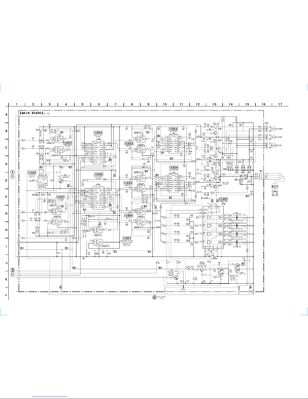
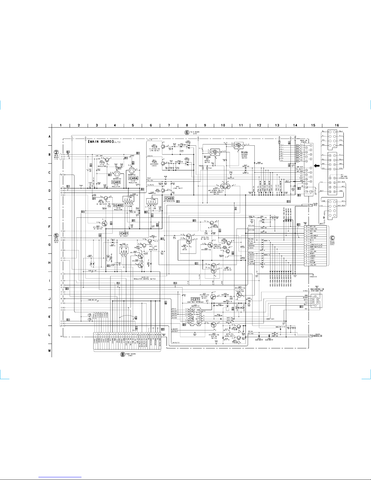
2-1. NOTE FOR PRINTED WIRING BOARDS AND SCHEMATIC DIAGRAMS
(In addition to this, the necessary note is printed in each block)
Caution:
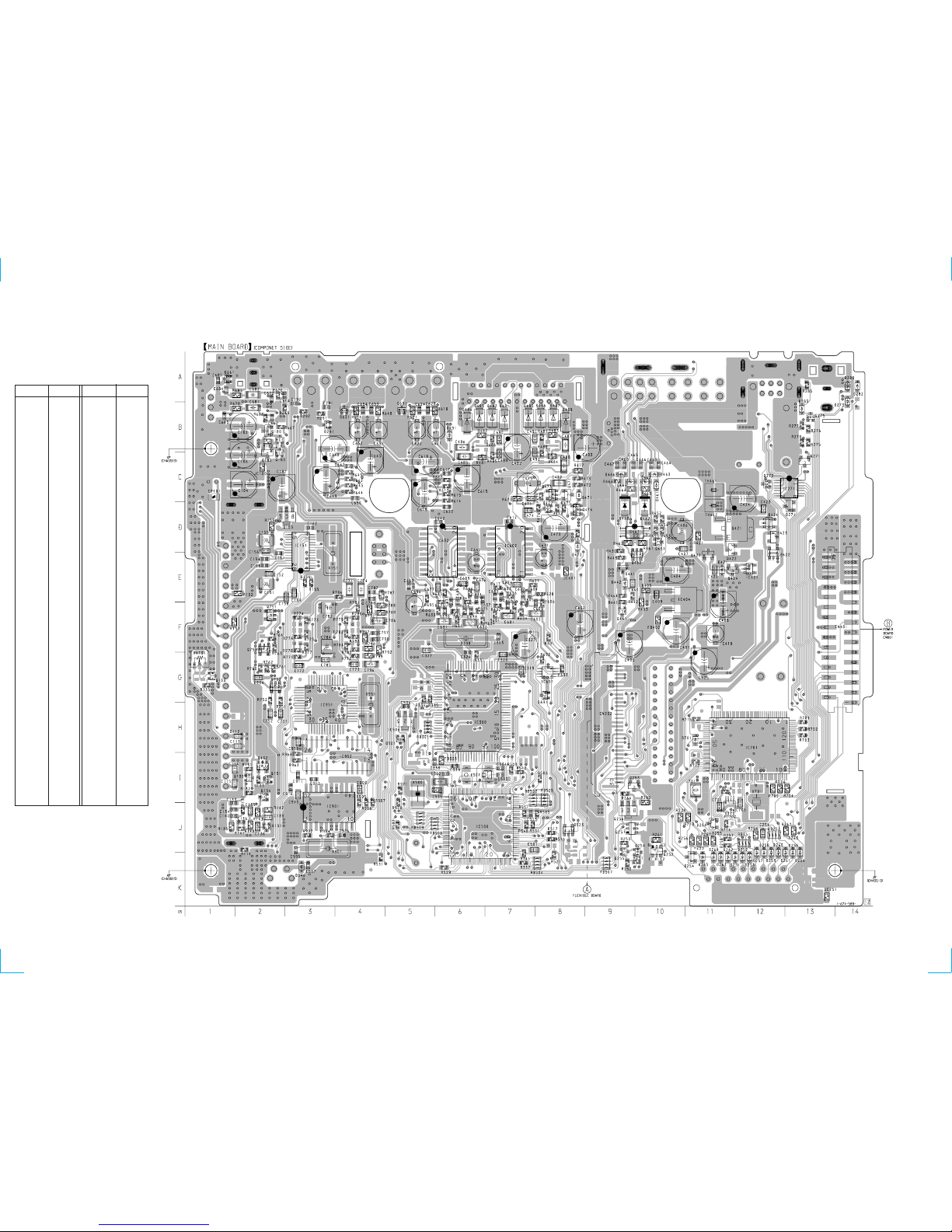
Pattern face side: Partsonthepattern facesideseen from
(Conductor Side) the pattern face are indicated.
Parts face side: Parts on the parts face side seen from
(Component Side) the parts face are indicated.
Note on PrintedWiring Boards:
•X: parts extracted from the component side.
•Y: parts extracted from the conductor side.
•f: internal component.
•b: Pattern from the side which enables seeing.
(The other layers' patterns are not indicated.)
Note on Schematic Diagrams:
• All capacitors are in µF unless otherwise noted. pF: µµF
50 WV or less are not indicated except for electrolytics
and tantalums.
• All resistors are in Ωand 1/4W or less unless otherwise
specified.
•f: internal component.
•C: panel designation.
•U: B+ Line.
•H: adjustment for repair.
• Powervoltageisdc14.4V andfedwithregulateddcpower
supply from ACC and BATT cords.
• Voltagesare takenwith aVOM(Input impedance10 MΩ).
Voltage variations may be noted due to normal produc-
tion tolerances.
• Waveforms are taken with a oscilloscope.
Voltage variations may be noted due to normal produc-
tion tolerances.
• Circled numbers refer to waveforms.
• Signal path.
F: FM
f: MW/LW
E: MD
• Model Identification
Thedestination is expressedwith the model according to
the language of Program Rom mounted in the set.
How to identify the model is described below.
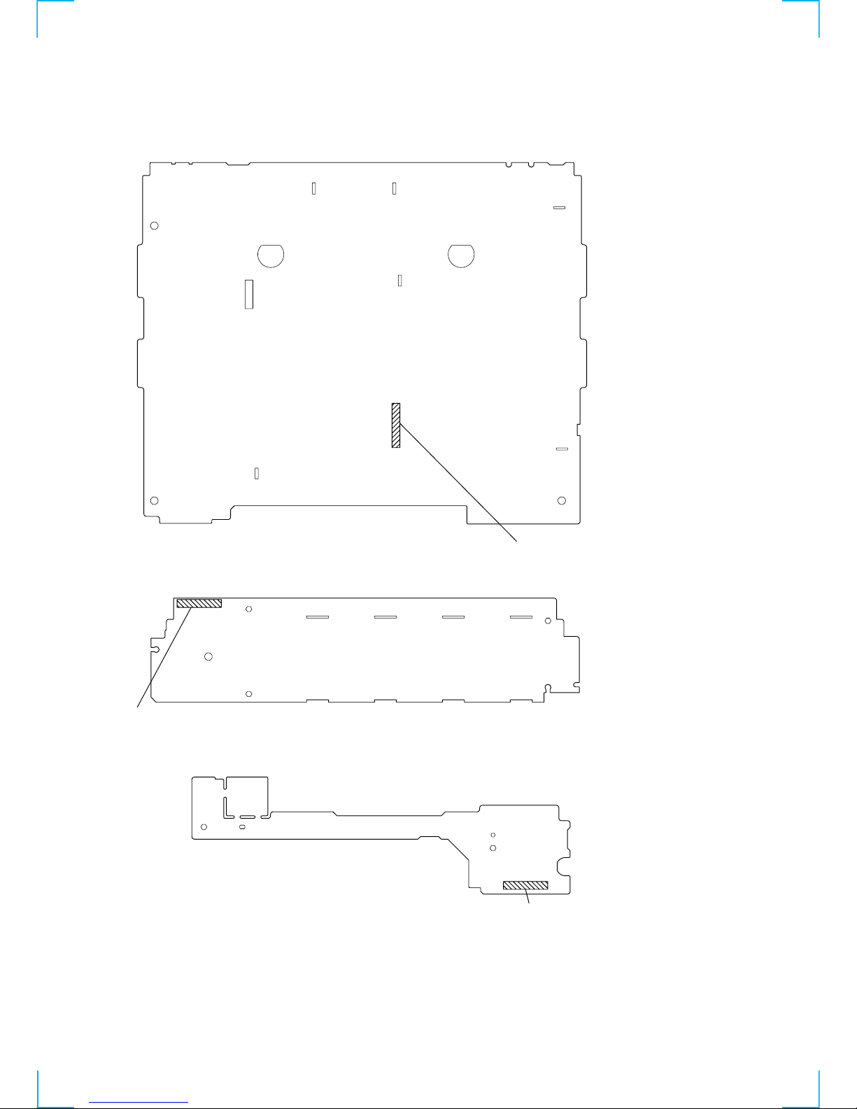
– POWER BOARD (Component Side) –
Note: The components identified by mark 0or dotted line
with mark 0are critical for safety.
Replace only with part number specified.