CRF-230B
Section
1.
TABLE
OF
CONTENTS
Section
Title
Page
OUTLINE?
coicccecueticecetecestchec
Piste
gteiees
peed
3
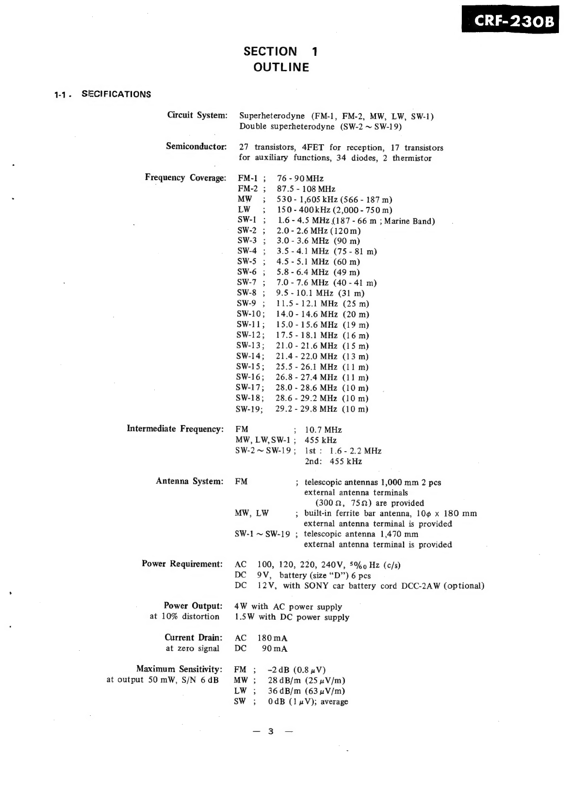
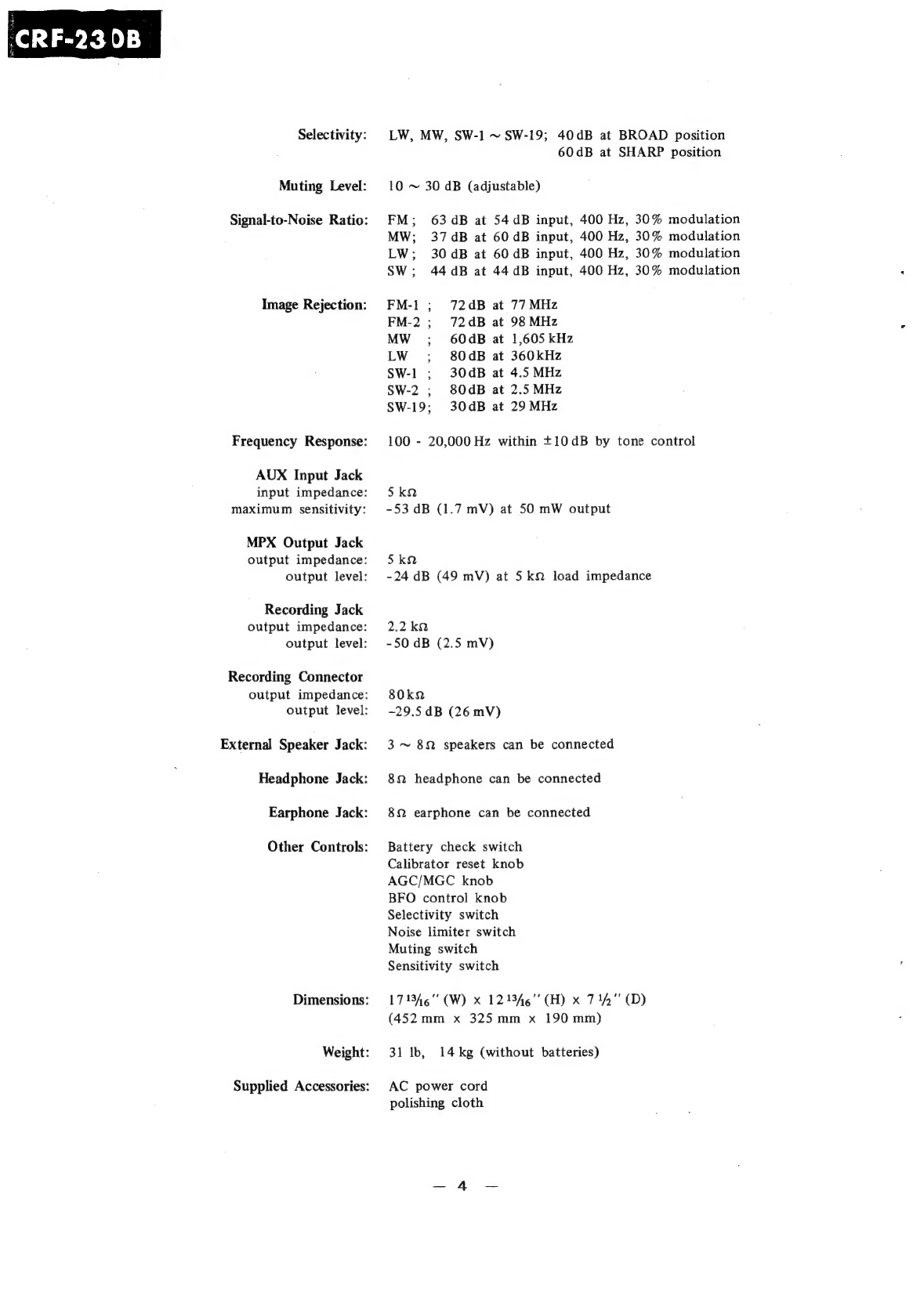
1-1.
Specifications
3
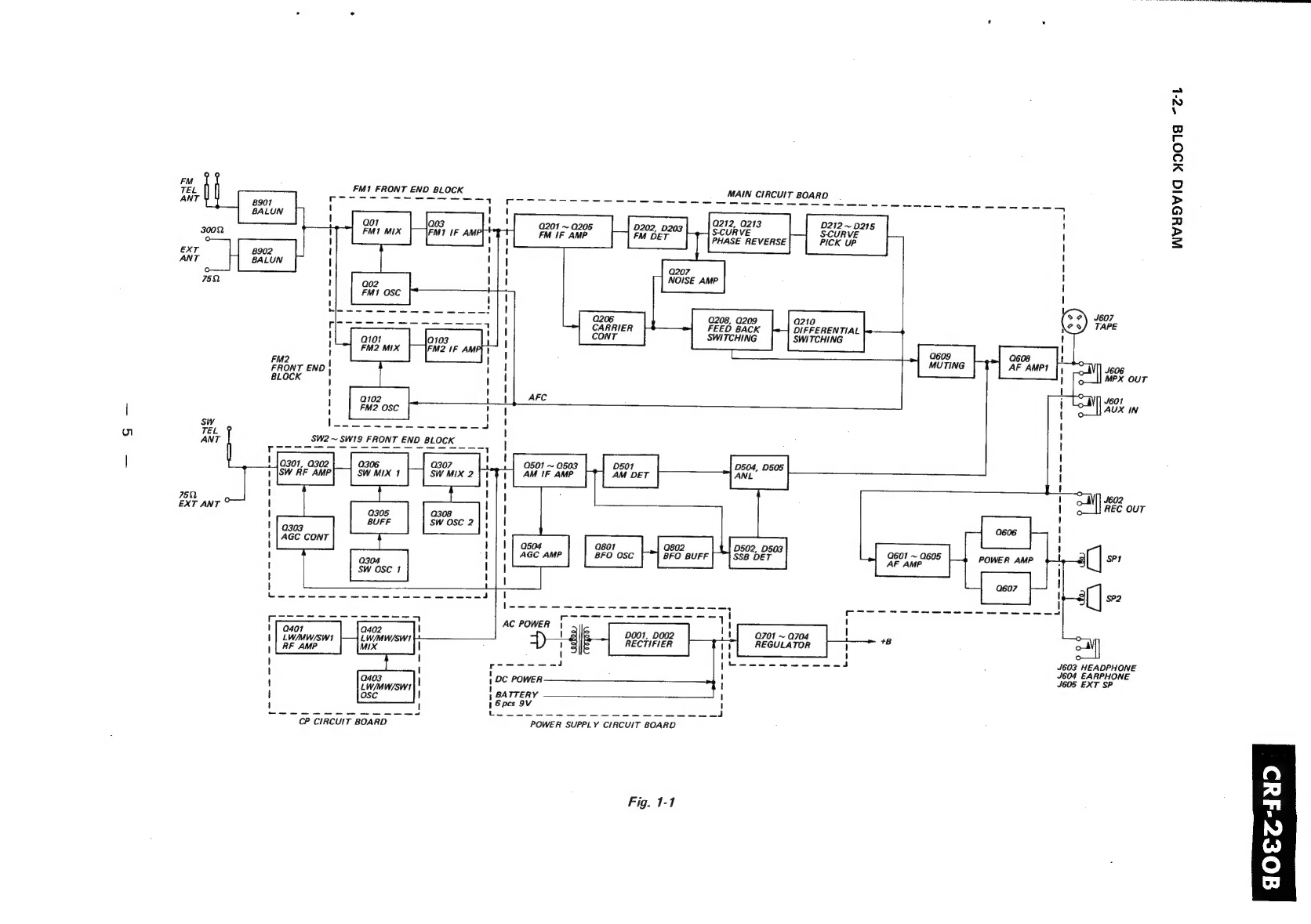
1-2.
Block
Diagram
2.0.0...
cece
ceeecceceeeeeeoeeee
5
1-3.
Technical
Features
.........ccccccsssccsseeeeees
6
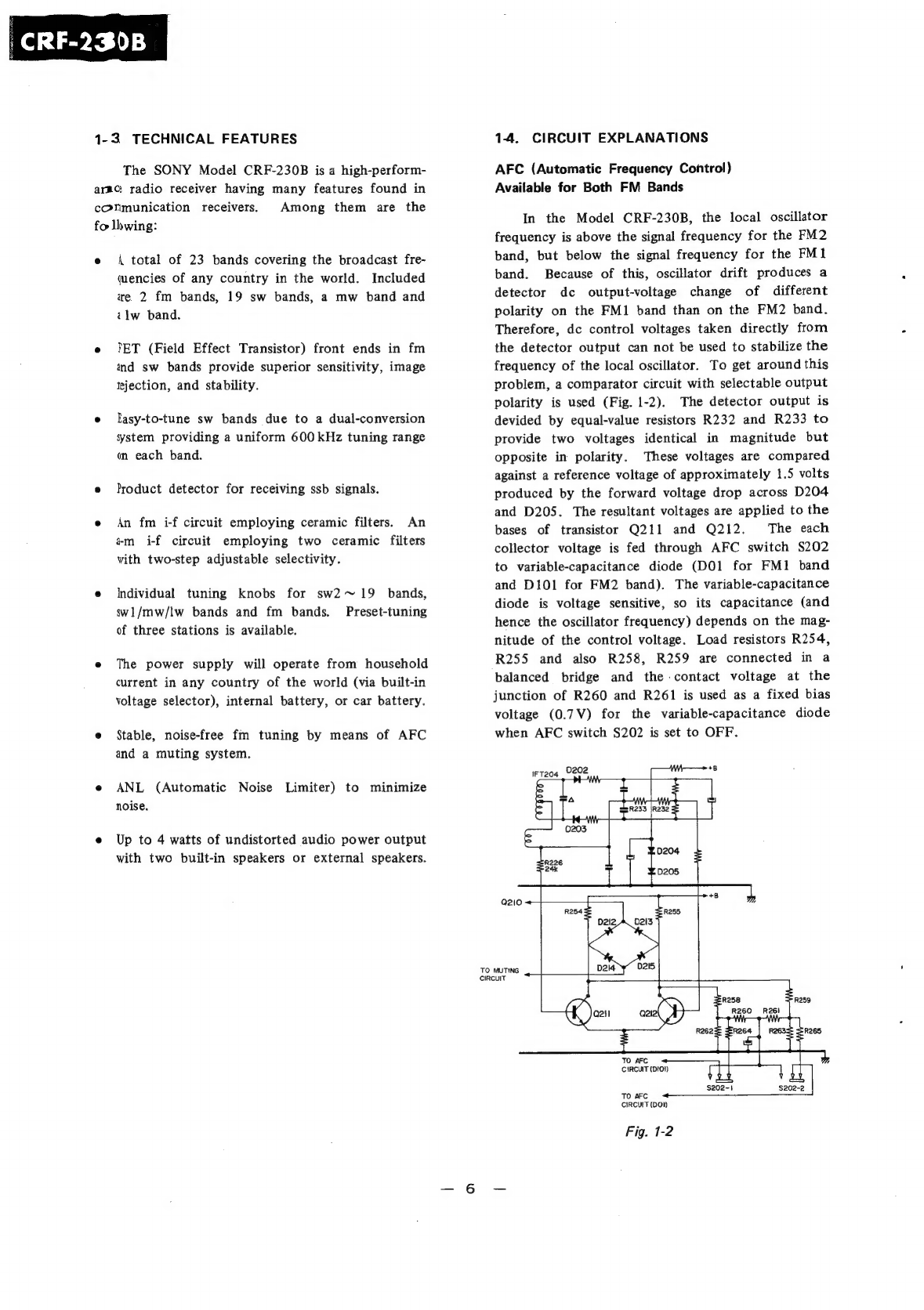
1-4,
Circuit
Explanations
.............cceeeeeeeeee
6
1-5...
External
“View
2..ceccc.ce.ciiscssuecacavesseneaee
10
1-6.
Internal
View
0.0...
eeesseetseeeeeeeneeeeee
10
V7...
Chassis:
View
ss.icetc.feqvegietssoseceaacstaeute
11
DISASSEMBLY
000...
ce
ceseeecesseeeeerseeeeee
12
2-1.
Rear
Cover
Removal
..........ccccceseeeeees
12
2-2.
Cabinet
Removal
.0.........cccceeeeseeteees
12
2-3.
Front
Panel
Removal
.............:ccceeeeee
13
2-4.
Speaker
Removal
.......ccceeeeeeeenseceeeeees
13
2-5.
Fm
Front
End
Block
Removal
.........
14
2-6.
Main
Circuit
Board
Removal
.............
14
2-7.
Sw
Front
End
Block
Removal
..........
15
2-8.
Cp
Circuit
Board
Removal
.......0..0..
15
2-9.
Power
Supply
Circuit
Board
Rei
OVal
ooo
yee
scsi
let
sctececivenetncsaesecs
16
2-10.
Dial
Cord
Stringing
......
eee
eeeeeeees
18
CIRCUIT
ADJUSTMENTS.
....00...
eee
20
3-1.
Preparation
00...
eee
3-2.
A-m
I-f
Alignment
3-3.
Ssb
Detector
Adjustment
.................
20
3-4.
Fm
I-f
Alignment
3-5.
Muting
Level
Setting
......
3-6.
FM1/FM2
Frequency
Coverage
and
Tracking
Adjustment
.............
22
3-7.
LW/MW/SW1
Frequency
Coverage
and
Tracking
Adjustment..............
24
Title
Page
3-8.
SW2~SW19
Ist
I-f
Alignment,
Frequency
Coverage
and
Tracking
Adjustment
..............0.06
25
3-9.
SW2~SWI19
Frequency
Coverage
and
Tracking
Adjustment
.............
26
3-10.
Voltage
and
Current
Adjustment
......
30
MOUNTING
AND
SCHEMATIC
DIAGRAMS
ooo
cece
cess
netceeeeeeeseeenes
32
4-1.
FM1
Front
End
(P1)
ou...
cee
eees
32
4-2.
FM2
Front
End
(P2)
........
cere
33
4-3.
Antenna
Terminal
(P3)
................0008
34
4-4,
Jack
Panel
(P4)
wo...
ecceeeeeeceee
sees
35
4-5.
Cp
Circuit
Board
(P5)
........ece
ee
eeeeeees
36
4-6.
Power
Supply
Circuit
Board
(P6)
.....
38
4-7.
SW2~SW19
Front
End
Block
(P7)
(SWC-011
D2)
ssccnciceceeietnie
dew
39
4-8.
Switch
Circuit
Board
(P9)
........0....
44
4-9.
Main
Circuit
Board
(P8)
..........
eee
45
4-10.
Schematic
Diagram
............cc.seeeeeeeeeen
47
PACKING
AND
EXPLODED
VIEW
..........
50
S21,
Packing
+.
2205.
kansinic
ie
etnies
50
5-2.
Exploded
View
(1)
......ccccceecesseeeeeeeeen
Sl
5-3.
Exploded
View
(2)
vo....cccceccceneeeeeeeen
53
5-4.
Exploded
View
(3)
........ccccecceseeeeereeen
55
5-5.
Exploded
View
(4)
.......c..cccceeeseeseeeeen
57
5-6.
Exploded
View
(5)
........cccceccesseeeeneeen
59
5-7.
Exploded
View
(6)
.......cccccccsseseeeeeeoen
61
ELECTRICAL
PARTS
LIST..............::0:0008
62