Sony HCD-RV990D User manual

1
Ver 1.3 2004. 09
DVD Model Name Using Similar Mechanism NEW
Section DVD Mechanism Type CDM74S-DVBU23
Optical Pick-up Name DBU-1
Tape Deck Model Name Using Similar Machanism HCD-RG550
Section Tape Transport Mechanism Type CWM43RR-23
SERVICE MANUAL
E Model
Australian Model
HCD-RV660D/RV990D
Amplifier section
The following measured at AC 120, 127, 220, 240 V,
50/60 Hz
Continuous RMS power output (reference)
Front speaker: 100 + 100 watts
(6 ohms at 1 kHz, 10%
THD)
Center speaker*: 40 watts (8 ohms at 1 kHz,
10% THD)
Surround speaker*: 40 + 40 watts
(6 ohms at 1 kHz, 10%
THD)
* MHC-RV990D only
Inputs
MD/VIDEO (AUDIO) IN (phono jacks):
voltage 450/250 mV,
impedance 47 kilohms
GAME (VIDEO) IN (phono jack):
1 Vp-p, 75 ohms
GAME (AUDIO) IN (phono jack):
voltage 250 mV,
impedance 47 kilohms
MIC (phone jack): sensitivity 1 mV,
impedance 10 kilohms
Outputs
MD/VIDEO (AUDIO) OUT (phono jacks):
voltage 250 mV,
impedance 1 kilohm
VIDEO OUT (phono jack):
max. output level
1 Vp-p, unbalanced, Sync
negative, load impedance
75 ohms
SPECIFICATIONS
S-VIDEO OUT (4-pin/mini-DIN jack):
Y: 1 Vp-p, unbalanced,
Sync negative,
C: 0.286 Vp-p, load
impedance 75 ohms
COMPONENT VIDEO OUT:
Y: 1 Vp-p, 75 ohms
PB, PR: 0.7 Vp-p, 75 ohms
PHONES (stereo mini jack):
accepts headphones of
8 ohms or more
Front speaker: Use only the supplied
speaker SS-RV990
Surround speaker (except for MHC-RV660D):
Use only the supplied
speaker SS-RS390
Center speaker (except for MHC-RV660D):
Use only the supplied
speaker SS-CT390
SUB WOOFER OUT: voltage 1 V,
impedance 1 kilohm
Sony Corporation
Audio Group
Published by Sony Engineering Corporation
9-961-078-04
2004I04-1
© 2004. 09
– Continued on next page –
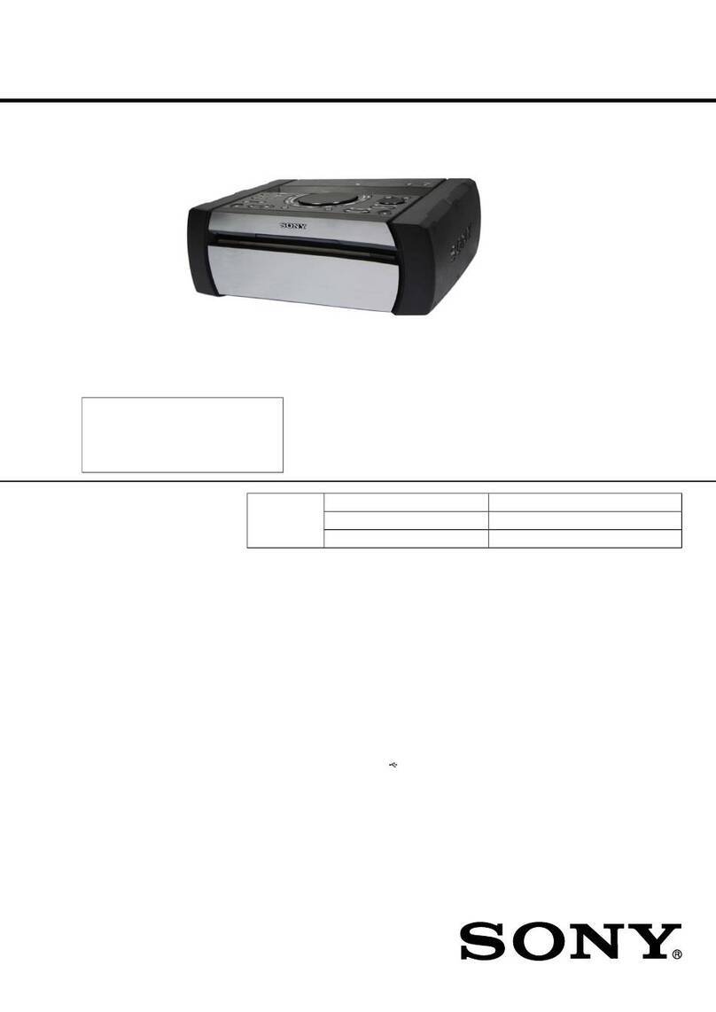
DVD DECK RECEIVER
•HCD-RV660D/RV990D are the
tuner, deck, DVD and amplifier
section in MHC-RV660D/RV990D. (Photo: HCD-RV990D)

2
HCD-RV660D/RV990D
SAFETY-RELATED COMPONENT WARNING!!
COMPONENTS IDENTIFIED BY MARK 0OR DOTTED LINE
WITH MARK 0ON THE SCHEMATIC DIAGRAMS AND IN
THE PARTS LIST ARE CRITICAL TO SAFE OPERATION.
REPLACE THESE COMPONENTS WITH SONY PARTS WHOSE
PART NUMBERS APPEAR AS SHOWN IN THIS MANUAL OR
IN SUPPLEMENTS PUBLISHED BY SONY.
Disc player section
System Compact disc and digital
audio and video system
Laser Semiconductor laser
(DVD: λ=650 nm,
CD: λ=780 nm)
Emission duration:
continuous
Frequency response DVD (PCM 48 kHz):
2 Hz – 22 kHz (±1 dB)
CD: 2 Hz – 20 kHz (±1 dB)
Video color system format
NTSC, PAL
OPTICAL DIGITAL OUT
(Square optical connector jack, rear panel)
Wavelength 660 nm
Tape deck section
Recording system 4-track 2-channel stereo
Frequency response 40 – 13,000 Hz (±3 dB),
using Sony TYPE I
cassette
Tuner section
FM stereo, FM/AM superheterodyne tuner
FM tuner section
Tuning range 87.5 – 108.0 MHz
Antenna FM lead antenna
Antenna terminals 75 ohm unbalanced
Intermediate frequency 10.7 MHz
AM tuner section
Tuning range
Latin American models: 530 – 1,710 kHz (with the
interval set at 10 kHz)
531 – 1,710 kHz (with the
interval set at 9 kHz)
Saudi Arabian model: 531 – 1,602 kHz (with the
interval set at 9 kHz)
Other models: 531 – 1,602 kHz (with the
interval set at 9 kHz)
530 – 1,710 kHz (with the
interval set at 10 kHz)
Antenna AM loop antenna
Antenna terminals External antenna terminal
Intermediate frequency 450 kHz
General
Power requirements
Australian model: 230 – 240 V AC, 50/60 Hz
Saudi Arabian model: 120 – 127 V, 220 V or
230 – 240 V AC,
50/60 Hz
Adjustable with voltage
selector
Mexican model: 127 VAC, 60 Hz
Thai model: 220 VAC, 50/60 Hz
Other models: 120 V, 220 V or 230 –
240 V AC, 50/60 Hz
Adjustable with voltage
selector
Power consumption
MHC-RV990D 300 watts
MHC-RV660D 230 watts
Dimensions (w/h/d) Approx. 280 ×325 ×368 mm
Mass
HCD-RV990D Approx. 12.1 kg
HCD-RV660D Approx. 10.6 kg
Design and specifications are subject to change without
notice.
Notes on Chip Component Replacement
•Never reuse a disconnected chip component.
•Notice that the minus side of a tantalum capacitor may be
damaged by heat.
Flexible Circuit Board Repairing
•Keep the temperature of soldering iron around 270°C during
repairing.
•Do not touch the soldering iron on the same conductor of the
circuit board (within 3 times).
•Be careful not to apply force on the conductor when soldering
or unsoldering.
UNLEADED SOLDER
Boards requiring use of unleaded solder are printed with the lead
free mark (LF) indicating the solder contains no lead.
(Caution: Some printed circuit boards may not come printed with
the lead free mark due to their particular size)
: LEAD FREE MARK
Unleaded solder has the following characteristics.
•Unleaded solder melts at a temperature about 40 °C higher than
ordinary solder.
Ordinary soldering irons can be used but the iron tip has to be
applied to the solder joint for a slightly longer time.
Soldering irons usinga temperatureregulator should beset toabout
350 °C.
Caution: The printed pattern (copper foil) may peel away if the
heated tip is applied for too long, so be careful!
•Strong viscosity
Unleaded solder is more viscou-s (sticky, less prone to flow) than
ordinary solder so use caution not to let solder bridges occur such
as on IC pins, etc.
•Usable with ordinary solder
It is best to use only unleaded solder but unleaded solder may also
be added to ordinary solder.
Ver 1.3
NOTE OF REPLACING THE DMB03 BOARD
When replacing the DMB03 board, since the adjustment value is
not set up correctly, “DriveAuto Adjustment” can’t be performed.
In this case, initialize Memory in the following procedures.
Procedure:
1. Set the test mode. (See supplement-1 page 4)
2. Press the [2] key of the remote commander, and set the “DRIVE
MANUAL OPERATION”. (See supplement-1 page 9)
3. Press the [6] key of the remote commander, and set the “2-6,
Memory Check”. (See supplement-1 page 11)
4. Press the [CLEAR] key of the remote commander, and initialize
Memory.
3
CAUTION
Use of controls or adjustments or performance of procedures
other than those specified herein may result in hazardous
radiation exposure.
HCD-RV660D/RV990D
NOTES ON HANDLING THE OPTICAL PICK-UP BLOCK
OR BASE UNIT
The laser diode in the optical pick-up block may suffer electrostatic
breakdown because of the potential difference generated by the
charged electrostatic load, etc. on clothing and the human body.
During repair, pay attention to electrostatic break-down and also
use the procedure in the printed matter which is included in the
repair parts.
The flexible board is easily damaged and should be handled with
care.
NOTES ON LASER DIODE EMISSION CHECK
The laser beam on this model is concentrated so as to be focused on
the disc reflective surface by the objective lens in the optical pick-
up block. Therefore, when checking the laser diode emission,
observe from more than 30 cm away from the objective lens.
Laser component in this product is capable
of emitting radiation exceeding the limit for
Class 1.
MODEL IDENTIFICATION
– BACK PANEL –
MODEL PARTS No.
RV990D: SP, MY 4-246-030-01
RV990D: E3, E15 4-246-030-11
RV990D: EA 4-246-030-21
RV990D: AUS 4-246-030-31
RV990D: E51 4-246-030-51
RV990D: MX 4-246-030-61
RV990D: PH 4-246-030-91
RV660D: SP, MY 4-246-139-01
RV660D: E3, E15 4-246-139-11
RV660D: EA 4-246-139-21
RV660D: AUS 4-246-139-31
RV660D: E51 4-246-139-51
RV660D: PH 4-246-139-61
RV660D: TH 4-250-550-41
RV990D: TH 4-250-557-41
•Abbreviation
E3 : 240 VAC area in E model
E15 : 220 – 240 VAC area in E model
E51 : 220 VAC area in E model
AUS : Australian model
EA : Saudi Arabia model
PH : Philippine model
SP : Singapore model
TH : Thai model
MY : Malaysia model
MX : Mexican model
SETTING AND RELEASING THE CD DISC TRAY LOCK
FUNCTION
This set has a disc tray lock function to prevent discs for
demonstration at shops from theft. While this lock function is set,
the tray will not be delivered out even when the OPEN/CLOSE
button is pressed.
Setting method:
Press the OPEN/CLOSE button while pressing the STOP button.
After a few seconds, the message “LOCKED” will appear on the
fluorescent indicator tube with the tray locked.
Releasing method:
Just as the lock is set, press the OPEN/CLOSE button while
pressing the STOP button.
After a few seconds, the message “UNLOCKED” will appear with
the lock released.
LASER DIODE AND FOCUS SEARCH OPERATION
CHECK
Carry out the “S curve check” in “DVD section adjustment” and
check that the S curve waveforms is output three times.
PARTS No.
This appliance is
claassified as a CLASS 1
LASER product. This
label is located on the
rear exterior.
The following caution label is located inside the apparatus.

4
TABLE OF CONTENTS
HCD-RV660D/RV990D
1. GENERAL
Main Unit ................................................................................ 5
Remote Control ....................................................................... 6
2. DISASSEMBLY
2-1. Case ..................................................................................... 8
2-2. CD Door .............................................................................. 8
2-3. Front Panel Section ............................................................. 9
2-4. DVD Block Section............................................................. 9
2-5. Tape Mechanism Deck ...................................................... 10
2-6. Panel Board, LED Board, Remote Board ......................... 10
2-7. Jack Board ......................................................................... 11
2-8. Back Panel Section............................................................ 11
2-9. Main Board (HCD-RV990D) ............................................ 12
2-10. Main Board (HCD-RV660D) ............................................ 12
2-11. Surround Board, Front AMP Board (HCD-RV990D)....... 13
2-12. DVD Mechanism Block, DMB03 Board, Video Board .... 13
2-13. Pick-up Unit ...................................................................... 14
2-14. SW Board, Driver Board ................................................... 14
2-15. Sensor Board ..................................................................... 15
2-16. Motor (TB) Board ............................................................. 15
2-17. Motor (LD) Board .............................................................16
3. DIAGRAMS
3-1. Circuit Boards Location .................................................... 17
3-2. Note for Printed Wiring Boards
and Schematic Diagrams .................................................. 17
3-3. Printed Wiring Board
–DVD Mechanism Section (1/2)– ..................................... 18
3-4. Schematic Diagram –DVD Mechanism Section (1/2)– .... 19
3-5. Printed Wiring Boards
–DVD Mechanism Section (2/2)– ..................................... 20
3-6. Schematic Diagram –DVD Mechanism Section (2/2)– .... 21
3-7. Printed Wiring Board –DMB03 Section– ......................... 22
3-8. Schematic Diagram –DMB03 Section (1/8)– ................... 24
3-9. Schematic Diagram –DMB03 Section (2/8)– ................... 25
3-10. Schematic Diagram –DMB03 Section (3/8)– ................... 26
3-11. Schematic Diagram –DMB03 Section (4/8)– ................... 27
3-12. Schematic Diagram –DMB03 Section (5/8)– ................... 28
3-13. Schematic Diagram –DMB03 Section (6/8)– ................... 29
3-14. Schematic Diagram –DMB03 Section (7/8)– ................... 30
3-15. Schematic Diagram –DMB03 Section (8/8)– ................... 31
3-16. Printed Wiring Board –Main Section– .............................. 32
3-17. Schematic Diagram –Main Section (1/4)– ........................ 33
3-18. Schematic Diagram –Main Section (2/4)– ........................ 34
3-19. Schematic Diagram –Main Section (3/4)– ........................ 35
3-20. Schematic Diagram –Main Section (4/4)– ........................ 36
3-21. Printed Wiring Board –Video Section– ............................. 37
3-22. Schematic Diagram –Video Section–................................ 38
3-23. Printed Wiring Board –Jack Section– ............................... 39
3-24. Schematic Diagram –Jack Section– ..................................40
3-25. Printed Wiring Board –FrontAMP Section– .................... 41
3-26. Schematic Diagram –FrontAMP Section– ....................... 42
3-27. Printed Wiring Boards –SurroundAMP Section– ............ 43
3-28. Schematic Diagram –Surround AMP Section–................. 44
3-29. Printed Wiring Boards –Panel Section– ............................ 45
3-30. Schematic Diagram –Panel Section– ................................ 46
3-31. Printed Wiring Board –Power Supply Section (1/2)– ....... 47
3-32. Schematic Diagram –Power Supply Section (1/2)– .......... 48
3-33. Printed Wiring Board –Power Supply Section (1/2)– ....... 49
3-34. Schematic Diagram –Power Supply Section (2/2)– .......... 50
3-35. IC Block Diagrams............................................................ 51
4. EXPLODED VIEWS
4-1. Main Section ..................................................................... 55
4-2. Front Panel Section (1)...................................................... 56
4-3. Front Panel Section (2)...................................................... 57
4-4. Front Panel Section (3)...................................................... 58
4-5. DVD Block Section........................................................... 59
4-6. Main Board Section (1/2).................................................. 60
4-7. Main Board Section (2/2).................................................. 61
4-8. DVD Mechanism Deck Section (1) .................................. 62
4-9. DVD Mechanism Deck Section (2) .................................. 63
5. ELECTRICAL PARTS LIST ........................................ 64

5
HCD-RV660D/RV990D
SECTION 1
GENERAL This section is extracted
from instruction manual.

6
HCD-RV660D/RV990D

7
HCD-RV660D/RV990D
SECTION 2
DISASSEMBLY
Note : Disassemble the unit in the order as shown below.
2-1. CASE
(Page 8)
2-2. CD DOOR
(Page 8)
SET
2-13. PICK-UP UNIT
(Page 14)
2-15. SENSOR BOARD
(Page 15)
2-16. MOTOR (TB) BOARD
(Page 15)
2-17. MOTOR (LD) BOARD
(Page 16)
2-14. SW BOARD,
DRIVER BOARD
(Page 14)
2-3. FRONT PANEL SECTION
(Page 9)
2-8. BACK PANEL SECTION
(Page 11)
2-9. MAIN BOARD (HCD-RV990D)
(Page 12)
2-10. MAIN BOARD (HCD-RV660D)
(Page 12)
2-11. SURROUND BOARD,
FRONT AMP BOARD
(HCD-RV990D)
(Page 13)
2-4. DVD BLOCK SECTION
(Page 9)
2-12. DVD MECHANISM BLOCK,
DMB03 BOARD,
VIDEO BOARD
(Page 13)
2-6. PANEL BOARD,
LED BOARD,
REMOTE BOARD
(Page 10)
2-5. TAPE MECHANISM DECK
(Page 10)
2-7. JACK BOARD
(Page 11)

8
HCD-RV660D/RV990D
2-2. CD DOOR
Note : Follow the disassembly procedure in the numerical order given.
2-1. CASE
1
two screws
(case 3 TP2)
2
screw
(case 3 TP2)
4
screw
(case 3 TP2)
3
two screws
(case 3 TP2)
5
four screws (+BVTT 3
×
6)
9
case
6
three screws
(+BVTT 3
×
6)
7
7
8
2
Pull-out the disc tray.
4
CD door
1
Turn the pulley to the direction of arrow.
pulley
Front panel side
CD mechanism deck (CDM74S-DVBU23)
3
Ver 1.1

9
HCD-RV660D/RV990D
2-3. FRONT PANEL SECTION
2-4. DVD BLOCK SECTION
6
CN501
9
CN605
qa
CN502
qd
CN503
8
CN70
6
7
CN304
0
connector
qs
connector
2
screw
(+BVTP 3
×
8)
3
screw
(+BVTP 3
×
8)
4
screw
(+BVTP 3
×
8)
5
lug
1
three screws (+BVTP 3
×
8)
qf
front panel section
2
three
screws
(+BVTT 3
×
6
)
1
three
screws
(+BVTP 3
×
8)
3
4
CN804
5
CN301
6
CN101
7
CN543
8
DVD block section
Ver 1.1

10
HCD-RV660D/RV990D
2-5. TAPE MECHANISM DECK
2-6. PANEL BOARD, LED BOARD, REMOTE BOARD
2
two
screws
(+BVTP 2.6
×
8)
4
two
screws
(+BVTP 2.6
×
8
)
3
three
screws
(+BVTP 2.6
×
8)
5
tape mechanism deck
1
connector
1
volume knob
8
PANEL board
0
LED board
qs
REMOTE board
7
two claws
qa
CN102
2
three
screws
(+BVTP 2.6
×
8)
3
two
screws
(+BVTP 2.6
×
8)
4
two
screws
(+BVTP 2.6
×
8
)
9
two
screws
(+BVTP 2.6
×
8)
6
two
screws
(+BVTP 2.6
×
8)
5
three
screws
(+BVTP 2.6
×
8)

11
HCD-RV660D/RV990D
2-8. BACK PANEL SECTION
2-7. JACK BOARD
1
two
screws
(+BVTP 2.6
×
8)
4
shield plate
6
JACK board
5
two mic knobs
2
screw
(+BVTT 3
×
6)
3
screw
(+BVTT 3
×
6)
qs
back panel section
5
four
screws
(+BVTT 3
×
6)
8
three
screws
(+BVTP 3
×
8)
6
screw
(+BVTP 3
×
8)
9
two
screws
(+BVTT 3
×
6)
7
two
screws
(+BVTP 3
×
8)
qa
CN704
0
1
CN917
3
CN901
4
CN902
2
CN102
Ver 1.1

12
HCD-RV660D/RV990D
2-9. MAIN BOARD (HCD-RV990D)
2-10. MAIN BOARD (HCD-RV660D)
7
two
screws
(+BVTP 3
×
6)
4
two
screws
(+BVTP 3
×
8)
qd
MAIN boar
d
5
screw
(+BVTT 3
×
6)
6
screw
(+BVTT 3
×
6)
8
screw
(+BVTT 3
×
6)
9
qs
two claws
SURROUND board
1
CN914
2
CN915
3
CN913
0
CN901
qa
CN303
7
two
screws
(+BVTP 3
×
6)
4
two
screws
(+BVTP 3
×
8)
qs
MAIN boar
d
5
screw
(+BVTT 3
×
6)
6
screw
(+BVTT 3
×
6)
8
screw
(+BVTT 3
×
6)
9
qa
claw
LEAD PIN board
CN707
CN705
1
CN914
2
CN915
3
CN913
0
CN303
Ver 1.1

13
HCD-RV660D/RV990D
2-12. DVD MECHANISM BLOCK, DMB03 BOARD, VIDEO BOARD
2-11. SURROUND BOARD, FRONT AMP BOARD (HCD-RV990D)
1
CN302
2
CN372
3
two
screws
(+BVTP 3
×
16)
4
two
screws
(+BVTP 3
×
1
6)
5
SURROUND board
6
FRONT AMP board
2
screw
(+BVTP 3
×
8
)
bracket (DVD)
7
two
screws
(+BVTT 3
×
6)
qa
two
screws
(+BVTP 3
×
8)
qs
VIDEO board
9
heat sink
0
DMB03 board
8
two
screws
(+BVTT 3
×
6)
4
3
screw
(+BVTP 3
×
8)
1
CN501
qd
DVD mechanism block
5
CN102
6
CN801
Ver 1.1

14
HCD-RV660D/RV990D
2-13. PICK-UP UNIT
2-14. SW BOARD, DRIVER BOARD
9
two insulators
0
insulator
5
RF board
2
two screws
(+BTP M2.6)
qa
pick-up unit
holder (DBU) assy
3
CN003
4
CN001
1
floating
screw
(+PTPWH M2.6
)
6
floating
screw
(+PTPWH M2.6)
7
floating
screw
(+PTPWH M2.6)
8
floating
screw
(+PTPWH M2.6)
6
DRIVER boar
d
2
SW board
3
CN704
4
CN703
7
CN702 (flat type)
5
two
screws
(+BTTP (M2.6))
1
screw
(+BTTP (M2.6))

15
HCD-RV660D/RV990D
2-16. MOTOR (TB) BOARD
2-15. SENSOR BOARD
2
tray
3
belt (table)
5
pulley (table)
8
screw
(+BTTP (M2.6))
9
SENSOR board
7
gear (geneva)
0
CN731
1
floating
screw
(+PTPWH M2.6)
6
floating
screw
(+PTPWH M2.6)
4
floating
screw
(+PTPWH M2.6)
4
Remove the two solderings of motor.
3
MOTOR (TB) board
5
table motor assy (M741)
2
two
screws
(+BTTP (M2.6))
1

16
HCD-RV660D/RV990D
2-17. MOTOR (LD) BOARD
4
Remove the two solderings of motor.
3
MOTOR (LD) board
1
belt (loading)
5
loading motor assy (M751)
2
two
screws
(+BTTP (M2.6))

17 17
HCD-RV660D/RV990D
3-2. NOTE FOR PRINTED WIRING BOARDS AND SCHEMATIC DIAGRAMS
Note on Printed Wiring Board:
•X: parts extracted from the component side.
•Y: parts extracted from the conductor side.
•: Pattern from the side which enables seeing.
(The other layer’s patterns are not indicated.)
Caution:
Pattern face side: Partsonthepatternface side seen from
(Conductor Side) the pattern face are indicated.
Parts face side: Parts on the parts face side seen from
(Component Side) the parts face are indicated.
C
BThese are omitted.
E
Q
B
These are omitted.
CE
Q
B
These are omitted.
CE
Q
Note on Schematic Diagram:
•All capacitors are in µF unless otherwise noted. pF: µµF
50 WV or less are not indicated except for electrolytics
and tantalums.
•All resistors are in Ωand 1/4W or less unless otherwise
specified.
•2: nonflammable resistor.
•C: panel designation.
•Indication of transistor. •A: B+ Line.
•B: B– Line.
•Voltage and waveforms are dc with respect to ground
under no-signal (detuned) conditions.
• TUNER/AUDIO section
no mark : no signal
• TAPE section
no mark : PLAY
():REC
• DVD section
no mark : STOP
():PLAY
∗: Impossible to measure
•Voltagesaretaken with a VOM (Input impedance10MΩ).
Voltage variations may be noted due to normal produc-
tion tolerances.
•Waveforms are taken with a oscilloscope.
Voltage variations may be noted due to normal produc-
tion tolerances.
•Circled numbers refer to waveforms.
•Signal path.
F: TUNER
L: VIDEO (COMPONENT)
r: VIDEO (COMPOSITE)
E: TAPE PLAY
a: TAPE REC
J: DVD (AUDIO)
c: DVD (RF)
I: DVD (DIGITAL)
• Abbreviation
E3 : 240 V AC area in E model
E15 : 220 – 240 VAC area in E model
E51 : 220 VAC area in E model
AUS : Australian model
EA : Saudi Arabia model
PH : Philippine model
SP : Singapore model
TH : Thai model
MY : Malaysia model
MX : Mexican model
Note: The components identified by mark 0or dotted line
with mark 0are critical for safety.
Replace only with part number specified.
UNLEADED SOLDER
Boards requiring use of unleaded solder are printed with the lead
free mark (LF) indicating the solder contains no lead.
(Caution: Some printed circuit boards may not come printed with
the lead free mark due to their particular size)
: LEAD FREE MARK
Unleaded solder has the following characteristics.
•Unleaded solder melts at a temperature about 40 °C higher than
ordinary solder.
Ordinary soldering irons can be used but the iron tip has to be
applied to the solder joint for a slightly longer time.
Soldering ironsusingatemperatureregulator should be set toabout
350 °C.
Caution: The printed pattern (copper foil) may peel away if the
heated tip is applied for too long, so be careful!
•Strong viscosity
Unleaded solder is more viscou-s (sticky, less prone to flow) than
ordinary solder so use caution not to let solder bridges occur such
as on IC pins, etc.
•Usable with ordinary solder
It is best to use only unleaded solder but unleaded solder may also
be added to ordinary solder.
3-1. CIRCUIT BOARDS LOCATION
SECTION 3
DIAGRAMS
MAIN board
DRIVER board
SW board
SUB TRANS board
DMB03 board
RF board
VIDEO board
MOTOR (LD) board MOTOR (TB) board
SENSOR board
TRANS board
FRONT AMP board
JACK board
PANEL board
SURROUND board
(HCD-RV990D)
LEAD PIN board
(HCD-RV660D)
REMOTE board
LED board

1818
HCD-RV660D/RV990D
• Refer to page 17 for Circuit Boards Location.
3-3. PRINTED WIRING BOARD — DVD MECHANISM SECTION (1/2) — • Refer to page 17 for Common Note on Printed Wiring Boards. : Uses unleaded solder.
Ref. No. Location
D001 C-11
D002 B-11
IC001 D-11
Q001 B-3
Q002 B-3
• Semiconductor
Location
(Page 22)
1
A
B
C
D
E
F
234567891011121314
DMB03
BOARD
CN501
A
1-684-822-
11
(11) 1-684-822-
11
(11)
R009
R008
R007
R005
R003
R004
C011
C010 Q001
Q002
CN001
C008
C009
C028 C027
C017
C015
C013
C049
CN002 C037
C038
C022
C041
C039
C040
C023
C021
C020
R016
R018
R012
R014
R001
CN003
R021
R015
R017
R011
R013
C042
C016
C019
D001
L001
D002
C004
C002 C006
C005
C001
C003
L002
R041
C018
R023 C024
C025
C030
R022
R026 C029 C031
R026
IC001
C032
R027
R010
R006
R028
R029
R032
C034 C033 C012
C035
R019
R020
R035
R033
C014
R025
R024
R036
R034
1
16
17 32
48
33
64 49
(SIDE A)
RF BOARD (SIDE B)
RF BOARD
OPTICAL PICK-UP
BLOCK
(DBU-1)

19 19
HCD-RV660D/RV990D
• Refer to page 17 for Common Note on Schematic Diagrams.
3-4. SCHEMATIC DIAGRAM — DVD MECHANISM SECTION (1/2) — • Refer to page 51 for IC Block Diagrams.
• Waveforms
– RF Board –
1
2
IC001 1(DVDRFP)
800mVp-p
3
4
IC001 el (TE)
IC001 r; (FE)
0.3Vp-p
1.3Vp-p
IC001 tj (RFAC)
0.5Vp-p
200mV/DIV, 100ns/DIV
500mV/DIV, 1ms/DIV
100mV/DIV, 1ms/DIV
500mV/DIV, 100ns/DIV
(Page 25)
IC B/D
JL005
C011
R033
C036 R034
C039
C038
C037
C040
R021
JL007
C003 R010R008R007
IOP1
L002
C004D002
R006
C001
C010
R004R003
IOP2
L001
C002D001
R022
R025
R023
C016
C015
C014
R014
R013
R012
R011
R018
R017
R016
R015
C042
C020
C021
C022
C023
R024
C027C028
C029
C018
C017
C019
C024
C031
C033 C012 C005
R032
JL003
JL006
R029
R028
R027
JL002
JL001
C032
C034
C049
C009
C035
CN003
CN001
CN002
C025
C006 C013
R005 R009
R035
R019 R020
C041
Q001 Q002
C008
R041
JL004
C030
C026
R001
(DBU-1)
R026
IC001

2020
HCD-RV660D/RV990D
• Refer to page 17 for Circuit Boards Location.
3-5. PRINTED WIRING BOARDS — DVD MECHANISM SECTION (2/2) — • Refer to page 17 for Common Note on Printed Wiring Boards. : Uses unleaded solder.
Ref. No. Location
D701 D-6
D711 D-7
IC701 F-6
IC712 F-7
IC731 D-11
Q731 B-8
• Semiconductor
Location
(Page 32)
1
A
B
C
D
E
F
G
H
23456789101112131415
OPEN/CLOSE
DETECT
DISC TRAY
ADDRESS
DETECT
CLOSE OPEN
CN751
S751
IC731
CN731
CN741
M741
CN742
C715
C731
C735
C736
R701
R711
R731
R721
R722
R723
R735
R732
R733
R734
D701
D711
Q731
C751
IC712
IC701
CN704
C737
R713
R712
C741
R702
JW702
JW703
JW704
JW705
JW706
JW707
JW708
JW711
CN703
CN702
CN705
R751
C752
CN701
JW712
JW701
JW709
JW710
JW713
JW714
RE701
CN721
M751
E3
E2
E1
This manual suits for next models
1
Table of contents
Other Sony Receiver manuals

Sony
Sony ICF-SW35 User manual

Sony
Sony DSX-M80 User manual

Sony
Sony XAV-701HD User manual

Sony
Sony 3-284-083-41(1) User manual

Sony
Sony STR-DN1070 User manual

Sony
Sony PWS-4400 User manual

Sony
Sony UWP-D11 User manual

Sony
Sony HCD-GZR88D User manual

Sony
Sony STR-DH700 User manual

Sony
Sony STR-DA5500ES User manual

Sony
Sony STR-DH550 User manual

Sony
Sony STR-DN610 User manual

Sony
Sony SAT-B2/2 User manual

Sony
Sony HBD-E370 User manual

Sony
Sony HWS-AV10K User manual

Sony
Sony STR-DB900 User manual

Sony
Sony STR-V5 User manual

Sony
Sony STR-VX500 User manual

Sony
Sony STR-DG500 - Multi Channel Av Receiver User manual

Sony
Sony HCD-HDX285 - Dvd Home Theater System User manual