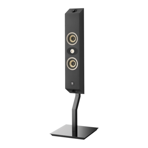
Sony SA-Z9R User manual

SERVICE MANUAL
Sony Video & Sound Products Inc.
ACTIVE REAR SPEAKER
9-896-494-01
2018B33-1
© 2018.02
US Model
Canadian Model
AEP Model
UK Model
Australian Model
Ver. 1.0 2018.02
• SA-Z9R other than the AUS model is an optional rear
speaker for exclusive HT-Z9F/ZF9.
• SA-Z9R of AUS model is a package rear speaker for
HT-Z9RF.
• Except AUS model
All of the units included in the right and left rear speak-
ers (SA-LZ9R/RZ9R) and the HT-Z9F (SA-Z9F/SA-
WZ9F/Remote control) or HT-ZF9 (SA-ZF9/SA-WZF9/
Remote control) are required to confirming operation of
this unit. Check in advance that you have all of the units.
• AUS model
All of the units included in the right and left rear speakers
(SA-LZ9R/RZ9R) and the HT-Z9RF (SA-Z9F/SA-WZ9F/
Remote control) are required to confirming operation of
this unit. Check in advance that you have all of the units.
SPECIFICATIONS
SA-Z9R
SA-LZ9R/RZ9R
Amplifier section
U.S. models:
POWER OUTPUT AND TOTAL HARMONIC DISTORTION:
(FTC)
With 4 ohms loads, both channels driven, from 200 -
20,000 Hz; rated 20 W per channel minimum RMS power,
with no more than 1% total harmonic distortion from
POWER OUTPUT (reference)
50 W (per channel at 4 ohms, 1 kHz)
Except US model:
POWER OUTPUT (rated)
30 W + 30 W (at 4 ohms, 1 kHz, 1% THD)
POWER OUTPUT (reference)
50 W (per channel at 4 ohms, 1 kHz)
Speaker system
Full range speaker system, Acoustic suspension
Speaker
46 mm (1 13/16 in) cone type, Full range speaker
Power requirements
120 V AC, 60 Hz (US, CND)
220 V - 240 V AC, 50 Hz/60 Hz (AEP, UK, AUS)
Power consumption
On: 11 W
Standby mode: 1 W or less
Turned o: 0.5 W or less
Dimensions (w/h/d) (approx.)
100 mm × 155 mm × 100 mm (4 in × 6 1/8 in × 4 in)
(projecting parts not included)
Mass (approx.)
1.0 kg (2lb 3 3/8 oz)
On copyrights
This product contains software that is subject to the
GNU General Public License (“GPL”) or GNU Lesser
General Public License (“LGPL”). These establish that
customers have the right to acquire, modify, and
redistribute the source code of said software in
accordance with the terms of the GPL or the LGPL.
For details of the GPL, LGPL and other software
licenses, please refer to [Software License
Information] under [Setup] - [Advanced Settings]
- [System Settings] on the product.
The source code for the software used in this product
is subject to the GPL and LGPL, and is available on
the Web. To download, please access the following:
URL:
http://oss.sony.net/Products/Linux
Please note that Sony cannot answer or respond to
any inquiries regarding the content of this source
code.
All other trademarks are trademarks of their
respective owners.
Wireless transmitter/receiver section
Communication system
Wireless Sound Specification Version 4.0
Frequency band
5 GHz
Modulation method
OFDM
Included items
• Rear speaker R (1), Rear speaker L (1)
• Operating Instructions (1)
Radio Frequency Bands and Maximum Output
Power
Frequency band Maximum output power
5150 - 5250 MHz < 18 dBm
5250 - 5350 MHz < 18 dBm
5470 - 5600 MHz < 18 dBm
5650 - 5725 MHz < 18 dBm
5725 - 5850 MHz < 13.98 dBm
Rear speaker L-ch SA-LZ9R
Rear speaker R-ch
SA-RZ9R
Photo: SA-LZ9R
(L-ch) Photo: SA-RZ9R
(R-ch)
COMPONENT MODEL NAME (SA-Z9R)

SA-Z9R
2
NOTES ON CHIP COMPONENT REPLACEMENT
• Never reuse a disconnected chip component.
• Notice that the minus side of a tantalum capacitor may be dam-
aged by heat.
SAFETY-RELATED COMPONENT WARNING!
COMPONENTS IDENTIFIED BY MARK 0OR DOTTED LINE
WITH MARK 0ON THE SCHEMATIC DIAGRAMS AND IN
THE PARTS LIST ARE CRITICAL TO SAFE OPERATION.
REPLACE THESE COMPONENTS WITH SONY PARTS
WHOSE PART NUMBERS APPEAR AS SHOWN IN THIS
MANUAL OR IN SUPPLEMENTS PUBLISHED BY SONY.
1. SERVICING NOTES ............................................. 3
2. DISASSEMBLY
2-1. Disassembly Flow........................................................... 6
2-2. Baffle Assy Block-1 ........................................................ 7
2-3. Baffle Assy Block-2 ........................................................ 8
2-4. Loudspeaker (46 mm)..................................................... 9
2-5. REAR JACK Board........................................................ 10
2-6. RF Modulator.................................................................. 11
2-7. SK2 REAR KEY Board.................................................. 12
2-8. Insulator Block................................................................ 13
2-9. Power-supply Cord ......................................................... 14
2-10. Insulator (S) .................................................................... 15
2-11. SK2 REAR MAIN Board ............................................... 16
2-12. Switching Regulator ....................................................... 17
3. TROUBLESHOOTING .......................................... 18
4. DIAGRAMS
4-1. Printed Wiring Board - SK2 REAR MAIN Board - ....... 23
4-2. Schematic Diagram
- SK2 REAR MAIN Board (1/2) -.................................. 24
4-3. Schematic Diagram
- SK2 REAR MAIN Board (2/2) -.................................. 25
4-4. Printed Wiring Board - REAR JACK Board - ................ 26
4-5. Schematic Diagram - REAR JACK Board -................... 26
5. EXPLODED VIEWS
5-1. Speaker Section............................................................... 29
5-2. Cabinet Section ............................................................... 30
5-3. SK2 REAR MAIN Board Section .................................. 31
6. ELECTRICAL PARTS LIST .............................. 32
Accessories are given in the last of the electrical parts list.
TABLE OF CONTENTS
SAFETY CHECK-OUT
After correcting the original service problem, perform the follow-
ing safety check before releasing the set to the customer:
Check the antenna terminals, metal trim, “metallized” knobs,
screws, and all other exposed metal parts for AC leakage.
Check leakage as described below.
LEAKAGE TEST
The AC leakage from any exposed metal part to earth ground and
from all exposed metal parts to any exposed metal part having a
return to chassis, must not exceed 0.5 mA (500 microamperes.).
Leakage current can be measured by any one of three methods.
1. A commercial leakage tester, such as the Simpson 229 or RCA
WT-540A. Follow the manufacturers’ instructions to use these
instruments.
2. A battery-operated AC milliammeter. The Data Precision 245
digital multimeter is suitable for this job.
3. Measuring the voltage drop across a resistor by means of a
VOM or battery-operated AC voltmeter. The “limit” indication
is 0.75 V, so analog meters must have an accurate low-voltage
scale. The Simpson 250 and Sanwa SH-63Trd are examples
of a passive VOM that is suitable. Nearly all battery operated
digital multimeters that have a 2 V AC range are suitable. (See
Fig. A)
1.5 kΩ0.15 μF
AC
voltmeter
(0.75 V)
To Exposed Metal
Parts on Set
Earth Ground
Fig. A. Using an AC voltmeter to check AC leakage.
ATTENTION AU COMPOSANT AYANT RAPPORT
À LA SÉCURITÉ!
LES COMPOSANTS IDENTIFIÉS PAR UNE MARQUE 0SUR
LES DIAGRAMMES SCHÉMATIQUES ET LA LISTE DES
PIÈCES SONT CRITIQUES POUR LA SÉCURITÉ DE FONC-
TIONNEMENT. NE REMPLACER CES COMPOSANTS QUE
PAR DES PIÈCES SONY DONT LES NUMÉROS SONT DON-
NÉS DANS CE MANUEL OU DANS LES SUPPLÉMENTS
PUBLIÉS PAR SONY.

SA-Z9R
3
SECTION 1
SERVICING NOTES
UNLEADED SOLDER
Boards requiring use of unleaded solder are printed with the lead-
free mark (LF) indicating the solder contains no lead.
(Caution: Some printed circuit boards may not come printed with
the lead free mark due to their particular size)
: LEAD FREE MARK
Unleaded solder has the following characteristics.
• Unleaded solder melts at a temperature about 40 °C higher
than ordinary solder.
Ordinary soldering irons can be used but the iron tip has to be
applied to the solder joint for a slightly longer time.
Soldering irons using a temperature regulator should be set to
about 350 °C.
Caution: The printed pattern (copper foil) may peel away if
the heated tip is applied for too long, so be careful!
• Strong viscosity
Unleaded solder is more viscous (sticky, less prone to flow)
than ordinary solder so use caution not to let solder bridges
occur such as on IC pins, etc.
• Usable with ordinary solder
It is best to use only unleaded solder but unleaded solder may
also be added to ordinary solder.
NOTE OF REPLACING THE FUSE
The fuse is or could be in the neutral. When a fuse is being re-
placed, the main plug shall be disconnected from the AC outlet to
prevent electric shock.
ADVANCE PREPARATION WHEN CONFIRMING OP-
ERATION
• Except AUS model
All of the units included in the right and left rear speakers (SA-
LZ9R/RZ9R) and the HT-Z9F (SA-Z9F/SA-WZ9F/Remote con-
trol) or HT-ZF9 (SA-ZF9/SA-WZF9/Remote control) are required
to confirming operation of this unit. Check in advance that you
have all of the units.
• AUS model
All of the units included in the right and left rear speakers (SA-
LZ9R/RZ9R) and the HT-Z9RF (SA-Z9F/SA-WZ9F/Remote con-
trol) are required to confirming operation of this unit. Check in
advance that you have all of the units.
NOTE OF PERFORMING THE OPERATION CHECK IN
THE STATE THAT HEAT SINK IS REMOVED
When performing the operation check in the state that this unit is
disassembled, it is possible to perform the operation check in the
state that heat sink is removed. However, don’t perform the opera-
tion check in the long time, and perform the operation check in the
volume state as low as possible.
ABOUT THE PROTECTION
If the power indicator on the rear speaker flashes in red, refer to
“ON/STANDBY indicator flashes in red (PROTECT)” on the
TROUBLESHOOTING (page 18).
The SERVICING NOTES contains important information for servicing. Be sure to read this section before repairing the unit.
MODEL IDENTIFICATION
Distinguish by Part No. and Destination code of the model number
label on the rear side of the main unit.
– Rear view –
US, CND
Except
US, CND
MODEL NUMBER LABEL
Destination code
Part No.
Model name
L/R channel discrimination
REAR L : for L-ch (SA-LZ9R)
REAR R : for R-ch (SA-RZ9R)
Destination code
Part No.
Model name
L/R channel discrimination
REAR L : for L-ch (SA-LZ9R)
REAR R : for R-ch (SA-RZ9R)
Model
name Part No. Destination
code Destination
SA-LZ9R
(L-ch)
4-728-510-0[] UC2 US, CND
4-728-512-0[] CEL AEP
4-728-513-0[] CEK UK
4-734-012-0[] AU1 AUS
SA-RZ9R
(R-ch)
4-728-510-1[] UC2 US, CND
4-728-512-1[] CEL AEP
4-728-513-1[] CEK UK
4-734-012-1[] AU1 AUS
DESTINATION ABBREVIATIONS
The following abbreviations for model destinations are used in this
service manual.
• Abbreviations
AEP : European area (Except for UK, Ireland), East European
area and CIS area (Moldova) models
AUS : Australian and New Zealand models
CND : Canadian and Latin American area (Puerto Rico) models
UK : European area (UK and Ireland) model

SA-Z9R
4
WIRELESS CONNECTION (LINK) WORK OF BAR SPEAK-
ER, SUBWOOFER AND REAR SPEAKERS
When the following parts are replaced, the wireless connection
(LINK) of the bar speaker and subwoofer/rear speakers will be
disconnected.
Before returning repaired products to the customer, be sure to refer
to the following, perform the work to LINK the bar speaker and
subwoofer or rear speakers.
Note 1: If only one unit of the bar speaker, subwoofer or rear speakers
is brought in for repair, wireless connection (LINK) is not pos-
sible. Refer to “What to do if only one unit of the bar speaker,
subwoofer or rear speakers are brought in for repair”.
Note 2: Rear speakers for except AUS model is optional product.
Rear speakers for AUS model is package product.
Replacing parts for repairing that required wireless con-
nection (LINK)
• Replacing the MAIN board of bar speaker
• Replacing the RF modulator of subwoofer
• Replacing the RF modulator of rear speakers
Wireless connection (LINK) method
After replacing the correspond parts of “Replacing parts for re-
pairing that required wireless connection (LINK)” above, wireless
connection will not automatically be done even if the power is
turned on.
Perform the work to follow the procedure below.
Procedure:
1. Connect bar speaker with TV monitor and press the [1] button
on the bar speaker to turn the power on.
2. Set the manual link of “Wireless Speaker Settings” from the
home menu.
Note 1: For the manual link setting procedure, please refer to “Manual
link setting method” below.
3. Confirm that the manual link between bar speaker and sub-
woofer or rear speakers was made.
Note 2: If can not manual linked, refer to “The subwoofer and rear speak-
ers are not linked” for “TROUBLESHOOTING” of service man-
ual of bar speaker (HT-Z9F/Z9RF/ZF9).
4. Reset the bar speaker, subwoofer and rear speakers.
Note 3: For the resetting procedure, please refer to “Resetting method” on
the right.
5. When returning the units to the customer, inform the each set-
ting is initialized by execute the reset.
Manual link setting method
Procedure:
1. Connect bar speaker with TV monitor.
2. Press the [1] button on the bar speaker to turn the power on.
3. Press the [1] button on the rear side of subwoofer and rear
speakers to turn the power on.
4. Press the [HOME] button on the remote control.
5. From the display of home menu on the TV monitor, operate
and decision in the following order.
“Setup” →“Advanced settings” →“Speaker settings” →
“Wireless Speaker Settings”→“Start manual linking”
6. Press the [LINK] button on the rear side of subwoofer and rear
speakers.
Note: Perform the next step within 2 minutes after the power on/standby
indicator is flashed.
7. From the display of home menu on the TV monitor, select the
“Start” and decision.
8. The message “Subwoofer : Connected”, “Rear Speaker (L) :
Connected” and “Rear Speaker (R) : Connected” are displayed
on the TV monitor.
9. Select the “Finish” →“Close”, the power on/standby indicator
of the subwoofer and rear speakers are lit in green and manual
link is completed.
Resetting method
• Bar speaker
Procedure:
1. Connect bar speaker with TV monitor and press the [1] button
on the bar speaker to turn the power on.
2. Press the [HOME] button on the remote control.
3. From the display of home menu on the TV monitor, operate
and decision in the following order.
“Setup” →“Advanced settings” →“Resetting” →“All set-
tings”→“Start”
Note 1: It can also reset by touch the two buttons of the [1] and [–] on the
bar speaker simultaneously for 5 seconds.
Note 2: Settings other than wireless connection settings will also be reset.
• Subwoofer or rear speakers
Procedure:
1. Press the [1] button for about 10 seconds on the rear side of
subwoofer and rear speakers.
Check the power on/standby indicator on the front side of the
subwoofer or the rear side of the rear speakers flashes alter-
nately green and orange.
– Subwoofer – – Rear speaker –
Power on/standby
indicator
Power on/standby
indicator
[1] button [1] button
2. Unplug the power cord of subwoofer and rear speakers from
the wall outlet.
What to do if only one unit of the bar speaker, subwoofer
or rear speakers are brought in for repair
If only one unit of the bar speaker, subwoofer or rear speakers
are brought in for repair situation, and the correspond parts of
“Replacing parts for repairing that required wireless connection
(LINK)” is replaced, the customer must need perform the wireless
connection (manual link) setting of the bar speaker and subwoofer
or rear speakers.
When returning the repaired product to the customer, be sure to in-
form the customer that it is necessary to set the wireless connection
(manual link) by referring to the Operating Instructions.
Note: In this case, wireless connection can not be made automatically.

SA-Z9R
5
NOTE OF REPLACING THE ELECTRICAL PARTS ON
EACH BOARDS FOR REPAIRING
Among mounted electrical parts on each boards, only parts that
are described in the electrical parts list can be replaced for repair.
The parts that are not described in the electrical parts list cannot be
replaced with single for repairing.
NOTE OF REPLACING THE SK2 REAR KEY BOARD
FOR REPAIRING
When the SK2 REAR KEY board is defective, replace the com-
plete mounted board.
The mounted parts cannot be replaced with single for repairing.
THE STRUCTURE OF SA-LZ9R (L-ch) AND SA-RZ9R
(R-ch)
The SA-LZ9R (L-ch) and SA-RZ9R (R-ch) are the same structure.
However, the model number label and the software written on the
RF modulator are different.
SPREADING OF COMPOUND
When the IC8010 on the SK2 REAR MAIN board or the SK2
REAR MAIN board is replaced, spread the compound to the
touching portion between the IC8010 and the heat sink.
– SK2 REAR MAIN Board (Side A) –
IC8010
compound

SA-Z9R
6
SECTION 2
DISASSEMBLY
• This set can be disassembled in the order shown below.
2-1. DISASSEMBLY FLOW
SET
2-2. BAFFLE ASSY BLOCK-1
(Page 7)
2-3. BAFFLE ASSY BLOCK-2
(Page 8)
2-6. RF MODULATOR
(Page 11)
2-7. SK2 REAR KEY BOARD
(Page 12)
2-8. INSULATOR BLOCK
(Page 13)
2-9. POWER-SUPPLY CORD
(Page 14)
2-10. INSULATOR (S)
(Page 15)
2-11. SK2 REAR MAIN BOARD
(Page 16)
2-12. SWITCHING REGULATOR
(Page 17)
2-4. LOUDSPEAKER (46 mm)
(Page 9)
2-5. REAR JACK BOARD
(Page 10)
Note: The SA-LZ9R (L-ch) and SA-RZ9R (R-ch) are the same structure.
However, the model number label and the software written on the
RF modulator are different.

SA-Z9R
7
Note: Follow the disassembly procedure in the numerical order given.
2-2. BAFFLE ASSY BLOCK-1
• Continued on 2-3 (page 8).
front side
right side
left side
+RZWRLQVWDOOWKHEDIIOHDVV\EORFN
rear side
6Remove the baffle assy
block in the direction
of the arrow.
4Pull out the baffle assy
block in the direction
of the arrow.
top side
front side
baffle assy block
left side
2Install the baffle assy block
in the direction of the arrow.
1three screws
(BVTP3.5 u10)
1three screws
(BVTP3.5 u10)
2two feet
3two screws
(BVTP3 u8)
7Draw out the leg from the
back of the screw hole on
the baffle assy.
screw
hole
screw
hole
leg
baffle assy block
cabinet block
1Insert the leg to the back of the
screw hole on the baffle assy.
cabinet block
leg
screw hole
rear side
Attach in order from 1to 4.
3Slide the baffle assy
block in the direction
of the arrow.
4Push in the baffle assy block
in the direction of the arrow.
5Slide the baffle assy
block in the direction
of the arrow.
baffle assy block

SA-Z9R
8
2-3. BAFFLE ASSY BLOCK-2
3 baffle assy block
2 terminal (narrow)
[black]
2 terminal (wide)
[red]
cabinet block
rear side
right side
left side
1Open the baffle assy block
in the direction of the arrow.
soft cloth, etc.
Note: When connecting the terminals of the speaker connection
cable to the loudspeaker, be careful of the direction of the
terminals.
,QVWDOODWLRQGLUHFWLRQIRUWKHWHUPLQDOV
top side
top side
speaker connection cable
loudspeaker
terminal (wide)
[red]
OK NG
OK NG
terminal (narrow)
[black]
bottom side

SA-Z9R
9
2-4. LOUDSPEAKER (46 mm)
right side
left side
soft cloth, etc.
– Inner view –
Note 2: When installing the loudspeaker (46 mm), make the
position of terminals as shown in the figure below.
,QVWDOODWLRQGLUHFWLRQIRUWKHORXGVSHDNHUPP
top side
bottom side
terminal
position
(narrow)
terminal
position
(wide)
top side
bottom side
1four screws
(BVTP3.5 u10)
2 loudspeaker (46 mm)
Note 1: When installing the loudspeaker,
align the two bosses and two holes.
baffle assy block
boss
boss
hole
hole
left
side
right
side

SA-Z9R
10
2-5. REAR JACK BOARD
3two screws
(BVTP3 u8)
4REAR JACK
board block
6Remove the REAR JACK board
in the direction of the arrow.
Turn over.
,QVWDOOLQJSRVLWLRQRIWKH5($5-$&.ERDUG
guide line REAR JACK board
rear side
5packing
(terminal)
7terminal case
8REAR JACK board
top side
front side right side
cabinet block
2harness (REAR-AMP~
REAR-JACK) connector
(CN8013)
1bushing
(terminal board)
+RZWRLQVWDOOWKHEXVKLQJWHUPLQDOERDUG
Attach in order from 1to 2.
2Push the bushing
(termianl board), to
fit inside the terminal
case as shown above
figure.
CN8013
termnal
case
harness (REAR-AMP
~REAR-JACK)
bushing (terminal board)
1Pinch the harness (REAR-AMP
~REAR-JACK) by the bushing
(termianl board), and insert
the bushing (termianl board)
to the terminal case.
top side
Check that the hole of jack and
connector are not covered by
the packing (terminal).
&KHFNDIWHULQVWDOOLQJWKH5($5
-$&.ERDUGEORFN
–5HDUYLHZ–
jack
packing
(terminal)
connector

SA-Z9R
11
2-6. RF MODULATOR
front side
right side
cabinet block
hole
1screw
(BVTP3 u8)
2
1screw
(BVTP3 u8)
4Draw out the FFC
block from the hole
of the stay block.
5screw
(BVTP3 u8)
5screw
(BVTP3 u8)
6stay block
7RF modulator
top side
FFC blcok
connector
3Unlock the connector.
terminal
side
front side
terminal
side
+RZWRLQVWDOOWKH))&EORFN
front side
Attach in order from 1to 5.
FFC block
RF modulator block
1Pass the FFC block through the
hole of the RF modulator block.
connector
2Lift up the lock plate
of the connector.
3Insert the FFC block
to the connector.
4Press down the lock plate
of the connector.
5Pull out the FFC
block downward.
hole
Note: When the RF modulator is replaced, be sure to refer to “WIRELESS CONNECTION
(LINK) WORK OF BAR SPEAKER, SUBWOOFER AND REAR SPEAKERS” on page 4.

SA-Z9R
12
2-7. SK2 REAR KEY BOARD
front side right side
cabinet block
hole
OK NG
The LED and two
buttons are not covered
by packing (key B).
The LED and two
buttons are covered
by packing (key B).
packing
(key B)
SK2 REAR KEY board SK2 REAR KEY board
packing
(key B)
boss
1screw
(BVTP3 u8)
3harness (REAR-AMP~
REAR-KEY) connector
(CN8001)
6packing (key B)
7SK2 REAR KEY board
Note: When installing the SK2 REAR KEY
board, align the boss and hole.
4cushion
5key block
top side
LED LED
button
button
button
button
3DVWLQJSRVLWLRQRIWKHSDFNLQJ.(<%
2

SA-Z9R
13
2-8. INSULATOR BLOCK
top side
+RZWRLQVWDOOWKHEXVKLQJWHUPLQDOERDUG
front side
right side
cabinet block
–6LGHYLHZ–
CN8013
bushing (terminal board)
2harness (REAR-AMP~
REAR-JACK) connector
(CN8013)
5power-supply cord
connector (CN1)
1bushing
(terminal board)
3screw
(BVTP3 u8)
3screw
(BVTP3 u8)
6insulator block
termnal
case
harness (REAR-AMP
~REAR-JACK)
Attach in order from 1to 2.
1Pinch the harness (REAR-AMP
~REAR-JACK) by the bushing
(termianl board), and insert
the bushing (termianl board)
to the terminal case.
2Push the bushing
(terminal board), to
fit inside the terminal
case as shown above
figure.
insulator
block
+RZWRLQVWDOOWKHLQVXODWRUEORFN
bush case
front side rear side
Insert the protrusion of the
insulator block to the back
of the bush case.
4Remove the insulator block in
the direction of the arrow.
claw side

SA-Z9R
14
2-9. POWER-SUPPLY CORD
right side
top side
claw side
left side
8power-supply
cord
power-supply cord
cord bushing (FBS001)
lock side
to switching regulator
5Draw out the power-supply
cord block from the hole.
,QVWDOODWLRQSRVLWLRQRIWKHFRUGEXVKLQJ)%6
80
+5, -0 mm
7cord bushing
(FBS001)
(See Fig. B)
6Unlock.
claw side
cabinet block
front side
hole
packing (bushing)
1screw
(BVTP3 u8)
1screw
(BVTP3 u8)
2bush case
Note: When installing the bush case, align
the two bosses and two holes.
3bushing (AC cable)
(See Fig. A)
boss
boss
hole hole
+RZWRLQVWDOOWKHEXVKLQJ$&FDEOH
bushing (AC cable)
Attach in order from 1to 2.
1Pinch the power-supply cord
block by the bushing (AC cable),
and insert the bushing (AC cable)
to the bush case.
2Push the bushing (AC cable),
to fit inside the bush case
as shown figure below.
bush case
power-supply cord block
)LJ$!
Push.
lock side
cord bushing (FBS001)
–,QQHUYLHZ–
top side
–5HDUYLHZ–
,QVWDOODWLRQGLUHFWLRQIRUWKHFRUGEXVKLQJ)%6
)LJ%!
cord bushing
(FBS001)
4claw
4claw

SA-Z9R
15
2-10. INSULATOR (S)
+RZWRLQVWDOOWKHLQVXODWRU6
front side
rear side
top side
left side
right side
1harness
(REAR-AMP~
REAR-KEY)
connector
(CN8026)
2harness
(REAR-AMP~
REAR-JACK)
connector
(CN8031)
3four screws
(BVTP3 u8)
4Draw out the FFC
block from the hole
of the insulator (S).
5insulator (S)
&KHFNDIWHULQVWDOOLQJ
WKHLQVXODWRU6
–7RSYLHZ–
Check that the holes of two
connectors are not covered
by the packing (main).
packing
(main)
insulator
(S)
connector
(CN8031)
connector
(CN8026)
chassis block
insulator block
speaker
connection cable
Attach in order from 1to 6.
1Position the speaker connection
cable in the direction of the arrow.
6Push the insulator (S) downward.
5Draw out the FFC block.
rear side
hole
hole
insulator (S)
3Pass the FFC block through
the hole of the insulator (S).
2Press.
rear side
4

SA-Z9R
16
2-11. SK2 REAR MAIN BOARD
:LUHVHWWLQJ
CN8025
top side
MAIN board
NG
The harness (SMPS~REAR-AMP)
is folded in the direction of the
arrow below.
–5LJKWYLHZ–
front side
rear side
top side
left side
right side
Press.
Press.
1speaker
connection
cable
connector
(CN8009)
2harness
(SMPS~REAR-AMP)
connector
(CN8025)
Attach in order from 1to 3.
1Fold the harness (SMPS~REAR-AMP)
in the direction of the arrow.
2Fold the harness (SMPS~REAR-AMP)
in the direction of the arrow.
3Press.
+RZWRLQVWDOOWKHSDFNLQJ
PDLQ
left side
3Unlock the connector (CN8022).
5absorbent (FFC) (short)
(Refer to “Processing method when
replacing the FFC (REAR-AMP~
WSMODULE) (50P)” )
terminal side
When replacing the FFC (REAR-AMP~WSMODULE) (50P)
to a new part, according to the step 1 to 3 figure below,
process the FFC (REAR-AMP~WSMODULE) (50P).
5absorbent (FFC) (long)
(Refer to “Processing method when
replacing the FFC (REAR-AMP~
WSMODULE) (50P)” )
6FFC (REAR-AMP~WSMODULE) (50P)
(Refer to “Processing method when
replacing the FFC (REAR-AMP~WSMODULE) (50P)” )
7punching (main)
8two screws
(BVTP3 u8)
9heat sink (main)
notch
notch
rib
rib
q; SK2 REAR MAIN board
Note 2: When installing the SK2 REAR
MAIN board, align the two ribs
and two notches.
4Draw out FFC block
from the connector
(CN8022).
FFC block
connector (
CN8022
)
terminal side
front side
no word side
3URFHVVLQJPHWKRGZKHQUHSODFLQJWKH
))&5($5$03a:602'8/(3
absorbent (FFC) (long)
Turn over.
38 mm
38 mm
1Paste absorbent
(FFC) (long) on the
no word side of the
FFC, and turn over it.
2Paste absorbent
(FFC) (short) on the
word side of the FFC
with aligning to
the guide line.
3Bend at the position
38 mm from both
ends of the FFC,
and crease it.
Note 3: Be sure to paste absorbent (FFC) (long)
on the no word side of the FFC.
absorbent
(FFC) (short)
word side
guide line
Note 1: When the SK2 REAR MAIN board is replaced, spread the compound
to the touching portion between the IC8010 and the heat sink.

SA-Z9R
17
2-12. SWITCHING REGULATOR
1SK2 REAR MAIN
cable connector
(CN101)
2two screws
(BVTP3 u8) 2two screws
(BVTP3 u8)
4claw
notch
hole
notch
rib
rib
5insulator
3chassis block
6switching regulator
Note: When installing the switching
regulator, align the two ribs
and two notches.
bottom side
top side
left side
front side
right side

SA-Z9R
18
SECTION 3
TROUBLESHOOTING
1. ON/STANDBY indicator flashes in red (PROTECT)
ON/STANDBY indicator flashes in
red.
(PROTECT)
IC8010 on the SK2 REAR MAIN
board is burned out.
ON/STANDBY indicator remains
flashing in red, when removing the
speaker connection connector
(CN8009) on the SK2 REAR MAIN
board and turning the power on.
Yes
Yes
Yes
No No
No
Check the speaker cable.
Check and replace the speaker
(SP1).
No
Check the mounted state of area surrounding IC8010 and
transistor (Q8008, Q8009) on the SK2 REAR MAIN board do
not short-circuits or opens. If there is no abnormality, IC8010
on the SK2 REAR MAIN board might have been damaged.
Replace the IC8010 on the SK2 REAR MAIN board.
Yes
Yes
The voltage of the following is 12 V.
SK2 REAR MAIN board:
IC8012 pin 4
Replace the IC8010 on the SK2
REAR MAIN board.
Yes
Replace the SK2 REAR MAIN
board.
(IC8012 on the SK2 REAR MAIN
board might have been damaged)
Replace the fuse (F8003) on the SK2 REAR
MAIN board. After the fuse replacing, if
immediately the fuse is damaging, IC8010
on the SK2 REAR MAIN board might have
been damaged. Replace the IC8010 on the
SK2 REAR MAIN board.
Fuse (F8003) on the SK2 REAR
MAIN board conduct the electricity.
No
Coil (L8001) on the SK2 REAR
MAIN board conduct the electricity.
Replace the SK2 REAR MAIN
board.
Resistor (R8287) on the SK2 REAR
MAIN board conduct the electricity.
Yes
No
Replace the resistor (R8287) on the
SK2 REAR MAIN board.
Note: The SA-LZ9R (L-ch) and SA-RZ9R (R-ch) are the same structure.
However, the model number label and the software written on the RF
modulator are different.

SA-Z9R
19
2. ON/STANDBY indicator does not light up (Power is not turned on)
– Switching regulator
(Conductor Side) –
ON/STANDBY indicator does not
light up.
(Power is not turned on)
The voltage of the following is about
21 V.
Switching regulator:
CN101 pin 1 to 3 (refer to Fig. A)
The voltage of the following is 4 V.
SK2 REAR MAIN board:
CN8022 pin 1 to 4
Yes
Switching regulator might have been
damaged. Replace the switching
regulator.
No
No Check the pattern of area surrounding connector (CN8022) on
the SK2 REAR MAIN board and POWER4V line. If there is no
abnormality, replace the RF modulator.
The AC-CUT signal is inputted to
pin 28 of connector (CN8022) on
the SK2 REAR MAIN board after
AC input.
Check the mounted state of area
surrounding IC8016 on the SK2
REAR MAIN board, and repair it.
No
The voltage of the following is 4 V.
SK2 REAR MAIN board:
IC8015 pin 3
Yes
No No
Check the area surrounding connector (CN8022) on the SK2
REAR MAIN board. If there is no abnormality, the RF modulator
or SK2 REAR MAIN board are abnormality. Replace the RF
modulator or SK2 REAR MAIN board.
Resistor (R8299) on the SK2 REAR
MAIN board conduct the electricity.
Replace the resistor (R8299) on the
SK2 REAR MAIN board.
Check the mounted state of area surrounding IC8015 on the
SK2 REAR MAIN board do not short-circuits or opens. If there
is no abnormality, IC8015 on the SK2 REAR MAIN board might
have been damaged.
Replace the IC8015 on the SK2 REAR MAIN board.
Yes
Yes
Yes
– Fig. A –
CN101 pin 1 to 3
Yes

SA-Z9R
20
3. The sound is not outputted
The waveform of the following is normal.
SK2 REAR MAIN board: IC8006
pin 11 (XTI), pin 55 (LRCKI),
pin 56 (BCKI), pin 1 (SDIN1)
Yes
The sound is outputted from the
connector (CN8009) on the SK2 REAR
MAIN board.
No
Check the area surrounding IC8006, vibrator (X001)
and connector (CN8022) on the SK2 REAR MAIN board.
Check the flexible flat cable (FFC1) (between RF
modulator and CN8022).
If there is no abnormality, replace the RF modulator or
flexible flat cable (FFC1).
Check the LC circuit of
amplifier output.
(L8019, L8020, C8063, and
C8064 on the SK2 REAR
MAIN board)
Yes
Yes
No
The sound is not outputted.
The waveform is outputted from the
IC8010 pin 35 (OUT_B), 39 (OUT_A), 40
(OUT_A) on the SK2 REAR MAIN board.
Yes
Yes
The waveform is outputted
from the IC8006 pin 16
(PWMOUT1PL), pin 17
(PWMOUT1NL) on the SK2
REAR MAIN board.
No
The reset signal inputted to
pin 4 of IC8010 on the SK2
REAR MAIN board from pin
40 of CN8022 on the SK2
REAR MAIN board.
No
Check the area surrounding IC8010 and
connector (CN8022) on the SK2 REAR
MAIN board.
Check the flexible flat cable (FFC1)
(between RF modulator and CN8022).
If there is no abnormality, replace the RF
modulator or flexible flat cable (FFC1).
No
The voltage of the following is 3.3 V.
SK2 REAR MAIN board: IC8006
pin 18 (VDDPWM1), pin 24 (VDDPWM2),
pin 30 (AVDD2R), pin 35 (AVDD2L),
pin 36 (AVDD1R), pin 41 (AVDD1L),
pin 47 (AVDDAD), pin 54 (DVDD)
Yes
Yes
Check the contact between connector
(CN8009) on the SK2 REAR MAIN
board and speaker cable.
Check the contact between speaker
(SP1) and speaker cable.
Yes
Check the mounted state of area surrounding
IC8010 on the SK2 REAR MAIN board do not
short-circuits or opens. If there is no
abnormality, IC8010 on the SK2 REAR MAIN
board might have been damaged. Replace
the IC8010 on the SK2 REAR MAIN board.
The waveform of the following is normal.
SK2 REAR MAIN board: IC8006
pin 12 (SCL), pin 13 (SDA),
pin 14 (XRESET), pin 15 (XINT)
No
Check the area surrounding connector
(CN8022) on the SK2 REAR MAIN board.
Check the flexible flat cable (FFC1)
(between RF modulator and CN8022).
If there is no abnormality, replace the RF
modulator or flexible flat cable (FFC1).
Check the mounted state of area
surrounding IC8006 on the SK2 REAR
MAIN board do not short-circuits or
opens. If there is no abnormality, IC8006
on the SK2 REAR MAIN board might
have been damaged. Replace the SK2
REAR MAIN board.
Yes
No
The voltage of the following is 3.3 V.
SK2 REAR MAIN board: IC8014 pin 3
Resistor (R8212) and coil (L8007, L8013)
on the SK2 REAR MAIN board conduct
the electricity.
Check again the area surrounding
IC8006 on the SK2 REAR MAIN board.
If there is no abnormality, replace the
SK2 REAR MAIN board.
Check again the area surrounding
IC8014 on the SK2 REAR MAIN board.
If there is no abnormality, replace the
IC8014 on the SK2 REAR MAIN board.
No
Replace the SK2 REAR MAIN board.
No
Yes
This manual suits for next models
2
Table of contents
Other Sony Speakers manuals