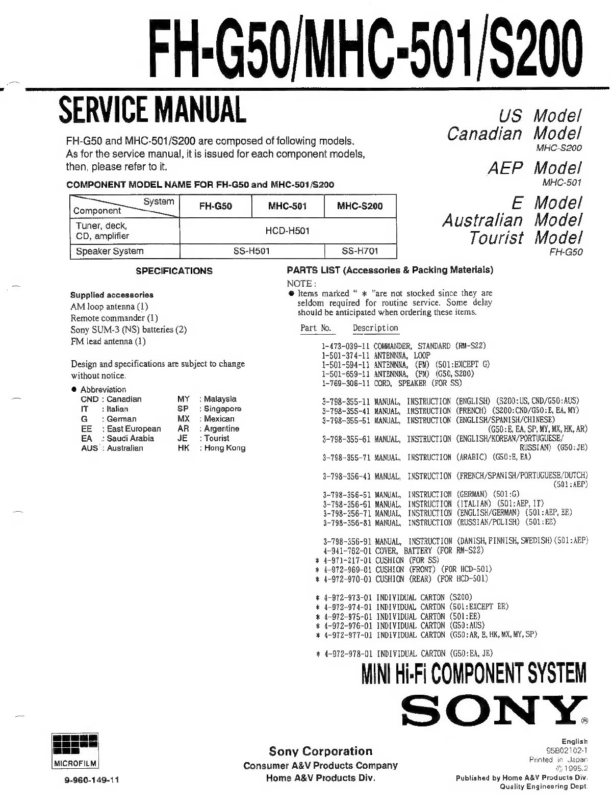
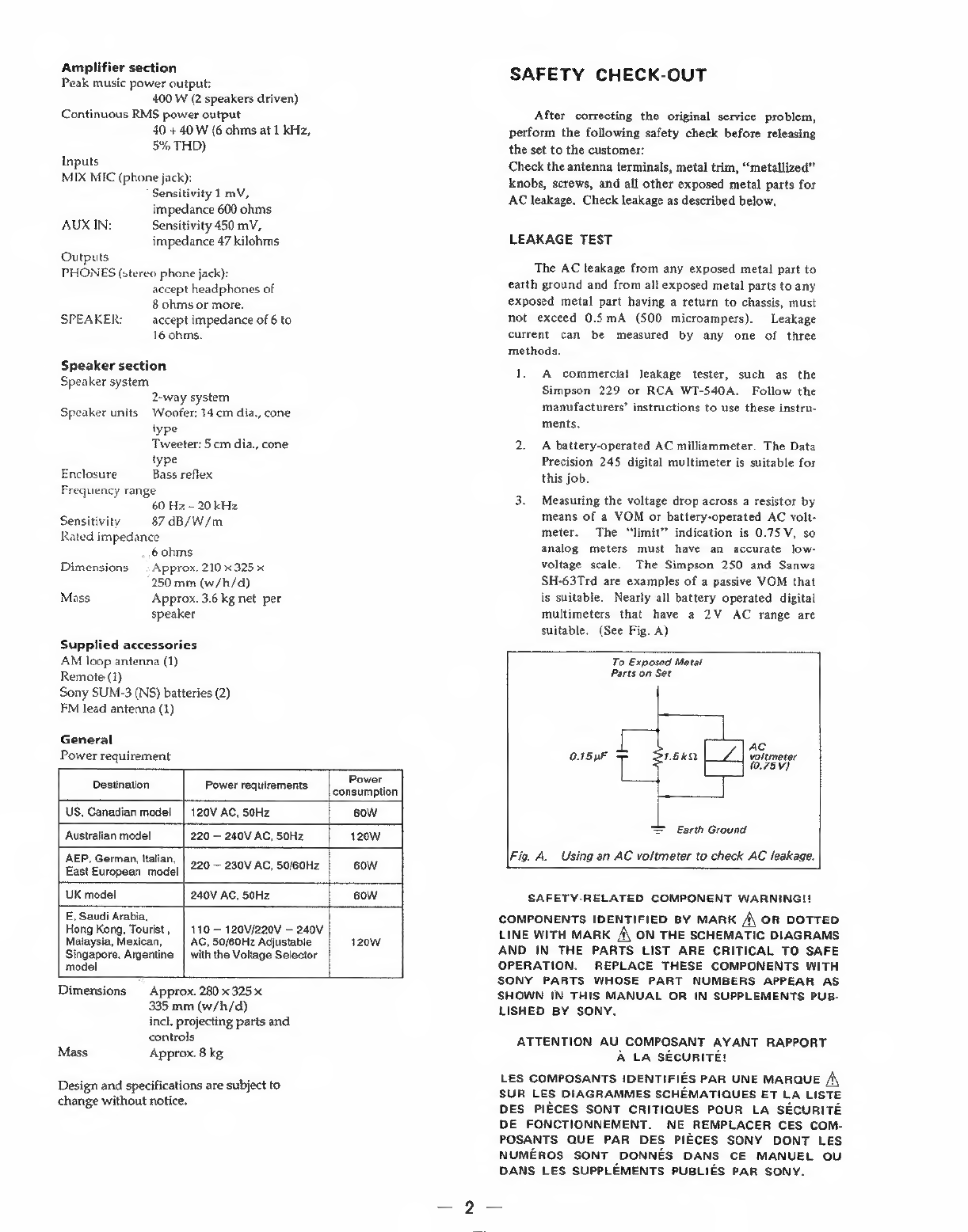
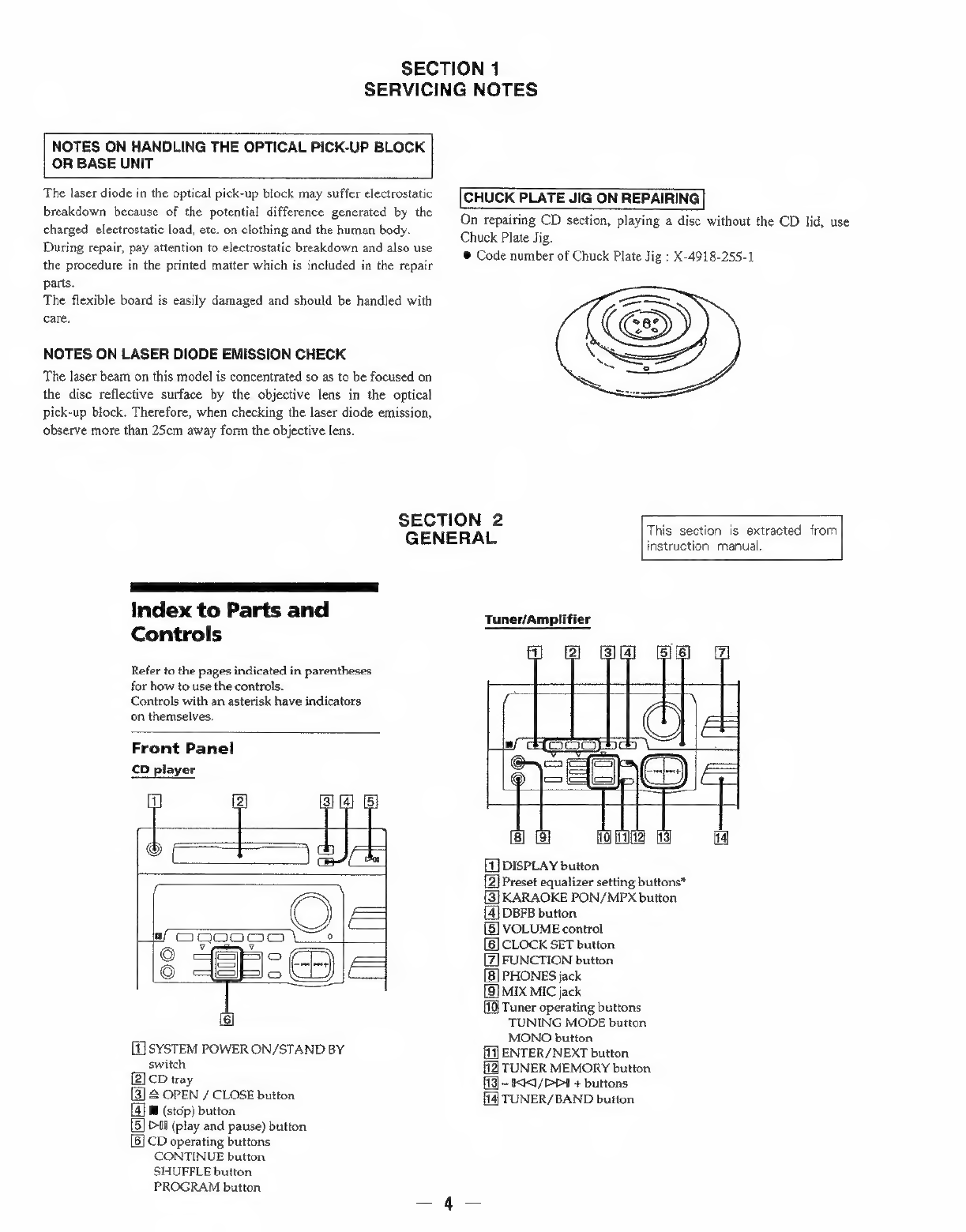
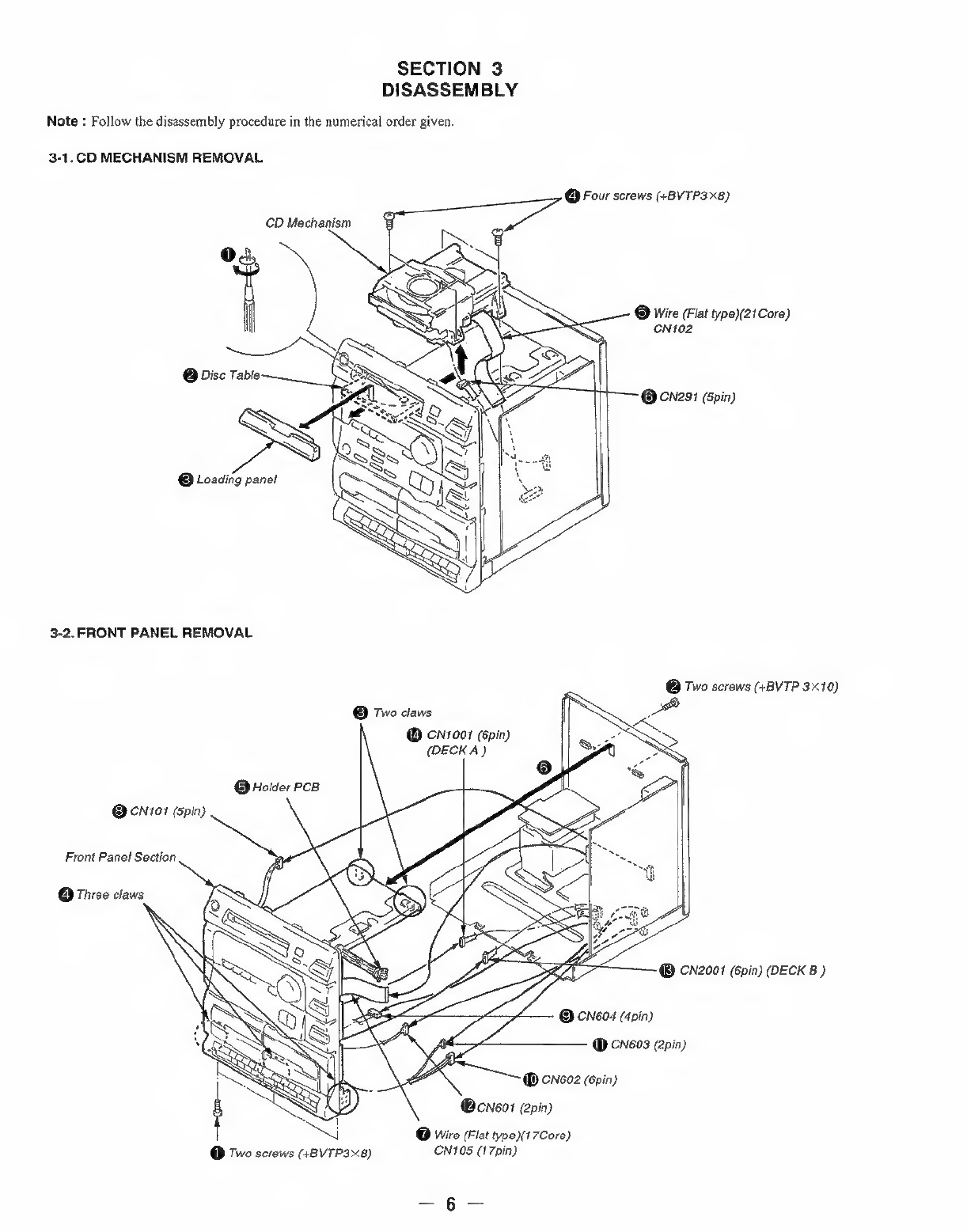
Sony FH-G50 User manual

FH-G50/MHC-501/$200
SERVICE
MANUAL
FH-G50
and
MHC-501/S200
are
composed
of
following
models.
As
for
the
service
manual,
it
is
issued
for
each
component
models,
then,
please
refer
to
it.
COMPONENT
MODEL
NAME
FOR
FH-G50
and
MHC-501/S200
US
Model
Canadian
Model
MHC-S200
AEP
Model
MHC-501
Component
2°"
|__FH-G50
MHC-501
MHC-S200
_E
Model
Tuner,
deck,
|
HCD-H501
Australian
Model
CD,
amplifier
Tourist
Mode!
Speaker
System
|
SS-H501
SS-H701
FH-G50
SPECIFICATIONS
PARTS
LIST
(Accessories
&
Packing
Materials)
Supplied
accessories
AM
loop
antenna
(1)
Remote
commander
(1)
Sony
SUM-3
(NS)
batteries
(2)
FM
lead
antenna
(1)
Design
and
specifications
are
subject
to
change
without
notice.
@
Abbreviation
CND
:
Canadian
MY:
Malaysia
IT
3
Italian
SP:
Singapore
G:
German
MX:
Mexican
EE
:EastEuropean
AR
:
Argentine
EA:
Saudi
Arabia
JE:
Tourist
AUS
:
Australian
HK
—:
Hong Kong
MICROFILM
9-960-149-11
Sony
Corporation
Consumer
A&V
Products
Company
Home
A&V
Products
Div.
NOTE:
@
Items
marked
“
*
"are
not
stocked
since
they
are
seldom
required
for
routine
service.
Some
delay
should
be
anticipated
when
ordering
these
items.
Part
No.
Description
1-473-039-11
COMMANDER,
STANDARD
(RM-S22)
1-501-374-11
ANTENNNA,
LOOP
1-501-594-11
ANTENNNA,
(FM)
(501:EXCEPT
G)
1-501-659-11
ANTENNNA,
(FM)
(G50,
$200)
1-769-306-11
CORD,
SPEAKER
(FOR
SS)
3-798-355-11
MANUAL,
INSTRUCTION
(ENGLISH)
(S200:US,
CND/G50:
AUS)
3-798-355-41
MANUAL,
INSTRUCTION
(FRENCH)
(S200:CND/G5O:E,
BA,
MY)
3-798-355-51
MANUAL,
INSTRUCTION
(ENGLISH/SPANISH/CHINESE)
(G50:E,
BA, SP,
MY,
MX, HK,
AR)
3-798-355-61
MANUAL,
INSTRUCTION
(ENGLISH/KOREAN/PORTUGUESE/
RUSSIAN)
(G50:
JE)
3-198-355-71
MANUAL,
INSTRUCTION
(ARABIC)
(G50:E,
BA)
3-198-356-41
MANUAL,
INSTRUCTION
acacia
rhage
(501:
AEP
3-798-356-51
MANUAL,
INSTRUCTION
(GERMAN)
(501:G)
3-798-356-61
MANUAL,
INSTRUCTION
(ITALIAN)
(501:ABP,
IT)
3-798-356-71
MANUAL,
INSTRUCTION
(ENGLISH/GERMAN)
(501:AEP,
EE)
3-798~-356-81
MANUAL,
INSTRUCTION
(RUSSIAN/POLISH)
(501:EE)
3-798-356-91
MANUAL,
INSTRUCTION
(DANISH,
FINNISH,
SWEDISH)
(501:
AEP)
4-941-762-01
COVER,
BATTERY
(FOR
RM-S22)
%
4-971-217-01
CUSHION
(FOR
SS)
*
4-972-969-01
CUSHION
(FRONT)
(FOR
HCD-501)
*
4-972-970-01
CUSHION
(REAR)
(FOR
HCD-501)
4-972-973-01
INDIVIDUAL
CARTON
(S200)
4-972-974-01
INDIVIDUAL
CARTON
(501:EXCEPT
EE)
4-972-975-01
INDIVIDUAL
CARTON
(5(
)
4-972-976-01
INDIVIDUAL
CARTON
(G50:AUS)
4-972-977-01
INDIVIDUAL
CARTON
(G50:AR,
B,
HK,
MX,
MY,
SP)
He
ee
¥
4-972-978-01
INDIVIDUAL
CARTON
(G50:EA,
JE)
MINI
Hi-Fi
COMPONENT
SYSTEM
SONY.
English
95B02102-1
Printed
in
Japan
4199.2
Published
by
Home
A&V
Products
Div.
Quality
Engineering
Dept.

SERVICE
MANUAL
@
HCD-H501
is
the
tuner,
deck,
CD
and
amplifier
section
in
FH-G50.
@
HCD-H501
is
the
tuner,
deck,
CD
and
amplifier
section
in
MHC-501
and
MHC-S200.
HCD-H501
US
Model
Canadian
Model
AEP.
Model
UK
Model
E
Model
Australian
Model
Tourist
Model
Photo
:
AEP
Model
Dolby
noise
reduction
manufactured
under
license
from
Model
Name
Using
Similar
Mechanism
HOD-H801
Dolby
Laboratories
Licensing
Corporation,
cD
.
“DOLBY”
and
the
double-D
symbol
DO
are
trademarks
of
|
section
CD
Mechanism
Type
CDM28-5BD19
Dolby
Laboratories
Licensing
Corporation.
Base
Unit
Name
BU-5BD19
Tape
deck
|Model
Name
Using
Similar
Mechanism
NEW
Section
Tape
Transport
Mechanism
Type
TCM180VW-H13
SPECIFICATIONS
CD
player
section
System
Compact
disc
digital
audio
system
Laser
Semiconductor
laser
Wavelength
780-790.
nm
Frequency
response
2
Hz~20
kHz
Tuner
section
FM
stereo,
FM/AM
superheterodyne
tuner
FM
tuner
section
Tuning
range
87.5
-108.0
MHz
(50
kHz
step
for
except
US,
Canadian,
East
European
model)
(100kHz
step
for
US,
Canadian
model)
FMI
:
65-
74MHz
(LOkHz
step)
FM2
:
87.5-
108MHz
(East
European
model)
Antenna
FM
lead
antenna
Antenna
terminals
75
ohm
unbalanced
Intermediate
frequency
10.7
MHz
AM
tuner
section
Tuning
range
US,
Canadian
model
:
AM
:
$30~
1,710kHz
(10kHz
step)
AM
:
$31
1,710kHz
(9kHz
step)
AEP,
UK,
East
European,
German
model
:
MW
:
531~
1,602kHz
(9kHz
step)
LW
:
153-279kHz
Italian
model
MW
:
522-
1,611kHz
(9kHz
step)
LW
:
153-279kHz
E,
Saudi
Arabia,
Argentine,
Hong
Kong,
Mexican,
Malaysia,
Singapore,
Australian,
Tourist
model
:
MW:
531
-
1,602
kHz
(9
kHz
step)
530
-
1,710
kHz
(10kHz
step)
SW:
5.95
-
17.9
kHz
(E,
Saudi
Arabia,
Hong
Kong,
Tourist,
Malaysia,
Singapore
model)
AM
loop
aerial
External
aerial
terminals
Intermediate
frequency
450
kHz
Tape
player
section
Recording
system
4-track
2-channel
stereo
Frequency
response
(DOLBY
NR
OFF)
60
~
13,000
Hz
(3
dB),
using
Sony
TYPE
I
cassette
60
-
14,000
Hz
(£3
dB),
using
Sony
TYPE
II
cassette
Wow
and
flutter
0.1%
WRMS
+0.3%
(DIN)
—
Continued
on
page
2
~
Antenna
COMPACT
DISC
DECK
RECEIVER
SONY.

Amplifier
section
Peak
music
power
output:
400
W
(2
speakers
driven)
Continuous
RMS
power
output
40
+
40
W
(6
ohms
at
1
kHz,
5%
THD)
Inputs
MIX MIC
(phone
jack):
Sensitivity
1
mV,
impedance
600
ohms
AUX
IN:
Sensitivity
450
mV,
impedance
47
kilohms
Outputs
PHONES
(stereo
phone
jack):
accept
headphones
of
8
ohms
or
more.
accept
impedance
of
6
to
16
ohms.
SPEAKER:
Speaker
section
Speaker
system
2-way
system
Speaker
units
Woofer:
14
cm
dia.,
cone
type
Tweeter:
5
cm
dia.
cone
type
Enclosure
Bass
reflex
Frequency
range
60
Hz,
-
20
kHz
Sensitivity
87
dB/W/m
Rated
impedance
6
ohms
Dimensions
_
Approx.
210
x
325
x
250
mm
(w/h/d)
Mass
Approx.
3.6
kg
net
per
speaker
Supplied
accessories
AM
loop
antenna
(1)
Remote
(1)
Sony
SUM-3
(NS)
batteries
(2)
FM
lead
antenna
(1)
General
Power
requirement
" 1
Power
Destination
Power
requirements
consumption
US,
Canadian
model_|
120V
AC,
S0Hz
60W
‘Australian
model
220
—
240V
AC,
S0Hz
120W
AEP,
German,
Italian,
5
East
European
model
220
—
230V
AC,
50/60Hz
60W
UK
model
240V
AC,
50Hz
6ow
E,
Saudi
Arabia,
Hong
Kong,
Tourist
,
110
—
120V/220V
—
240V
Malaysia,
Mexican,
|
AC,
50/60Hz
Adjustable
120W
Singapore,
Argentine
|
with
the
Voltage
Selector
model
Dimensions
—
Approx.
280
x
325
x
335
mm
(w/h/d)
incl.
projecting
parts
and
controls
Mass
Approx.
8
kg
Design
and
specifications
are
subject
to
change
without
notice.
SAFETY
CHECK-OUT
After
correcting
the
original
service
problem,
perform
the
following
safety
check
before
releasing
the
set
to
the
customer:
Check
the
antenna
terminals,
metal
trim,
“metallized”
knobs,
screws,
and
all
other
exposed
metal
parts
for
AC
leakage,
Check
leakage
as
described
below.
LEAKAGE
TEST
The
AC
leakage
from
any
exposed
metal
part
to
earth
ground
and
from
all
exposed
metal
parts
to
any
exposed
metal
part
having
a
return
to
chassis,
must
not
exceed
0.5mA
(S00
microampers).
Leakage
current
can
be
measured
by
any
one
of
three
methods.
1.
A
commercial
leakage
tester,
such
as
the
Simpson
229
or
RCA
WT-540A.
Follow
the
manufacturers’
instructions
to
use
these
instru-
ments.
2.
A
battery-operated
AC
milliammeter.
The
Data
Precision
245
digital
multimeter
is
suitable
for
this
job.
3.
Measuring
the
voltage
drop
across
a
resistor
by
means
of
a
VOM
or
battery-operated
AC
volt-
meter.
The
“limit”
indication
is
0.75V,
so
analog
meters
must
have
an
accurate
low-
voltage
scale.
The
Simpson
250
and
Sanwa
SH-63Trd
are
examples
of
a
passive
VOM
that
is
suitable.
Nearly
all
battery
operated
digital
multimeters
that
have
a
2V
AC
range
are
suitable.
(See
Fig.
A)
To
Exposed
Metal
Parts
on
Set
ac
0.15
uF
1.542
|_L£
|
voltmeter
(0.75
V)
=
Earth
Ground
Fig.
A.
Using
an
AC
voltmeter
to
check
AC
leakage.
SAFETY-RELATED
COMPONENT
WARNING!!
COMPONENTS
IDENTIFIED
BY
MARK
/\
OR
DOTTED
LINE
WITH
MARK
A\
ON
THE
SCHEMATIC
DIAGRAMS
AND
IN
THE
PARTS
LIST
ARE
CRITICAL
TO
SAFE
OPERATION.
REPLACE
THESE
COMPONENTS
WITH
SONY
PARTS
WHOSE
PART
NUMBERS
APPEAR
AS
SHOWN
IN
THIS
MANUAL
OR
IN
SUPPLEMENTS
PUB-
LISHED
BY
SONY,
ATTENTION
AU
COMPOSANT
AYANT
RAPPORT
A
LA
SECURITE!
LES
COMPOSANTS
IDENTIFIES
PAR UNE
MARQUE
/\,
SUR
LES
DIAGRAMMES
SCHEMATIQUES
ET
LA
LISTE
DES
PIECES
SONT
CRITIQUES
POUR
LA
SECURITE
DE
FONCTIONNEMENT.
NE
REMPLACER
CES
COM-
POSANTS
QUE
PAR DES
PIECES
SONY
DONT
LES
NUMEROS
SONT
DONNES
DANS
CE
MANUEL
OU
DANS
LES
SUPPLEMENTS
PUBLIES
PAR
SONY.

MODEL
IDENTIFICATION
TABLE
OF
CONTENTS
~
BACK
PANEL
—
Section
Title
Page
Specifications
(|
1
2.
GENERAL
Index
to
Parts
and
Controls-+-
SERVICING
NOTES
88
3.
DISASSEMBLY
3-1.
CD
Mechanism
Removal:
3-2.
Front
Panel
Removal:
3-3.
TC
Mechanism
Removal
-
4,
ADJUSTMENTS
4-1.
Mechanical
Adjustments
-
4-2,
Electrical
Adjustments~
5.
EXPLANATION
OF
IC
TERMINALS
---
4-972-055-0(]:
AEP
(AE1)
model
4-972-055-2(]:
Italian
model
4-972-055-3():
German
model
6.
DIAGRAMS
4-972-055-40:
UK
(UK2)
model
6-1.
Block
Diagram
—
CD
Section
—
4-972-055-5(]:
East
European
model
6-2,
Block
Diagram
—
Main
Section
—
eee
oe
ue
east
6-3.
Circuit
Board
Location
+
4-972-055-7():
Canadian
model
4-972-058-8(]:
AEP
(AE2)
model
6-4,
Printed
Wiring
Boards
—
Main
Section
~
4-972-055-90):
UK
(UK1)
model
6-5.
Schematic
Diagram
—
Main
Section
—
4-972-056-0(7:
E,
Argentine,
Tourist
model
6-6,
Schematic
Diagram
—
Panel
Section
—
4-972-056-1(]:
Saudi
Arabia
model
6-7.
Printed
Wiring
Boards
—
Panel
Section
4-972-056-2(]):
Australian
model
6-8.
Printed
Wiring
Boards
—
BD
Section
4-972-056-3(]:
Malaysia
model
4.972.056-40]:
Singapore
model
6-9.
Schematic
Diagram
—
BD
Section
—
4-972-056-5(]:
Hong
Kong
model
6-10.
IC
Block
Diagrams
4-972-056-6[_]:
Mexican
model
7.
EXPLODED
VIEWS
7-1.
Chassis
Section--
7-2,
Front
Panel
Section:
7-3.
Mechanism
Deck
Section-
7-4,
Mechanism
Deck
Section-:
7-5.
Mechanism
Deck
Section-
7-6.
CD
Mechanism
Section:
This
appliance
is
classified
as
a
7-7,
Base
Unit
Section:
CLASS
1
LASER
PRODUCT
CLASS
1
LASER
product.
The
CLASS
1
LASER
LUOKAN
1
LASERLAITE
i
KLASS
1
LASERAPPARAT
PRODUCT
MARKING
is
located
on
the
rear
exterior.
Laser
component
in
this
product
is
capable
of
emitting
radiation
exceeding
the
limit
for
Class
1.
8.
ELECTRICAL
PARTS
LIST
-
This
caution
CAUTION.
Russe
usemnananon
wen
Oren
label
is
located
T"USYNUG
LASERSTARUNG
VED
ABNING
NAA
i
ADVARSEL
|
SiocenhcoSaFanvOERE
ER
LOE
AF
FUNKTION
inside
the
unit.
UnOGA
ude
AETTELSE
FO}
VARO!
7
AVATTAESSA
JA
SUQUALUKITUS
OHITETTAESSA
WARNING;
USERSTRAUNG
Nan
DchNa
DEL
AR
OPPNAD
OCH
SPARREN
AA
URXOPPLAD,
|
USYNUG
LASERSTRALING
NAA
OEKSEL
APnt
ADVARSEL
i
Uhnc
EXSPONEFING
POR
STHALEN
CAUTION
Use
of
controls
or
adjustments
or
performance
of
procedures
other
than
those
specified
herein
may
result
in
hazardous
radiation
exposure.

SECTION
1
SERVICING
NOTES
NOTES
ON
HANDLING
THE
OPTICAL
PICK-UP
BLOCK
OR
BASE
UNIT
The
laser
diode
in
the
optical
pick-up
block
may
suffer
electrostatic
breakdown
because
of
the
potential
difference
generated
by
the
charged
electrostatic
load,
etc.
on
clothing
and
the
human
body.
During
repair,
pay
attention
to
electrostatic
breakdown
and
also
use
the
procedure
in
the
printed
matter
which
is
included
in
the
repair
parts.
The
flexible
board
is
easily
damaged
and
should
be
handled
with
care.
NOTES
ON
LASER
DIODE
EMISSION
CHECK
The
laser
beam
on
this
model
is
concentrated
so
as
to
be
focused
on
the
disc
reflective
surface
by
the
objective
lens
in
the
optical
pick-up
block.
Therefore,
when
checking
the
laser
diode
emission,
observe
more
than
25cm
away
form
the
objective
lens.
CHUCK
PLATE
JIG
ON
REPAIRING
On
repairing
CD
section,
playing
a
disc
without
the
CD
lid,
use
Chuck
Plate
Jig.
©
Code
number
of
Chuck
Plate
Jig
:
X-4918-255-1
——
ort
28S
SECTION
2
-
Thi
ti
tracted
from
GENeEnOS
patunlon
marae
gs
ET
SRS
Index
to
Parts
and
ee
Controls
Tuner/Ampiifier
Refer
to
the
pages
indicated
in
parentheses
for
how
to
use
the
controls.
Controls
with
an
asterisk
have
indicators
on
themselves.
Front
Panel
DISPLAY
button
Preset
equalizer
setting
buttons*
KARAOKE
PON/MPX
button
1]
SYSTEM
POWER
ON/STAND
BY
switch
(2)cD
tray
&
OPEN
/
CLOSE
button
M
(stop)
button
5]
Dil
(play
and
pause)
button
[6]
CD
operating
buttons
CONTINUE
button
SHUFFLE
button
PROGRAM
button
DBFB
button
VOLUME
control
CLOCK
SET
button
FUNCTION
button
PHONES
jack
MIX MIC
jack
Tuner
operating
buttons
TUNING
MODE
button
MONO
button
fi]
ENTER/NEXT
button
[f
TUNER
MEMORY
button
[13]
-144/>>4
+
buttons
14
TUNER/BAND
button
BeBseeseNe

Function
indication
CD
play
mode
indications
Music
calendar
DBEB
indication
AUTO/TUNING/PRESET/STEP
indications
Frequency
/time
indication
Tuner/Karaoke
indications
VOLUME
indication
Tape
player
Cvs
|coiosres
isis
Remote
(RM-S22)
1
2
3
7]
DOLBY
NR
button*
3
[2]
Tape
compartments
[3]
Tape
operating
buttons
4
5
=
=
&
(play)
>>
(fast
rightward)
5
“4
(fast
leftward)
WA
(stop
play/eject)
@
(recording)(for
deck
B
only)
ik
IN
(pause)
(12)
Rear
panel
AEP,
G,
IT,
BE,
EXCEPT
AEP,
G,
IT,
UK
model
EE,
UK
model
6
7]
SLEEP
button
[2]
FUNCTION
button
3]
MD
operating
buttons
_
=
>
(play)
button
E,
EA,
SP,
AR,
H
(pause)
button
—
JE,
HK
model
(stop
play)
button
5
a
CD
operating
buttons
Leese
—
>
(play)
button
1
(pause)
button
3]
(stop
play)
button
H44
/P
>I
(AMS)
buttons
Tove
Cr
ere
mais
(fast
forward
/fast
reverse)
uttons
AEP,
G,
IT,
EE,
UK
model
REPEAT
bullion
T]
FM
75
Q
terminal
:
EDIT
button
EXCEPT
AEP,
G,
IT,EE,
UK
model
CHECK
button
(2)
+
earth
terminals
CLEAR
button
[3}
AM
terminal
5]
Tuner
operating
buttons
[4]
AUX
IN
jacks
BAND
button
[5]
SPEAKER
connectors
PRESET
(+/-)
buttons
[6]
-b
ground
terminal
6]
SYSTEM
POWER
button
7)
VOLTAGE
SELECTOR
:E,
EA,
SP,
AR,
JE,
HK
model
7)
VOL(+/-)
buttons
8]
Power
cord
Display
window
+
Abbreviation
G
:German
a
2)
[3]
4
IT:
Italian
EE
:
East
European
port,
|_|
SIE
EA
:
Saudi
Arabia
St
(PEI
AR
:
Argentine
aa
oat
HK
:
Hong Kong
farsa
||
cok
JE
:
Tourist
SP
:
Singapore
5 6 Z

SECTION
3
DISASSEMBLY
Note
:
Follow
the
disassembly
procedure
in
the
numerical
order
given.
3-1.
CD
MECHANISM
REMOVAL
@
Four
screws
(+BVTP3X8)
CD
Mechanism
Wire
(Flat
type)(21Core)
CN102
@cnz291
(Spin)
©
Loadirig
panel
3-2.
FRONT
PANEL
REMOVAL
@
Two
screws
(+BVTP
3X10)
©
Two
claws
ie
@CN101
(Spin)
Front
Panel
Section
@
Three
claws
@®
€N2001
(6pin)
(DECK
B
)
©
CN604
(4pin)
®
cn603
(2pin)
@
CN602
(6pin)
@ecneot
(2pin)
—~Gn
I
Pei
@
Wire
(Flat
type)(17Core)
@
Two
screws
(+BVTP3X8)
CN105
(17pin)
6s

3-3.
TC
MECHANISM
REMOVAL
@
Six
screws
(+BVTP2.6%6)
@
Eject
button
TC
Mechanism
@
Lid
(8)
assy,
cassette

SECTION
4
ADJUSTMENTS
4-1,
MECHANICAL
ADJUSTMENTS
PRECAUTION
1.
Clean
the
following
parts
with
a
denatured-alcohol-
moistened
swab
:
record/playback
head
pinch
roller
erase
head
rubber
belts
capstan
idlers
2.
Demagnetize
the
record/playback
head
with
a
head
demagnetizer.
3,
Do
not
use
a
magnetized
screwdriver
for the
adjustments.
4,
After
the
adjustments,
apply
suitable
locking
compound
to
the
parts
adjusted.
5.
The
adjustments
should
be
performed
with
the
rated
4-2,
ELECTRICAL
ADJUSTMENTS
DECK
SECTION
1,
The
adjustment
should
be
performed
in
the
publication.
(Be
sure
to
make
playback
adjustment
at
first.)
2.
The
adjustment
and
measurement
should
be
performed
for
both
L-CH
and
R-CH.
©
Switch
position
DOLBY
NR
switch
:
OFF
FUNCTION
button
:
CD
3.
Deck
section
electrical
adjustments
are
made
in
test
mode
by
pressing
TUNER/BAND,
DISPLAY,
and
POPS
at
the
same
time.
4.
Input point
and
output
level
measurement
point.
power
supply
voltage
unless
otherwise
noted.
Output
level
measurement
Input point
point
@
Torque
Measurement
36.7mV
( ~
25.648)
AF
OSC
-
a
are
Mode
|
Torque
Meter
Meter
Reading
lene
ste
30
to
70gcm
measurement
Forward
ora
(0.42
=
0.97
ozsinch)
point
wee
peed
ooclt.
R-CH
Forward
1.5
to
5.5geom
Back
Tension]
CQ-102C
(0.021
—
0.076
ozsinch)
aes
onaoe
9
1
more
than
63gscm
FF,
REW
cO-2018
‘oes
earehy
MAIN
BOARD
1
3
CNéoT
©
Test
Tape
Tape
Contents
Use
P-4-A100
10kHz,
~
10dB
Head
Azimuth
Adjustment
P-4-L300
315Hz,
0dB
Level
Adjustment
WS-48B
3kHz,
Od
Tape
Speed
Adjustment
0
dB=0.775V
DECK
A
Procedure
:
1.
Forward
Playback
mode
Reverse
Playback
mode
test
tape
P-d-A100
(fokHz,
~
1008)
RS
Record/Playback
Head
Azimuth
Adjustment
DECD
B
‘Output
level
measurement
point

2.
Tum
the
adjustment
screw
for
the
maximum
output
levels.If
these
levels
do
not
match,turn
the
adjustment
screw
until
both
of
output
levels
match
together
within
1dB.
LcH
peak
output
level
RCH
peak
Screw
position
—
screw
angie
peak
peak
3.
Playback
Mode
test
tape
Ba.Atoo
(10K,
~
10<8)
L-CH
Oscilloscope
SS
L
nd
R
ics
Pee
>
Te)
F
RecH
Cutout
fevel
measurement
point
(see
page
8)
Scjean
pater
in
phase
90°
135° 1805
good
wrong
4.
Change
the
review
playback
mode
and
repeat
the
steps
1
to
3.
5,
After
the
adjustment,
lock
the
adjustment
screw
with
suitable
locking
compound,
Adjustment
Location
:
—
record/playback
head
(Deck
A
and
Deck
B)
—
adjustment
screws
DECK
Aj
|DECK
B
Tape
Speed
Adjustment
Procedure
:
©
Perform
high
speed
adjustment
before
normal
speed
adjust-
ment.
Mode
:
Playback
fost
tape
(Rie,
G8)
jek
1.
Set
to
FWD
playback
mode.
2.
Adjust
RV670
so
that
the
frequency
counter
reading
becomes
3,000
+
1SHz.
frequency
counter
‘Output
level
measurement
point
(see
page
8)
Frequency
difference
between
the
begining
and
the
end
of
the
tape
should
be
within
+
3%.
Adjustment
Location
:
MAIN
board.
(see
page
10)
DECK
B
DECKA
Playback
Level
Adjustment
Procedure
:
Mode
:
Playback
test
tape
P-4-1300
(315Hz,
008)
vive
set
“Ss
‘Output
level
measurement
point
(See
page
8)
Deck
A
is
RV601(L-CH)
and
RV651(R-CH),
deck
B
is
RV602
(L-CH)
and
RV652
(R-CH)
so
that
adjustment
within
adjustment
level
as
follows.
Adjustment
Level
:
LINE
OUT
level
:
—
7.5
+
0.5dB
(0.31
to
0.35V)
Level
Difference
between
Channels
:
within
0.5dB
Confirm
the
DOLBY
OUT
level
does
not
change
in
playback
mode
while
changing
the
mode
from
playback
to
stop
several
times.
Adjustment
Location
:
MAIN
board.
(see
page
10)

Record
Bias
Adjustment
|DECK
B Record
Level
Adjustment
|DECK
B
Procedure
:
FUNCTION
button
:
CD
1.
Record
mode
Procedure
:
1.
Record
mode
AF
OSC
1316:
36.7mV(
~
26.508)
pant
ae
AF
OSC
anid
315Hz,
36.7mV{
~
26.58)
Blanklepe
attenvator
8-123,
o
€)
ark
TP
ooo
Z|
_atonuator
oo
on
°
‘oo
°
———!
I|ooo
ld
Ce
be
input
point
(see
page
8)
input
point
(see
page
8)
2.
Playback
mode
2.
Playbacd
mode
recorded
porien,
Med
recorded
zi
orton
viv
2,
ae
ae
ss
‘Qulput
leve!
measurement
point
aS
(see
page
8)
utput
lave!
measurement
point
" + *
(see
page
8)
3.
Confirm
playback
the
signal
recorded
in
step
1
become
adjustment
level
as
follows.
3.
Confirm
playback
the
signal
recorded
in
step
become
4, If
these
levels
do
not
adjustment
level,
adjustment
the
RV620
adjustment
level
as
follows.
(L-CH)
and
RV630
(R-CH)
to
repeat
step
1
and
4. 4,
If
these
levels
do
not
adjustment
level,
adjustment
the
RV401(L-CH)
and
RV451
(R-CH)
to
repeat
step
I
and
4,
Adjustment
level
:
Playback
output
of
315Hz
to
playback
output
|
Adjustment
Level
:
of
10kHz
:
—
0.5dB
to
0.5dB.
DOLBY
OUT
level
:
—
22.5dB
+
0.5dB
(54.9
to
61.6mV)
(=
1.3
to
1.3mvV)
Adjustment
Location
:
MAIN
board
Adjustment
Location
:
MAIN
board.
Adjustment
Location
:
[MAIN
BOARD}
—
Component
side
—
|
TBI0t
TMi
Fer
‘RV620
:
Record
Level
Adjustment
(L-CH)
RV630
:
Record
Bias
Adjustment
(A-CH)
RV60!
:
Playback
Level
Adjustment
(Deck
A
L-CH)
AV651
:
Playback
Level
Adjustment
(Deck
A
R-CH)
RVASI
:
Record
Level
Adjustment
(R-CH)
AVA01
:
Record
Level
Adjustment
(L-CH)
'RV602
:
Playback
Level
(Deck
B
L-CH)
AV670
:
Tape
Speed
Adjustment
RV652
:
Playback
Level
(Deck
B
R-CH)
—~
10
—

TUNER
SECTION
Note.
1
:
The
adjustment
should
be
performed
in
the
publication.
(AM
FM->
SW)
Note.
2:
As
a
front-end
(FEL)
is
difficult
to
repair
if
faulty,
replace
it
with
new
one.
AM
Section
Adjustment
Setting
:
60cm
——»|
loop
antenna
B
loop
antenna
A
C
s
a
ES
pel
AM
rf
signal
‘generator
30%
amplitude
modulation
by
400H2
signal
FM
Section
Adjustment
Setting
:
FM
rf
stereo
signal
generator
FM
ANTENNA
terminal
(TM1)
75
2
coaxial
Carrer
frequency
:
98MHz
‘modulation
:
1ktlz,
75kHz
deviation
AM
Tuned
Indication
Lighting
Level
Adjustment
Band
:
MW
Procedure
:
1.
Set
loop
antenna
A
so
that
the
loop
antenna
B
input
level
becomes
3.2mV
(70dB
«
)
2.
Tune
the
set
to
999kHz.
3.
Adjust
RV41
so
that
the
[TUNED]
light
up.
4.
Confirm
that
the
|TUNED]
light
off
with
AM
RF
SG
output
level
set
at
OdBy
.
S.
Confirm
the
FM
tuned
indication
lighting
level
and
adjust
if
necessary.
Adjustment
Location
:
Main
board
Adjustment
Location
:
[MAIN
BOARD)
—
Component
side
—
TBIOt
TM
FEL
FM
Tuned
Indication
Lighting
Level
Adjustment
Band
:
FM
Procedure
:
1.
Supply
a
11.2”V
(21dBjz)
98MHz
signal
to
the
ANTENNA
terminal.
2.
Tune
the
set
to
98MHz.
3,
Adjust
RV42
so
that
the
|
TUNED
]light
up.
4.
Confirm
that
the
[TUNED]
light
off
with
FM
RF
signal
generator
output
level
set
at
16dBy
.
Adjustment
Location
:
Main
board
SW
OSC
Voltage
Adjustment
Band
:
SW
(E3,
Saudi
Arabia,
Hong
Kong,
Malaysia,
Singapore
model)
Procedure
:
1.
Connecct
the
VOM
to
JW376
(OSC)
2.
Tune
the
set
to
S.9SMHz.
3.
Adjust
T2
for
1.0
to
1.1V
reading
on
the
VOM.
4,
Tune
the
set
to
17.90MHz.
5.
Adjust
CV2
for
8.4
to
8.6V
reading
on
the
VOM.
SW
Tracking
Adjustment
Band
:
SW
Procedure
:
1.
Connect
the
VOM
to
speaker
terminal.
(TB101)
2.
Adjust
for
a
maximum
reading
on
VOM.
‘Signal
generator
and
set
frequency
7.0
MHZ
Th
Adjustment
part
17.0
MHZ
cvL
Adjustment
Location
:
Main
board
a
|
~~
AV42
:
FM
Tuned
indleation
Lighting
Level
Adjustment

CD
SECTION
Note
:
1.
CD
Block
basically
constructed
to
operate
without
adjust-
ment.
Therefore,
check
each
item
in
order
given.
2.
Use
YEDS-18
disc
(3-702-101-01)
unless
otherwise
indi-
cated.
3.
Use
the
oscilloscope
with
more
than
10M
Q
impedance.
4,
Clean
an
object
lens
by
an
applicator
with
neutral
detergent
when
the
signal
level
is
low
than
specified
value
with
the
following
checks.
Focus
Bias
Adjustment
This
adjustment
is
to
be
done
when
the
optical
block
is
replaced.
Adjustment
procedure
:
oscilloscope
(OC
range)
BD
board
O
TRA)
oF
TP
(VC)
-
.
Connect
oscilloscope
to
test
point
TP
(VC)
and
TP
(RF)
on
main
board.
..
Turned
power
switch
ON.
(Stop
mode)
.
Put
disc
(YEDS-18)
in
and
press
the
D>
button.
.
Press
the
DISPLAY/ENTER
button.
(Tracking
servo
ON)
.
Adjust
RV101
so
that
the
oscilloscope
waveform
is
as
shown
in
the
figure
below
(eye
pattern).
A
good
eye
pattern
means
that
the
diamond
shape
(<>)
in
the
center
of
the
waveform
can
be
clearly
distinguished.
.
Release
test
mode
after
adjustment
is
completed.
WRWN
a
©
RF
signal
reference
waveform
(eye
pattern)
SOV
VER
|
ee
WY
VoLT/DIV:
0.2V
TIME/DIV
:
500ne
iM
NY
#04
WANN
L
When
observing
the
eye
pattern,
set
the
oscilloscope
for
AC
range
and
raise
vertical
sensitivity.
S-Curve
Check
oscilloscope
BD
board
ame
O
TR
(FEO)
o—e——+
TP(VC)
o=—t————-0
-
Procedure
:
1.
Connect
oscilloscope
to
test
point
TP
(FEO)
and
BD
board.
2.
Connect
between
test
point
TP
(FOK)
and
GND
by
lead
wire.
3.
Turned
Power
switch
on.
4,
Put
disc
(YEDS-18)
in
and
turned
Power
switch
on
again
and
actuate
the
focus
search.
(actuate
the
focus
search
when
disc
table
is
moving
in
and
out.)
5.
Check
the
oscilloscope
waveform
(S-curve)
is
symmetrical
between
A
and
B.
And
confirm
peak"to
peak
level
within
3.8
1.1Vp-p.
S-curve
waveform
symmetry
within
3.8
+
1.1Vp-p
6.
After
check,
remove
the
lead
wire
connected
in
step
2.
Note
:
@
Try
to
measure
several
times
to
make
sure
that
the
ratio
of
A:BorB:
A
is
more than
10:
7.
©
Take
sweep
time
as
long
as
possible
and
light
up
the
brightness
to
obtain
best
waveform.
RF
Level
Check
oscilloscope
BD
board
O
TRA)
o—t——-0-
+
TP
(VC)
o=———0
-
Procedure
:
1.
Connect
oscilloscope
to
test
point
TP
(RF)
on
BD
board.
2.
Tumed
Power
switch
on.
3.
Put
dise
(YEDS-18)
in
and
playback.
4.
Confirm
that
oscilloscope
waveform
is
clear
and
check
RF
signal
level
is
correct
or
not.
Note
:
Clear
RF
signal
waveform
means
that
the
shape
“
©
clearly
distinguished
at
the
center
of
the
waveform.
can
be
VOLT
/
DIV:
200mV
TIME
/
DIV
:
5000S
RF
signal
waveform
‘"
Nt,
\)
Kyi
RR
NANI
SA
level:
1.3
+
0.3Vp-p
E-F
Balance
Check
oscllioscope
(OC
range)
BD
board
O
TP
(TEO)
=F
TP
(VO)
Procedure
:
1.
Ground
main
board
IC1O1
pin
@
with
the
lead
wire.
2.
Connect
oscilloscope
to
test
point
TP
(TEO)
on
BD
board.
3.
Turned
Power
switch
on.
4,
Put
disc
(VEDS-18)
in
and
playback.
5.
Confirm
that
the
osilloscope
waveform
is
symmetrical
on
the
top
and
bottom
in
relation
to
OV,
and
check
this
level.
—12—

Traverse
waveform
4
Vea
My
a
symmetry
level:
300
+
100mVp-p
6.
Remove
the
lead
wire
connected
in
step
1.
Focus/Tracking
Gain
This
gain
has
a
margin,
so
even
if
it
is
slightly
off.
There
is
no
problem.
Therefore,
do
not
perform,
this
adjustment.
Please
note
that
it
should
be
fixed
to
mechanical
center
position
when
you
moved
and
do
not
know
original
position.
Adjustment
Location
:
{BD
BOARD]
—
Component
side
—
3

1C101
TMP87CP64F-6254
SECTION
5
EXPLANATION
OF
IC
TERMINALS
Pin No. Pin
name
vo
Description
1
Vss
~
[GND
2
X
OUT
oO
|
?
Main
system
clock.
(8MHz)
3
XIN
i
4
RESET
1__|
Reset
signal
input
terminal.
5
X
OUT
oO
|
Sub
system
clock.
(32.768kHz)
6
XIN
I
7
GND
-
|
GND
8
AC
OUT
I
|
MICON
AC
DET.
9
COUNT
SW
=
|
Not
used.
(“H”
LEVEL)
10
INIT
SW
=
|
Not
used.
(“H”
LEVEL)
1
DISC
SENS
=
|
Not
used.
(“H”
LEVEL)
12
MID
SENS
=|
Not
used.
(“H”
LEVEL)
13
CD
XRST
O
|
CDReset
output.
“L”
:
RESET
14
POWER
O
|
Poweron
output.
“L”:
ON
15
TA
MUTE
QO
|
AMP
Mute
output.
“L”
:
MUTE
16
MPX
O
|
MPX
Control
output.
7
KEYCON
LATCH
—__|
Not
used.
(OPEN)
18
VOL
LATCH
©
|
Latch
output
to
volume
control.
(TC9210P)
19
K.PONA
=
|
Not
used.
(OPEN)
20
K.
PON
B
~_
|
Not
used.
(OPEN)
]
FUNCTION
|
FUNC
A
|
FUNC
B
21
FUNC
A
fo)
st
=
a
+
Function
Select.
cD
ig
H
2
FUNC
B
o
||
ie
H
:
AUX
H H
23
FUNC
C
—__|
Not
used.
(OPEN)
24
GEQ.
LATCH
O
|
Latch
output
to
gray
control.
(M62423FP)
25
RDS.
INT
1]
RDS
DATA
START
Signal
input.
26
‘SCOR
(DSP)
1__|
Sub-code
syne
SO+SI
detection
input
from
DSP.
(CXD2507AQ)
27
SENS
I__|
SENS
input
from DSP.
(CXD2507AQ)
28
CD
POWER
O
|
Power
on
output.
“H”
ON
29
CDG
LATCH
|
Not
used.
(OPEN)
:
30
DBFB
O
|
DBFB
Select
output.
“H”:
DBFB
LOW
“L”
:
DBFB
HIGH
31
ST
MUTE
0]
TUNER
MUTE
Output
32
STCE
O
|
Chip
enable
output
to
tuner
PLL
IC
(LC72130)
33
STEREO
1__[
FM/AM
Stereo
identification.
“L”
:
STEREO
34
TUNED
1
|
FM/AM
Tuning
identification."
“L”
:
TUNING
35
SQ-RDS-CLK
O
_|
Sub-code
Q
data
scanning
clock
output
to
DSP
(CXD2507AQ),
RDS
clock
output.
36
SQ-RDS-DI
1_[
Sub-code
Q
data
input
from
DSP
(CXD2507AQ),
RDS
data
input.
37
RDS-RESET
©
|
RDS
Reset
signal
output.
38
CLK
O_|
System
clock
output,
39
D.IN
1
|
Serial
data
input
from
tuner.
40
D.
OUT
O_|
Serial
data
(COMN)
output.
41
TABLE
SENS
—__
|
Not
used.
(OPEN)
42
REQ
GM
1__|
Data
transmission
request
input
from
system
control.
aan)

Pin No.
Pin
name
vo
Description
43
REQ
MG
fe)
Data
transmission
request
output
to
system
control.
44
CLK
MG
fe)
Clock
output
for
communications
with
system
control.
45
D.GM
I
Serial
data
input
form
system
control.
46
D.
MG
O
|
Serial
data
output
to
system
control.
47
RDY
1/0
|
System
control
Ready
signal
input/output.
“L”
:
READY
48
VAREF
—
|
Power
suppiy.
(+5V)
49
VASS
=
GND
50
Vss
e
GND
SI
Vp
—
|
Power
supply
(+5V)
52
URGENT.
SIG
I
Not
used.
(+5V)
53
URGENT.
STBY
i
Not
used.
(OPEN)
54
BUG
Y/N
-
|
Not
used.
(GND
Connected)
55
ADJUSTOR
—
|
Not
used.
(“H”
LEVEL)
56
ADJUST2
=
Not
used.
(“H”
LEVEL)
S?
MAGIC
SPEED
zd
Not
used.
(“H”
LEVEL)
58
SPEC
mm
Not
used.
(“H”
LEVEL)
59
DIST
mee
Not
used.
(“H”
LEVEL)
60
SPEED
*
Not
used.
(“H”
LEVEL)
61
BREAK
—__|
Not
used.
(“H”
LEVEL)
62
B-PLAY
1__|
Deck-B
PLAY
Switch
input.
“H”
:
PLAY
63
B-SHUT
—
|
Not
used.
(+5V)
64
B-HALF
—
|
Not
used.
(+5V)
65
A-SHUT
=
|
Not
used.
(+5V)
66
A-PLAY
I
Deck-A
PLAY
Switch
input.
“H”
:
PLAY
67
A-HALF
I
Deck-A
HALF
SW
input.
68
CAPM
H/L.
~
|
Not
used.
(OPEN)
69
CAPM
ON/OFF
Not
used.
(OPEN)
70
TRIG
H/L
i
nm
BTRG
—
|
}Not
used.
(OPEN)
72
ATRG
a
73
RELAY
oO
Control
output
to
REC/PB
select
switch.
(IC602)
74
AIB
Oo
Dolby
IC
PB
input
Deck
A/B
select
output.
“L”:
A,
“H":B
75.
NORM/HIGH
ad
Not
used.
(OPEN)
76
BIAS
ON/OFF
oO
BIAS
Oscillation
ON/OFF
control.
“H’”
:
ON
77
RM
ON/OFF
oO
REC
Mute
output.
“L”
:MUTE
78
REC/PB
oO
DOLBY
IC
REC/PLAY
Select
output.
“H”
:
REC
79
NR
oO
DOLBY
ON/OFF
Control
output.
“H”
:
ON
80
LM
oO
LINE
Mute
output.
“L”
:
MUTE,
81
PASS
©
_|
PASS
Amplifier
switch
output
to
DOLBY
IC.
(IC401)
82
CDG.
MUTE
—__|
Not
used.
(OPEN)
83
UP
MOTOR
ran
Not
used.
(OPEN)
84
DOWN
MOTOR
i
Not
used.
(OPEN)
85
TABLE
R
Not
used.
(OPEN)
86
TABLE
L
-
Not
used.
(OPEN)
87
LOAD
OUT
O
|
Loading
motor
(M903)
Load
out
output.
88
LOAD
IN
O
|
Loading
motor
(M903)
Load
in
output.
89
DF-LATCH
ie)
Latch
output
to
digital
filter.
(PCM1701U)
—45=

Pin No. Pin
name
vo
Description
90
XLT
ie}
Serial
data
latch
output
to
DSP.
(CDX2507AQ)
91
FOCUS
SW
O.
|
High-region
gain
down
output
to
focus
servo.
(CXA1782BQ)
92
HIGH
DUBB
i
Not
used.
(“H”
LEVEL)
93
TEST
1
=~
Not
used.
(“H”
LEVEL)
94
OUT
SW
1
|
CD
Tray
output
detection
input.
95
IN
SW
I
CD
Tray
input
detection
terminal.
96
UP
SW
—
|
Not
used.
(GND)
7
PANEL
SW
Ga
Not
used.
(GND)
98
CLOSE
SW
Not
used.
(GND)
99
OPEN
SW
aca
Not
used.
(GND)
100
Vp
—
|
Power
supply.
(+5V)

1C501
CXP82612-006Q
Pin
No.
Pin
name
vo
Description
z
ENC1A
I
Volume
encoder
input
terminal.
2
SIRCS*
1
|
Remote
commander
signal
input.
-
REQ.
MG
I
Data
transmission
request
input
from
master
control.
4
REQ.
GM
Oo
Data
transmission
request
output
to
master
control
5
LED1
—
|
Not
used.
(OPEN)
6
LED2
—
|
Not
used.
(OPEN)
7
LED3
—__|
Not
used.
(OPEN)
8
LED4
Not
used.
(OPEN)
9
LEDS
—
|
Not
used.
(OPEN)
10
RDY
VO
|
Master
control
Ready
signal
input/output.
“L”
:
Ready
lL
SCK.
IN
I
Clock
output
for
communications
with
master
control.
12
SD.
IN
I
Serial
data
input
from
master
control.
13
SD.
OUT
oO
Serial
data
output
to
master
control.
14
LED6
oO
REC,
PAUSE
LED
Output.
1S:
LED7
oO
ROCK,
USER
FILE
LED
Output.
16
LED8&
oO
JAZZ,
POPS
LED
Output.
17
LED9
oO
CLASSIC,
DANCE
LED
Output.
18
LEDIO
oO
TUNER
LED
Output.
19
LED11
oO
CD,
TIMER
LED
Output.
20
LEDI2
—_
|
Not
used.
(OPEN)
21
LEDI3
Not
used.
(OPEN)
22
KEY]
i
23
KEY2
I
Key
input.
(A/D
Converter)
24
KEY3
I
25
KEY4
—_
|
Not
used.
(+5V)
26
BPF1
I
27
BPF2
it
Not
used.
(+5V)
28
BPF3
I
29
BPF4
I
30
RST
I
|
Reset
signal
input
terminal.
31
XIN
T
:
7)
XOUT
ro)
System
clock.
(4MHz)
33
Vss
cal
GND
34
ANI
o
|)
35
AN2
le}
36
AN3
fe)
37
AN4
oO
LCD
Drive.
38
ANS
ie}
39
AN6
ie}
40
AN7
fe)
=r

Pin
No.
Pin
name
vo
Description
41
AN8,
oO
42
ANS
oO
43
ANIO
ie}
44
ANIL
oO
45
ANI2
oO
46
ANI3
oO
AT
ANI4
oO
48
ANIS
ie}
49
ANI6
ie}
50
ANI7
oO
SL
ANI8
oO
52
ANI9
oO
53
AN20
oO
54
AN21
oO
ao
AN22
oO
LCD
Drive.
56
AN23
oO
57
AN24
fe}
58
AN25
oO
59
GRL
fe}
60
GR2
le}
61
GR3
{eo}
62
GR4
fe}
63
GR6
oO
64
GR7
oO
65
GR8
ie)
66
GRO
°
||
67
GRI1O
oO
68
GRIL
oO
69
GRI2
°
|)
70
NC
a
Not
used.
(+5V)
a
VFDP
—
|
LCD
drive
—
25V
power
supply.
72
Vop
—
|
Power
supply.
(+5V)
73
POWER
KEY
=
Not
used,
(+5V)
74
EZ
KEY
—
|
Not
used.
+5V)
7S
Vop
—
|
Not
used.
(+5V)
7
LEDI4
—
|
Not
used.
(OPEN)
7
LEDIS
—
|
Not
used.
(OPEN)
B
ENC
2B
—
|
Not
used.
(+5V)
79
ENC
2A
—
|
Not
used.
4+5V)
80
ENC
1B.
Aa
Volume
ENCODER
input
terminal.
—
18
—

HCD-H501
SECTION
6
DIAGRAMS
6-1.
BLOCK
DIAGRAM
~
CD
SECTION
—
OPTICAL
PICK-UP
BLOCK
seecton
[kK
|
E
FOCUS/TRACKING
SERVO.
EFM
COMPARATOR
1C101
1/2)
GAIN
TRACK
ING}
CLV
SERVO
1c103
DIGITAL
SIGNAL
PROCESSOR,
AIH
x!¢
16.
9344
MHz
DIGITAL
FILTER
8/K
CONVERTER
LB
DRIVE
GrOt,
102
31)FOCUS
SW
FOCUS
TRACKING
corL
COIL
SLEO/SPINSLE
MOTOR
BRIVE
[C102
(2/2)
XRESET
TRACKING
COIL
BRIVE}
10102
(1/2)
FOCUS/TRACKING
COIL
BRIVE
FOCUS
COIL
BRIVE}
SLED
SERVO
ici01
2/2)
(16)
SLO
SL+
(4)
ce
$291
SLED
MOTOR
M102
SLEB
MOTOR SALVE
M101
SPINDLE
SPINDLE
MOTOR
MOTOR
DRIVE
—
19
—
(2)0UT
SW
SQ-R8S-CLI
CIN/SEN:
(8)
IN
SW
$292
]
LOAD
OUT”
LOAD
IN
CB-xRST
©)
ic101
MASTER
CONTROL,
LOAD
IN
LOAD
OUT
AF-LATCH!
-
20
—
MAIN
SECTION
MAIN
SECTION
This manual suits for next models
3
Table of contents
Other Sony Stereo System manuals

Sony
Sony SHAKE-99 User manual

Sony
Sony SEN-231CD User manual

Sony
Sony SRS-X11 Reference guide

Sony
Sony CMT-EP305 User manual

Sony
Sony HCD-D170 User manual

Sony
Sony HCD-EC55 - Receiver System User manual

Sony
Sony MHC-RG88 User manual

Sony
Sony MHC-RV990D User manual

Sony
Sony SRS-X11 User guide

Sony
Sony MHC-C70 User manual

Sony
Sony MHC-VX90AV User manual

Sony
Sony HCD-EP414 User manual

Sony
Sony TC-W285 Primary User manual

Sony
Sony MHC-GX470 - Mini Hi Fi Stereo System User manual

Sony
Sony SRS-X7 User manual

Sony
Sony MHC-C33 User manual

Sony
Sony MHC-GNZ9D User manual

Sony
Sony HCD-GT111 User manual

Sony
Sony HCD-H1000 User manual

Sony
Sony HCD-LV100AV User manual