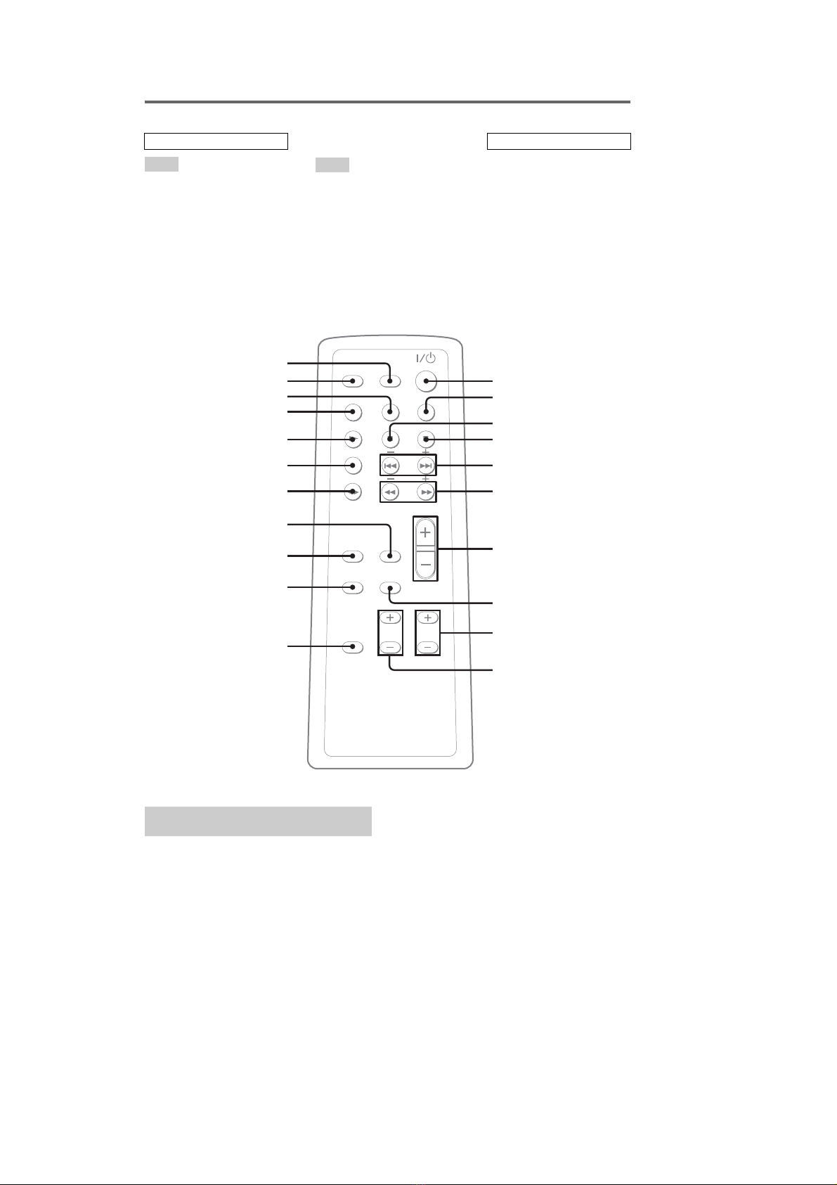
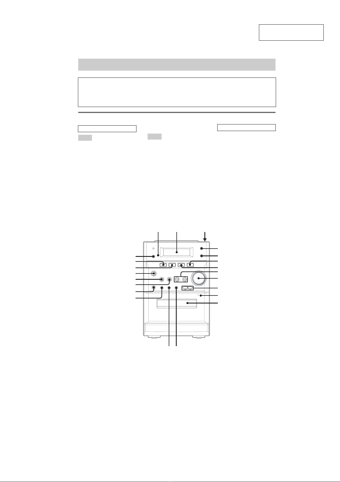
Sony SS-CEP515 User manual

CMT-EP515
US Model
Canadian Model
AEP Model
UK Model
E Model
SERVICE MANUAL
MICRO HI-FI COMPONENT SYSTEM
Sony Corporation
Home Audio Company
Published by Sony Engineering Corporation
9-877-155-02
2003G16-1
© 2003.07
•CMT-EP515 is composed of following model.
Asfortheservicemanual,itisissuedforeachcomponent
model, then, please refer to it.
Ver 1.1 2003. 07
COMPONENT MODEL NAME
HCD-EP515
SS-CEP515
Part No. Description Remarks
ACCESSORIES
************
1-754-243-11 ANTENNA (FM)
1-754-102-22 ANTENNA, LOOP (AM)
3-027-153-11 LID, BATTERY CASE (FOR RM-SGP5)
4-246-169-11 MANUAL, INSTRUCTION (ENGLISH)(US,CND,AEP,UK)
4-246-169-21 MANUAL, INSTRUCTION (FRENCH)(CND)
4-246-169-31 MANUAL, INSTRUCTION (FRENCH,SPANISH)(AEP)
4-246-169-41 MANUAL, INSTRUCTION (GERMAN,DUTCH,ITALIAN,
SWEDISH,POLISH)(AEP)
4-246-169-51 MANUAL, INSTRUCTION (KOREAN)(KR)
A-4433-976-A COMMANDER, STANDARD (RM-SGP5)
PARTS LIST
COMPACT DISC DECK
RECEIVER SYSTEM
SPEAKER SYSTEM
•Abbreviation
CND : Canadian model
KR : Korean model

HCD-EP515
US Model
Canadian Model
AEP Model
UK Model
E Model
SERVICE MANUAL
MICRO HI-FI COMPONENT SYSTEM
Sony Corporation
Home Audio Company
Published by Sony Engineering Corporation
9-877-160-03
2003G16-1
© 2003.07
HCD-EP515 is the Amplifier, CD player, Tape
Deck and Tuner section in CMT-EP515.
SPECIFICATIONS
Ver 1.2 2003. 07
Model Name Using Similar Mechanism NEW
CD CD Mechanism Type KSM-213EDP
Section Base Unit Name BU-K7BD44B
Optical Pick-up Name KSS-213E/C2N
TAPE Model Name Using Similar Mechanism NEW
Section Tape Transport Mechanism Type CMAL1Z240A
CD player section
System Compact disc and digital
audio system
LaserSemiconductor laser
(
λ
=780 nm)
Emission duration:
continuous
Frequency response 2 Hz – 20 kHz (±0.5 dB)
Tape deck section
Recording system 4-track 2-channel stereo
Frequency response 50 – 13,000 Hz (±3 dB),
using Sony TYPE I
cassettes
Amplifier section
AUDIO POWER SPECIFICATIONS:
(U.S.A. model only)
POWER OUTPUT AND TOTAL HARMONIC
DISTORTION:
With 6-ohm loads, both channels driven, from 120 -
10,000 Hz; rated 14 watts per channel minimum RMS
power, with no more than 10% total harmonic
distortion from 250 milliwatts to rated output.
North American model:
Continuous RMS power output (reference):
15 + 15 W
(6 ohms at 1 kHz, 10%
THD)
European model:
DIN power output (rated): 11 + 11 W
(6 ohms at 1 kHz, DIN)
Continuous RMS power output (reference):
15 + 15 W
(6 ohms at 1 kHz, 10%
THD)
Music power output (reference):
25 + 25 W
Other models:
The following measured at AC 230 V or AC 120 V, 50/
60 Hz
DIN power output (rated): 11 + 11 W
(6 ohms at 1 kHz, DIN)
Continuous RMS power output (reference):
15 + 15 W
(6 ohms at 1 kHz, 10%
THD)
Inputs
MD IN (phono jacks): Sensitivity 800 mV,
impedance 47 kilohms
Outputs
PHONES (stereo minijack):
Accepts headphones with
animpedance of 8 ohms or
more
SPEAKER: Accepts impedance of 6 to
16 ohms.
— Continued on next page —

2
HCD-EP515
1. SERVICING NOTES ······················································· 3
2. GENERAL ·········································································· 5
3. DISASSEMBLY
3-1. Rear Cabinet ··································································· 7
3-2. CD Cabinet Section, Front Panel Section ······················· 8
3-3. CD Mechanism Deck (KSM-213EDP)··························· 8
3-4. CONTROL Board, BACK LIGHT Board ······················ 9
3-5. Tape Mechanism Deck (CMAL1Z240A) ······················· 9
3-6. Cassette Door Assy ······················································· 10
3-7. POWER Board, MAIN Board ······································ 10
3-8. Optical Pick-up (KSS-213E/C2N) ································ 11
4. MECHANICAL ADJUSTMENTS ····························· 12
5. ELECTRICAL ADJUSTMENTS ······························· 13
6. DIAGRAMS······································································ 15
6-1. Block Diagram – CD Section – ··································· 17
6-2. Block Diagram – Main Section – ································ 18
6-3. Printed Wiring Board – CD Section – ························· 19
6-4. Schematic Diagram – CD Section – ···························· 20
6-5. Printed Wiring Borads – Main Section – ····················· 21
6-6. Schematic Diagram – Main Section – ························· 22
6-7. Printed Wiring Board – Control Section –··················· 23
6-8. Schematic Diagram – Control Section –······················ 24
6-9. Printed Wiring Board – Power Section – ·····················25
6-10. Schematic Diagram – Power Section –······················ 25
6-11. IC Pin Function Description ······································· 28
7. EXPLODEDVIEWS
7-1. Cabinet Section ····························································· 30
7-2. Front Panel Section ······················································· 31
7-3. CD Cabinet Section ······················································ 32
7-4. Optical Pick-up Block (KSM-213EDP) ······················· 33
8. ELECTRICAL PARTS LIST ······································· 34
TABLE OF CONTENTS
General
Power requirements
North American model: 120 V AC, 60 Hz
European model: 230 V AC, 50/60 Hz
Other models: 230 V AC, 50/60 Hz
Power consumption
North American model: 50 watts
European model: 50 watts
0.3 watts (in the standby
mode)
Other models: 50 watts
Dimensions (w/h/d) Approx. 163 × 233 × 237
mm
Mass Approx. 3.6 kg
Supplied accessories Remote (1)
R6 (size AA) batteries (2)
AM loop antenna (1)
FM lead antenna (1)
Design and specifications are subject to change
without notice.
Tuner section
FM stereo, FM/AM superheterodyne tuner
FM tuner section
Tuning range 87.5 – 108.0MHz(50-kHz
step)
Antenna FM lead antenna
Antenna terminals 75 ohms balanced
Intermediate frequency 10.7 MHz
AM tuner section
Tuning range
Pan-American model: 530 – 1,710 kHz
(with the tuning interval
set at 10 kHz)
531 – 1,602 kHz
(with the tuning interval
set at 9 kHz)
European model: 531 – 1,602 kHz
(with the tuning interval
set at 9 kHz)
Antenna AM loop antenna, external
antenna terminal
Intermediate frequency 450 kHz
Other models: 530 – 1,710 kHz
(with the tuning interval
set at 10 kHz)
531 – 1,602 kHz
(with the tuning interval
set at 9 kHz)
Ver 1.2 2003. 07

3
HCD-EP515
SECTION 1
SERVICING NOTES
Fig. A. Using an AC voltmeter to check AC leakage.
1.5 k
Ω
0.15
µ
FAC
voltmete
r
(0.75 V)
To Exposed Metal
Parts on Set
Earth Ground
SAFETY CHECK-OUT
After correcting the original service problem, perform the following
safety check before releasing the set to the customer:
Check the antenna terminals, metaltrim, “metallized” knobs, screws,
and all other exposed metal parts forAC leakage.
Check leakage as described below.
LEAKAGE TEST
The AC leakage from any exposed metal part to earth ground and
from all exposed metal parts to any exposed metal part having a
return to chassis, must not exceed 0.5 mA (500 microamperes.).
Leakage current can be measured by any one of three methods.
1. A commercial leakage tester, such as the Simpson 229 or RCA
WT-540A. Follow the manufacturers’instructions to use these
instruments.
2. A battery-operated AC milliammeter. The Data Precision 245
digital multimeter is suitable for this job.
3. Measuringthevoltagedropacrossaresistor by means of aVOM
or battery-operatedAC voltmeter. The “limit” indication is 0.75
V, so analog meters must have an accurate low-voltage scale.
The Simpson 250 and Sanwa SH-63Trd are examples of a
passiveVOM that is suitable. Nearly all battery operated digital
multimeters that have a 2VAC range are suitable. (See Fig.A)
CAUTION
Use of controls or adjustments or performance of procedures
other than those specified herein may result in hazardous
radiation exposure.
This appliance is classified as a CLASS 1 LASER product.
The CLASS 1 LASER PRODUCT MARKING is located on
the exterior.
Laser component in this product is capable of emitting radiation
exceeding the limit for Class 1.
The laser diode in the optical pick-up block may suffer electrostatic
break-down because of the potential difference generated by the
charged electrostatic load, etc. on clothing and the human body.
During repair, pay attention to electrostatic break-down and also
use the procedure in the printed matter which is included in the
repair parts.
The flexible board is easily damaged and should be handled with
care.
NOTES ON LASER DIODE EMISSION CHECK
The laser beam on this model is concentrated so as to be focused on
the disc reflective surface by the objective lens in the optical pick-
up block. Therefore, when checking the laser diode emission,
observe from more than 30 cm away from the objective lens.
LASER DIODE AND FOCUS SEARCH OPERATION
CHECK
Carry out the “S curve check” in “CD section adjustment”and check
that the S curve waveforms is output three times.
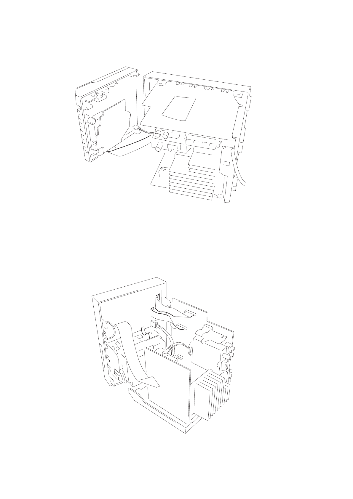
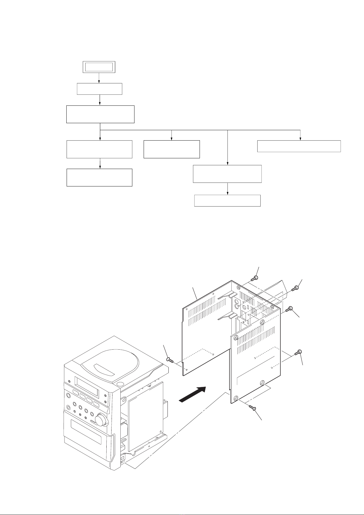
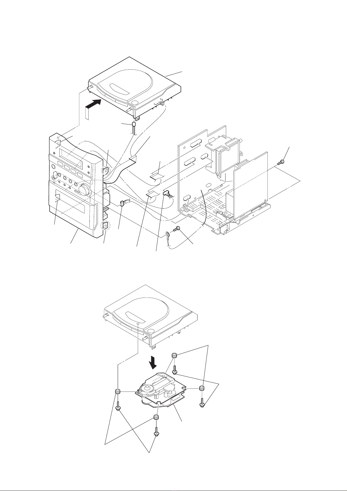
NOTES ON HANDLING THE OPTICAL PICK-UP
BLOCK OR BASE UNIT
Notes on chip component replacement
•Never reuse a disconnected chip component.
•Notice that the minus side of a tantalum capacitor may be dam-
aged by heat.
Flexible Circuit Board Repairing
•Keep the temperature of the soldering iron around 270 ˚C during
repairing.
•Do not touch the soldering iron on the same conductor of the
circuit board (within 3 times).
•Be careful not to apply force on the conductor when soldering or
unsoldering.
SAFETY-RELATED COMPONENT WARNING!!
COMPONENTS IDENTIFIED BY MARK 0OR DOTTED LINEWITH
MARK 0ON THE SCHEMATIC DIAGRAMS AND IN THE PARTS
LIST ARE CRITICAL TO SAFE OPERATION. REPLACE THESE
COMPONENTS WITH SONY PARTS WHOSE PART NUMBERS
APPEAR AS SHOWN IN THIS MANUAL OR IN SUPPLEMENTS
PUBLISHED BY SONY.
ATTENTION AU COMPOSANT AYANT RAPPORT
À LA SÉCURITÉ!
LES COMPOSANTS IDENTIFÉS PAR UNE MARQUE 0SUR LES
DIAGRAMMES SCHÉMATIQUES ET LA LISTE DES PIÈCES SONT
CRITIQUES POUR LA SÉCURITÉ DE FONCTIONNEMENT. NE
REMPLACER CES COMPOSANTS QUE PAR DES PIÈSES SONY
DONT LES NUMÉROS SONT DONNÉS DANS CE MANUEL OU
DANS LES SUPPÉMENTS PUBLIÉS PAR SONY.

4
HCD-EP515
Service Position of the CD Mechanism Deck
Service Position of theTape Cassette Mechanism Deck

5
HCD-EP515
SECTION 2
GENERAL This section is extracted
from instruction manual.
Main unit
BASS/TREBLE 5(13)
Cassette compartment qs
CD SYNC qd (12)
DIRECTION qg (11, 12, 15)
DISPLAY ws (9, 10, 16)
Display window 2
DSG 4(13)
MD 6(17)
PHONES jack qh
PLAY MODE qg (6, 7)
PRESET +/– 8(9)
Remote sensor 1
TUNER BAND w; (8, 9)
TUNING +/– 0(8, 9)
VOLUME 9(14, 15)
?/1 (power) ql (5, 9, 14, 15)
m/M (fast forward/rewind)
0(6, 11)
./> (go back/go forward)
8(5, 6, 7, 12, 13, 14, 15)
x(stop) qj (6, 7, 11, 12, 19)
X(pause) qk (6, 11)
zREC PAUSE/START qf (12,
15)
CD N(play) wa (6, 7)
TAPE nN (play) 7(11, 12,
15)
Z PUSH OPEN/CLOSE (CD
open/close) 3(6)
Z PUSH OPEN/CLOSE (tape
open/close) qa (11)
List of button locations and reference pages
How to use this page
Use this page to find the location of buttons and other
parts of the system that are mentioned in the text.
Ill
us
t
ra
ti
on num
b
er
r
DISPLAY ws (9, 10, 16)
RR
Name of button/part Reference page
ALPHABETICAL ORDER
A – M P – Z
BUTTON DESCRIPTIONS
12 3
4
5
6
7
8
9
q;
qa
qs
qdqf
qg
qh
qj
qk
ql
w;
wa
ws

6
HCD-EP515
1
Press ?/1to turn on the system.
2
Press CLOCK/TIMER SET.
3
Press ./
./
>repeatedly to set the
hour.
4
Press CLOCK/TIMER SET.
5
Press ./
./
>repeatedly to set the
minute.
6
Press CLOCK/TIMER SET.
The clock starts working.
To adjust the clock
1
Press CLOCK/TIMER SET.
2
Press ./> to select “CLOCK”, then
press CLOCK/TIMER SET.
3
Do the same procedures as step 3 to 6
above.
Setting the clock
Remote control
BASS +/– 0(13)
CLEAR 8(8, 9)
CLOCK/TIMER SELECT w;
(14, 15)
CLOCK/TIMER SET wa (5, 14,
15)
DISPLAY 2(9, 10, 16)
DSG qa (13)
MD qk (17)
PLAY MODE/DIRECTION qd
(6, 7, 11, 12, 15)
PRESET +/– 5(9)
REPEAT/FM MODE qf (7, 9)
SLEEP ql (13)
TREBLE +/– 9(13)
TUNER BAND qh (8, 9)
TUNER MEMORY qs (8)
TUNING +/– 6(8, 9)
VOL +/– 7(14, 15)
?/1 (power) 1(5, 9, 14, 15)
m/M (fast forward/rewind)
6(6, 11)
./> (go back/go forward)
5(5, 6, 7, 12, 14, 15)
x(stop) 4(6, 7, 11, 12, 19)
X(pause) 3(6, 11)
CD N(play) qj (6, 7)
TAPE nN (play) qg (11, 12,
15)
ALPHABETICAL ORDER
A – M P – Z
BUTTON DESCRIPTIONS
1
wa
w;
ql
qk
qj
qh
qg
qf
qd
qs
qa
2
3
4
5
6
7
8
9
0

7
HCD-EP515
SECTION 3
DISASSEMBLY
Note: Follow the disassembly procedure in the numerical order given.
• This set can be disassembled in the order shown below.
3-1. Rear Cabinet
REAR CABINET
CD MECHANISM DECK
(KSM-213EDP)
OPTICAL PICK-UP
(KSS-213E/C2N)
CONTROL BOARD,
BACK LIGHT BOARD POWER BOARD , MAIN BOARD
TAPE MECHANISM DECK
(CMAL1Z240A)
CASSETTE DOOR ASSY
SET
CD CABINET SECTION,
FRONT PANEL SECTION
1
two screws
(+BVTP 3
×
10)
3
two screws
(+BVTP 3
×
10)
4
two screws
(+BVTP 3
×
10
)
2
four screws
(+BVTP 3
×
10)
5
two screws
(+K 3
×
5)
6
two screws
(+K 3
×
5)
7
rear cabinet

8
HCD-EP515
3-2. CD Cabinet Section, Front Panel Section
3-3. CD Mechanism Deck (KSM-213EDP)
8
connector
(CN301)
q;
screw
(+BVTP 3
×
10)
qa
two screws
(+BVTP 3
×
10
)
1
connector
(S800)
9
connector
(CN307)
qf
front panel section
5
CD cabinet section
4
claw
3
claw
qs
claw
qd
claw
2
w
ire (flat type)
21p (CN101)
6
w
ire (flat type)
20p (CN303)
7
w
ire (flat type)
15p (CN302)
1
two screws
(+PWH 2.6
×
10)
4
two vibration proof rubbers (GRN)
5
CD mechanism deck
(KSM-213EDP)
3
two vibration proof rubbers (PNK
)
2
two screws
(+PWH 2.6
×
10)

9
HCD-EP515
3-4. CONTROL Board, BACK LIGHT Board
3-5.Tape Mechanism Deck (CMAL1Z240A)
1
knob volume
4
CONTROL board
7
BACK LIGHT board
2
four screws
(+BVTP 3
×
10)
3
five screws
(+BVTP 3
×
10
)
5
Remove the soldering.
6
two
claws
1
w
ire (flat type) 8p
2
three screws
(+BVTP 3
×
10
)
3
tape mechanism deck
(CMAL1Z240A)

10
HCD-EP515
3-6. Cassette Door Assy
3-7. POWER Board, MAIN Board
1
Open the cassette door assy.
3
cassette door assy
claw
2
1
connector
(AC IN)
2
connector
(CN901)
5
two screws
(+BVTP 3
×
10)
3
four screws
(+BVTP 4
×
12)
6
MAIN board
4
POWER board

11
HCD-EP515
3-8. Optical Pick-up (KSS-213E/C2N)
2
gear (A)
1
claw
5
sled shaft
6
KSS-213E/C2N
4
3

12
HCD-EP515
3.04 – 6.96 mN • m
(31 to 71 g • cm)
(0.43 – 0.98 oz • inch)
0.20 – 0.58 mN • m
(2 to 6 g • cm)
(0.02 – 0.08 oz • inch)
3.04 – 6.96 mN • m
(31 to 71 g • cm)
(0.43 – 0.98 oz • inch)
0.20 – 0.58 mN • m
(2 to 6 g • cm)
(0.02 – 0.08 oz • inch)
6.97 – 14.02 mN • m
(71 to 143 g • cm)
(0.98 – 1.99 oz • inch)
9.8 mN • m or more
(100 g • cm or more)
(1.4 oz • inch or more)
9.8 mN • m or more
(100 g • cm or more)
(1.4 oz • inch or more)
CQ-102C
CQ-102C
CQ-102RC
CQ-102RC
CQ-201B
CQ-403A
CQ-403R
Precaution
1. Clean the following parts with a denatured alcohol-moistened
swab:
record/playback heads pinch rollers
erase head rubber belts
capstan idlers
2. Demagnetize the record/playback head with a head demag-
netizer.
3. Do not use a magnetized screwdriver for the adjustments.
4. After the adjustments, apply suitable locking compound to the
parts adjusted.
5. The adjustments should be performed with the rated power
supply voltage unless otherwise noted.
Torque Measurement
SECTION 4
MECHANICAL ADJUSTMENTS
Mode
FWD
FWD
back tension
REV
REV
back tension
FF/REW
FWD tension
REV tension
Torque meter Meter reading

13
HCD-EP515
RFDC signal waveform
Checking Location: CD board (Conductor side)
RFAC Level Check
Connection:
Procedure:
1. Connect an oscilloscope to test point TP (RFAC) and TP (VC)
on the CD board.
2. Turn the power on.
3. Put the disc (YEDS-18) in to playback the number five track.
4. Confirm that oscilloscope waveform is clear and check RFAC
signal level is correct or not.
Note: A clear RFAC signal waveform means that the shape “◊” can be
clearly distinguished at the center of the waveform.
RFAC signal waveform
Checking Location: CD board (Conductor side) (See page 14)
CD SECTION
Note:
1. CD Block is basically designed to operate without adjustment. There-
fore, check each item in order given.
2. UseYEDS-18 disc (3-702-101-01) unless otherwise indicated.
3. Use an oscilloscope with more than 10MΩimpedance.
4. Clean the object lens by an applicator with neutral detergent when the
signal level is low than specified value with the following checks.
S-curve Check
Connection:
Procedure:
1. Connect an oscilloscope to test point TP (FE) and TP (DVC)
on the CD board.
2. Turn the power on.
3. Put the disc (YEDS-18) in and turned power switch on again
and actuate the focus search. (actuate the focus search when
disc table is moving in and out)
4. Check the oscilloscope waveform (S-curve) is symmetrical
betweenA and B.And confirm peak to peak level within 2 ± 1
Vp-p.
S-curve waveform
Note: •Try to measure several times to make sure than the ratio ofA : B
or B : A is more than 10 : 7.
•Take sweep time as long as possible and light up the
brightness to obtain best waveform.
Checking Location: CD board (Conductor side)
RFDC Level Check
Connection:
Procedure:
1. Connectanoscilloscopeto test pointTP (RFDC) andTP (DVC)
on the CD board.
2. Turn the power on.
3. Put the disc (YEDS-18) in to playback the number five track.
4. Confirm that oscilloscope waveform is clear and check RFDC
signal level is correct or not.
Note: A clear RFDC signal waveform means that the shape “◊” can be
clearly distinguished at the center of the waveform.
+
–
CD board
TP (FE)
TP (DVC)
oscilloscope
A
B
symmetry
within 2
±
1 Vp-p
+
–
CD board
TP (RFDC)
TP (DVC)
oscilloscope
VOLT/DIV: 200 mV
TIME/DIV: 500 ns
level: 1.15
±
0.35 Vp-p
+
–
CD board
TP (RFAC)
TP (VC)
oscilloscope
VOLT/DIV: 200 mV
TIME/DIV: 500 ns
level: 1.35
±
0.4 Vp-p
SECTION 5
ELECTRICAL ADJUSTMENTS

14
HCD-EP515
Checking Location:
– CD BOARD (Conductor Side) –
TP (VC)
TP (FE)
TP (TE)
TP
(RFDC)
TP
(DVC)
TP
(RFAC)
IC103
IC101

15
HCD-EP515
SECTION 6
DIAGRAMS
• Circuit Boards Location
THIS NOTE IS COMMON FOR PRINTEDWIRING
BOARDS AND SCHEMATIC DIAGRAMS.
(In addition to this,the necessary note is printed
in each block.)
For schematic diagrams.
Note:
•All capacitors are in µF unless otherwise noted. pF: µµF
50 WV or less are not indicated except for electrolytics
and tantalums.
•All resistors are in Ωand 1/4W or less unless otherwise
specified.
•f: internal component.
•2: nonflammable resistor.
•1: fusible resistor.
•C: panel designation.
For printed wiring boards.
Note:
•X: parts extracted from the component side.
•Y: parts extracted from the conductor side.
•f: internal component.
•: Pattern from the side which enables seeing.
•A: B+ Line.
•B: B– Line.
•VoltagesaretakenwithaVOM(Input impedance 10 MΩ).
Voltage variations may be noted due to normal produc-
tion tolerances.
•Waveforms are taken with a oscilloscope.
Voltage variations may be noted due to normal produc-
tion tolerances.
•Circled numbers refer to waveforms.
•Abbreviation
CND : Canadian model
•Signal path.
F: TUNER
J: CD
d: AUX
E: PB (TAPE)
a: REC (TAPE)
Note:
The components identified by
mark 0or dotted line with mark
0are critical for safety.
Replace only with part number
specified.
Note:
Les composants identifiés par
une marque 0sont critiques
pour la sécurité.
Ne les remplacer que par une
pièceportantle numéro spécifié.
CD board
MAIN board
REGULATOR board
BACK LIGHT board
POWER board
CONTROL board
HEADPHONE board

16
HCD-EP515
•Waveforms
– CD Board –
1.1Vp-p
1IC103 qg (RFAC)
(CD Play Mode)
2IC101 el (FE)
(CD Play Mode)
200mV/DIV,
1
µ
s
/DIV
50mV/DIV,
200
µ
s
/DIV
100mV/DIV,
200
µ
s
/DIV
1V/DIV,
20ns
/DIV
200mVp-p
250mVp-p
3IC101 ra (TE)
(CD Play Mode)
4IC101 yj (XTAO)
5.4Vp-p
59ns
6
IC801 qh (CF2)
1V/DIV,
40ns
/DIV
1V/DIV,
10
µ
s
/DIV
5
IC801 qd (XT2)
4.8Vp-p
30.5
µ
s
4.0Vp-p
116ns
7
Q307
collector (Rec mode)
5V/DIV,
4
µ
s
/DIV
11.3Vp-p
12.3
µ
s
– CONTROL Board – – MAIN Board –

1717
HCD-EP515
6-1. Block Diagram – CD Section –
: CD
• Signal Path
SQSO
SQCK
A/D
CONVERTER
CH1OUTF
CH1OUTR
6
7
8
9
16
18
11
10
12
2
1
51
49
48
43
24
41
40 39
64 15
28
29
30
31
32
33
24
25
23
5
6
2
3
17
18
15
16
E
B
C
D
A
CD +5V
F
DETECTOR
A
B
C
D
RF
SUMMING
AMP
FOCUS
ERROR AMP
TRACKING
ERROR AMP
RFAC
FE
IC103
RF AMP,
FOCUS/TRACKING ERROR AMP
TE
E
FF I-V AMP
E I-V AMP
Q101
AUTOMATIC
POWER
CONTROL
APC LD
AMP
LD
LD
PD
LASER DIODE
RFAC
ASYO
ASYI
ASYMMETRY
CORRECTION DIGITAL
PLL
IC101 (1/2)
DIGITAL SIGNAL PROCESSOR,
DIGITAL FILTER, D/A CONVERTER
DATA
XLAT
CLOK
14 56
MDP
26 7 8
XLON
3
XRST
DIGITAL
CLV
D/A
INTERFACE
SE
TE
FE
RFDC
FOCUS/TRACKING/SLED
SERVO DSP
FOCUS/TRACKING/SLED
PWM GENERATOR
SFDR
CH3FIN
CH4SIN
CH3RIN
CH3OUTF
CH3OUTR
CH2FIN
CH2RIN
CH1FIN
CH1RIN
20
MUTE
SRDR
TFDR
TRDR
FFDR
FRDR
S101
(LIMIT)
EMPH
WFCK
GFS
MIRR/DFCT/
FOK
DETECTOR
SERVO AUTO
SEQUENCER SERVO
INTERFACE
CPU INTERFACE
18
63
62
61
19
SENS
20
32
33
31
36 27
SCOR
CD SQSO
CD SQCK
CD XLT
CD CLK
CD DATA
CD SENS
CD SCOR
1 2
37 35
SCLK
COUT
921
SSTP
27
FOK
22
23
MIRR
DFCT
TO SERVO INTERFACE
CH4OUTF
CH4OUTR
(SPINDLE) MOTOR
DRIVE
MOTOR
DRIVE
CH2OUTF
CH2OUTR
M
M
(SLED)
IC102
FOCUS/TRACKING COIL DRIVE,
SPINDLE/SLED MOTOR DRIVE
2-AXIS
DEVICE
(TRACKING)
(FOCUS)
IC101 (2/2)
DIGITAL SERVO
PROCESSOR
OPTICAL PICK-UP
BLOCK
KSM-213EDP
SW
PD
I-V AMP
12
11
13
14
54 56 53 55
FILTER
FILO
PCO
CLTV
FILI
EFM
DEMODULATOR
SERIAL
IN
INTERFACE
DIGITAL
FILTER,
NOISE SHAPER
PWM
&
INTEGRATOR BUFFER
CLOCK
GENERATOR TIMING
LOGIC
DIGITAL
OUT
INTERNAL BUS
16K
RAM
ERROR
CORRECTOR
SUBCODE
PROCESSOR
60
92 CD XRST
XTAI
X101
16.9344MHz
AIN1
AIN2
AOUT1
AOUT2
TO MIRR/DFCT/
FOK DETECTOR
PCMD
BCK
LRCK
C2PO
DOUT
66
XTAO 67
70
77
LOUT1
LOUT2 R-CH
72
75
71
76 A
MAIN SECTION
EQ
IN 15
3
4EQ
AC
SUM
17
FEI
RF DC
AMP 28
RFDCO
29
RFDCI
COIL
DRIVE
COIL
DRIVE
10
9
CD PWM2
CD PWM1
PWM3
PWM2
PWM3
PWM2
93 CD LDON
IC801 (1/2)
CD
L-CH
RFAC
VCA
+7V
+7V
+5V
SYSTEM CONTROLLER
+3.3V
REG
Q102
CD +5V
REG
Q317

1818
HCD-EP515
6-2. Block Diagram – Main Section –
: TUNER
: CD
• Signal Path
: AUX
: PB (TAPE)
: REC (TAPE)
• R-CH is omitted due to same as L-CH.
BIAS
OSC
Q307
+10V
ERASE
HEAD
REC/PB
HEAD
DECK
TU DI
4
TU CLK
5
TU CE
6
SYSTEM CONTROLLER
IC801
TU DO
3
L
R
MD
J303
J301
PHONES
R CH
L
R
FUCTION
KEY
REMOTE
CONTROL
RECEIVER
IC802
S801-809
TUNER PACK
L-CH
R-CH R-CH
D OUT
D IN
CLK
CE
TUNED
R-CH
TU TUNED
87
REC/PB
SWITCH
Q326-332
T301
BIAS OSC
Q308
TA REC/PB
30
TA BIAS
98
TA SW
24
XT1
12
XT2
13
X801
32.768kHz
CF1
15
CF2
16
X802
8.64MHz
99
AMP MUTE
29
RMC
FUCTION
KEY
S810-817
20
KEY1
VOL
ENCODER
RV801
22
VOL ENCODER
2
MD LED
31
RESET
SWITCH
Q806
11
RESET RESET
IC803
13
23
I POWER DOWN
D907-910
RELAY
DRIVE
AC
IN
CD POWER
CONTROL
Q320
Q311 RY901
19
KEY0
34
CD ON
+5V
PB/REC EQ AMP
IC302
AUX L
19 18
OUT L
TU L
23
TAPE L
2
CD L
21
16
OUT R R-CH
13
CONT
28
REC OUT
TU MUTE
1
RDS DATA
7
TU STEREO
38
STEREO
MUTE
R DATA
R INT RDS CLK
26
R-CH
R-CH
L-CH
F DATA
91
TA PLAY SW
39
TA MOTOR
88
TA END SW
8
TA SOL
28
CD OPEN/CLOSE
94 CD OPEN
POWER
AMP
R CH
J302
SPEAKER
SEG1
SEG33
83
86
COM0
COM3
FLUORESCENT
DISPLAY
LCD801
POWER
CONTROL
D810
µCON +B
+5.6V (SUB)
D811
18
I POWER MONITOR
Q315
LINE
FILTER
LF901
+7V
REG
Q319
+7V
IC302
+5V
+5V
Q309
14
6 5
2
IC303
97
AMP STBY
12
D809
µCON +B
+10V
REG
IC305
13
D916-919
D911-914
+5V
REG
Q305
TU +5V +5V
REG
Q310
+10V
D319-321
POWER AMP
VCC
AC
DET
Q333
IC302
-5V -5V
REG
Q306
POWER
MONITER
Q338
+5.6V
REG
Q312-314
+10V
D317
95
POWER ON
+5.6V( SUB)
Q809
MECHANISM BLOCK
SW1
PLAY
T SOL
DRIVE
Q321,322
MOTOR
DRIVE
Q323,325
SW2
R REC
SW3
F REC
SW4
PACK
SW5
T END
M
M1
DECK
MOTOR
45
53
56
79
.
41
TA LED
42
TU LED
43
CD LED
40
ST/BY
96
BL ON
LED
DRIVE
Q801-805 D802-806
LED
DRIVE
Q808
D701-703
(BACK RIGHT)
R-CH
L OUT2
L OUT1
A
CD SECTION
S800
(OPEN)
(MAIN)
+5V +5V
REG
Q339 T902
POWER
(MAIN)
TRANSFORMER
T901
POWER
(SUB)
TRANSFORMER
Table of contents
Other Sony Stereo System manuals

Sony
Sony CPF-IX001 - Wireless PC-Linked Audio System Use and care manual

Sony
Sony GTK-XB60 User manual

Sony
Sony CMT-EP707 (CMTEP707) User manual

Sony
Sony MHC-G101 Primary User manual

Sony
Sony MHC-EC55 User manual

Sony
Sony SRS-X5 User manual

Sony
Sony MHC-GNX60 User manual

Sony
Sony RDP-X200iPN User manual

Sony
Sony HCD-ZX70DVD User manual

Sony
Sony Psyc ZS-YN7 User manual

Sony
Sony CMTBX1 - CMT BX1 Micro System User manual

Sony
Sony SA-PSD5 User manual

Sony
Sony HCD-CP101 User manual

Sony
Sony CMT-BX3 User manual

Sony
Sony SS-CEX100 User manual

Sony
Sony DHC-AZ33D User manual

Sony
Sony SA-WMS556 User manual

Sony
Sony SRS-X5 User manual

Sony
Sony ZS-X1 - Cd Boombox User manual

Sony
Sony FST-ZUX999 User manual