SERVICE MANUAL
COMPACT DISC DECK RECEIVER
US Model
Canadian Model
AEP Model
UK Model
Australian Model
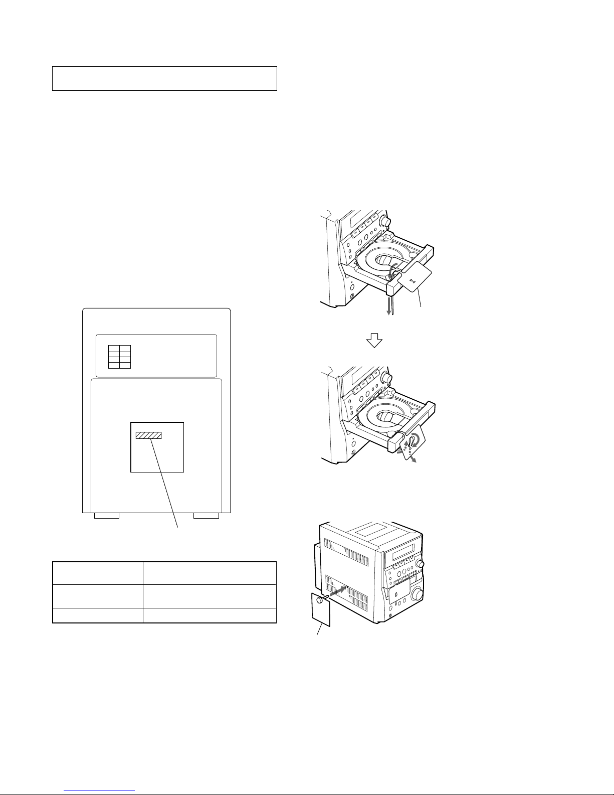
HCD-EP707
Ver 1.5 2003.08
HCD-EP707 is the amplifier, CD
player, tape deck and tuner section
in CMT-EP707.
SPECIFICATIONS
CD Model Name Using Similar Mechanism NEW
Section CD Mechanism Type CMCJ-0132
TAPE Model Name Using Similar Mechanism HCD-EP505
Section Tape Transport Mechanism Type CRL4349
9-874-043-06 Sony Corporation
2003H05-1 Home Audio Company
C2003.08 Published by Sony Engineering Corporation
CD player section
System Compact disc and digital
audio system
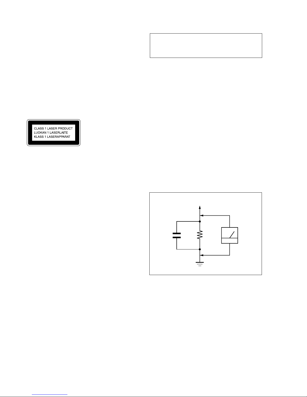
Laser Semiconductor laser
(λ=780 nm)
Emission duration:
continuous
Frequency response 20 Hz - 20 kHz (±0.5 dB)
OPTICAL DIGITAL OUT
(Square optical connector jack, rear panel)
Wavelength 660 nm
Tape player section
Recording system 4-track 2-channel stereo
Frequency response 50 - 13 000 Hz (±3 dB),
using Sony TYPE I
cassette
Tuner section
FM stereo, FM/AM superheterodyne tuner
FM tuner section
Tuning range 87.5 - 108.0 MHz
Antenna FM lead antenna
Antenna terminal (Except for European model)
75 Ωcoaxial
Intermediate frequency 10.7 MHz
AM tuner section
Tuning range
Pan-American model: 530 - 1 710 kHz
(with the interval set at
10 kHz)
531 - 1 710 kHz
(with the interval set at
9 kHz)
European model: 531 -1 602 kHz
(with the interval set at
9 kHz)
AUDIO POWER SPECIFICATIONS:
(U.S.A. model only)
POWER OUTPUT AND TOTAL
HARMONIC DISTORTION:
with 4 Ωloads both channels driven, from 120
- 10,000 Hz; rates 15 W per channel minimum
RMS power, with no more than 10% total
harmonic distortion from 250 mW to rated
output.
Amplifier section
Canadian model:
Continuous RMS power output (reference)
15 + 15 W
(4 Ωat 1 kHz, 10% THD)
European model:
DIN power output (rated) 12 + 12 W
(4 Ωat 1 kHz, DIN)
Continuous RMS power output (reference)
15 + 15 W
(4 Ωat 1 kHz, 10% THD)
Music power output (reference)
38 + 38 W
Other model:
The following measured at AC 230 V or AC 120 V,
50/60 Hz
DIN power output (rated) 12 + 12 W
(4 Ωat 1 kHz, DIN)
Continuous RMS power output (reference)
15 + 15 W
(4 Ωat 1 kHz, 10% THD)
Inputs
MD IN (phono jacks): voltage 450 mV,
impedance 47 kilohms
Outputs
PHONES: Accepts headphones of
(stereo mini jack) 8 Ωor more
SPEAKER: Accepts impedance of 8 to
16 Ω
General
Power requirements
North American model : 120 V AC, 60 Hz
Other models: 230 V AC, 50/60 Hz
Power consumption
European model: 38 W
0.5 W (in the standby
mode)
Other models: 38 W
Dimensions (w/h/d):
Approx. 180 ×246 ×335 mm
Mass: Approx. 5.0 kg
Supplied accessories: AM loop antenna (1)
Remote Commander (1)
Batteries (2)
FM lead antenna (1)
(Except for European
model)
Design and specifications are subject to change
without notice.
Other models: 531 - 1 602 kHz
(with the interval set at
9 kHz)
530 - 1 710 kHz
(with the interval set at
10 kHz)
Antenna AM loop antenna
Intermediate frequency 450 kHz