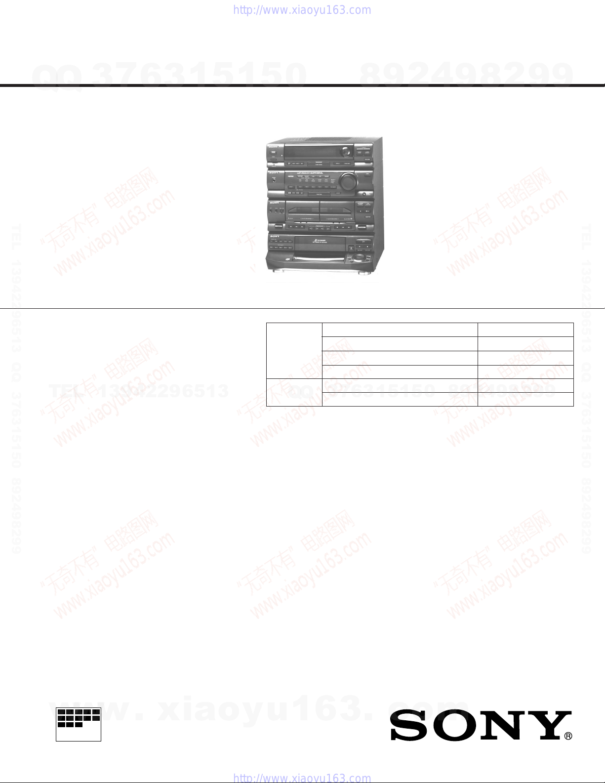
Sony HCD-N555AVK User manual

— 1 —
SERVICE MANUAL
MICROFILM
COMPACT DISC DECK RECEIVER
E Model
Model Name Using Similar Mechanism HCD-N355/N355K
CD Mechanism type CDM37-5BD19
Base Unit Type BU-5BD19
Optical Pick-up type KSS-213BA/S-N
Model Name Using Similar Mechanism HCD-N355/N355K
Tape Transport Mechanism Type TCM-220WR2E
HCD-N555AVK
TAPE
DECK
SECTION
* Manufactured under license from Dolby Laboratories
Licensing Corporation.
DOLBY, the double-D symbol aand “PRO LOGIC”
are trademarks of Dolby Laboratories Licensing Corpo-
ration.
SPECIFICATIONS
AM tuner section
Tuning range
Saudi Arabia model:
MW: 531-1,602 kHz (with the MW tuning interval set at 9 kHz)
SW: 5.95-17.90 MHz
Other models:
AM: 531-1,602 kHz (with the AM tuning interval set at 9 kHz)
530-1,710 kHz (with theAM tuning interval set at 10 kHz)
Aerial AM loop aerial
External aerial
terminals
Intermediate frequency
450 kHz
CD
SECTION
– Continued on next page –
CD player section
System Compact disc and
digital audio system
Laser Semiconductor laser
(λ=780nm)
Emission duration:
continuous
laser output Max 44.6 µW*
* This output is the value measured at a distance of 200 mm from the objec-
tive lens surface on the Optical Pick-up Block with 7 mm aperture.
Frequency response 2 Hz-20 kHz (± 0.5 dB)
Wavelength 780-790 nm
Tuner section
FM stereo, FM/AM superheterodyne tuner
FM tuner section
87.5-108.0 MHz (50 kHz step)
Aerial FM wire aerial
Aerial terminals 75 ohm unbalanced
Intermediate frequency
10.7 MHz
HCD-N555AVK is the tuner, deck, CD
and amplifier section in LBT-N555AVK.
w
w
w
.
x
i
a
o
y
u
1
6
3
.
c
o
m
Q
Q
3
7
6
3
1
5
1
5
0
9
9
2
8
9
4
2
9
8
T
E
L
1
3
9
4
2
2
9
6
5
1
3
9
9
2
8
9
4
2
9
8
0
5
1
5
1
3
6
7
3
Q
Q
TEL 13942296513 QQ 376315150 892498299
http://www.xiaoyu163.com

— 2 —
Tape player section
Recording system
4-track 2-channel stereo
Frequency response
40-13,000 Hz (±3 dB), using
SONY TYPE I cassette
40-14,000 Hz (±3 dB), using
SONY TYPE II cassette
Wow and flutter
± 0.15% W.Peak (IEC)
0.1% W.RMS (NAB)
± 0.2% W.Peak (DIN)
Amplifier section
Peak music power output:
1,400 W (6 a t 1 kHz, 10% THD)
Continuous RMS power output:
FRONT SPEAKER
45 W + 45 W (6 ohms, at 1 kHz, 5% THD)
SUPER WOOFER
45 W + 45 W (6 ohms, 5% THD)
SURROUND CENTER SPEAKER
40 W (8 ohms, at 1kHz 5% THD)
SURROUND REAR SPEAKER
20 W + 20 W (16 ohms, at 1 kHz, 5% THD)
Inputs
PHONO (phono jack):
Sensitivity 3 mV, impedance 47 kilohms
LD/VIDEO (AUDIO) (phono jack):
Sensitivity 250 mV, impedance 47 kilohms
MIC (phone jack):
Sensitivity 1 mV, impedance 10 kilohms
Outputs
PHONES (phone jack):
accept headphones of 6 to 16 ohms
FRONT SPEAKER: accept impedance of 6 to 16 ohms
SURROUND SPEAKER CENTER:
accept impedance of 8 to 16 ohms
SURROUND SPEAKER REAR:
accept impedance of 16 ohms
SUPER WOOFER:
accept impedance of 6 to 16 ohms
General
Power requirements
Malaysia model:
220-240 V AC, 50/60 Hz
Other models:
110-120 V or 220-240 V AC
adjustable, 50/60 Hz
Power consumption
240 W
Dimensions
Approx. 355 x 425 x 400 mm (w/h/d)
incl. projecting parts and controls
Mass
Approx. 13 kg
Design and specifications subject to change without notice.
Laser component in this product is capable of emitting radiation
exceeding the limit for Class 1.
This appliance is classified as a
CLASS 1 LASER product.
TheCLASS 1LASER PRODUCT
MARKING is located on the rear
exterior.
Notes on chip component replacement
• Never reuse a disconnected chip component.
• Notice that the minus side of a tantalum capacitor may be
damaged by heat.
Flexible Circuit Board Repairing
• Keep the temperature of soldering iron around 270˚C
during repairing.
• Do not touch the soldering iron on the same conductor of the
circuit board (within 3 times).
• Be careful not to apply force on the conductor when soldering
or unsoldering.
CAUTION
Use of controls or adjustments or performance of
procedures other than those specified herein may result in
hazardous radiation exposure.
Thiscaution label
is located inside
the unit.
SAFETY-RELATED COMPONENTWARNING !!
COMPONENTS IDENTIFIED BY MARK !OR DOTTED LINE
WITH MARK !ON THE SCHEMATIC DIAGRAMS AND IN
THE PARTS LIST ARE CRITICAL TO SAFE OPERATION.
REPLACE THESE COMPONENTS WITH SONY PARTS
WHOSE PART NUMBERS APPEAR AS SHOWN IN THIS
MANUAL OR IN SUPPLEMENTS PUBLISHED BY SONY.
w
w
w
.
x
i
a
o
y
u
1
6
3
.
c
o
m
Q
Q
3
7
6
3
1
5
1
5
0
9
9
2
8
9
4
2
9
8
T
E
L
1
3
9
4
2
2
9
6
5
1
3
9
9
2
8
9
4
2
9
8
0
5
1
5
1
3
6
7
3
Q
Q
TEL 13942296513 QQ 376315150 892498299
http://www.xiaoyu163.com

— 3 —
SERVICING NOTE
NOTES ON HANDING THE OPTICAL PICK-UP BLOCK
OR BASE UNIT
The laser diode in the optical pick-up block may suffer electrostatic
break-down because of the potential difference generated by the
charged electrostatic load, etc. on clothing and the human body.
During repair, pay attention to electrostatic break-down and also use
the procedure in the printed matter which is included in the repair
parts.
The flexible board is easily damaged and should be handled with
care.
NOTES ON LASER DIODE EMISSION CHECK
The laser beam on this model is concentrated so as to be focused on
the disc reflective surface by the objective lens in the optical pick-up
block. Therefore, when checking the laser diode emission, observe
from more than 30 cm away from the objective lens.
FL DisplayTube, LED All Lit and Key Check mode
When the TUNER/BAND , DISPLAY/DEMO , and FILE 2 but-
tons are pressed simultaneously, the FL display tube and LEDs will
all light up. Press any button to enter the key check mode.
When the key check mode is entered, the FL display tube displays
“K 1 J0 V0”. Each time a button is pressed, the counter increases in
the following order, K 2 nK 3 nK 4.
If buttons already pressed once are pressed again, the counter will
not increase. When the VOLUME knob is rotated in the + direction,
the count increases in the following order.
V1 nV2 nV3.
When rotated in the – direction, it decreases in the following order.
V0 nV9 nV8.
When the AMS dial is rotated in the clockwise direction, the count
increases in the following order.
J1 nJ2 nJ3.
When rotated in the counterclockwise direction, it decreases in the
following order.
J0 nJ9 nJ8.
To exit form the test mode, press the TUNER/BAND , DISPLAY/
DEMO , FILE 2 buttons simultaneously again.
How to switch LD/VIDEO which is the function name of
external input
The LD/VIDEO display which is the function name of external input
is set to "LD" on shipment. The display can be changed as below:
When the power is turned off, pressing the POWER and FUNC-
TION buttons simultaneously, "VIDEO" is displayed on the FL dis-
play tube. In this operation, the function name of external input is
switched to "VIDEO". Turn the power off in the same way, pressing
the POWER and FUNCTION buttons simultaneously again, "LD"
is displayed on the FL display tube. In this operation, the function
name of external input is switched to "LD". The function names of
external input can be changed at will by the way of the above.
How to reset all
Pressing the TUNER/BAND , DISPLAY/DEMO and FILE 3 buttons
simultaneously , all are reset and returned to as when the unit was
shipped.
Switching the channel step 9 kHz/10 kHz
Press ENTER/NEXT button and POWER button simultaneously
to switch the AM channel step 9 kHz and 10 kHz. Be sure not to
change with carelessness.
MODEL
E, Indonesian model
Saudi Arabia model
Singapore (SP2) model
Singapore (SP4) model
Malaysia model
PARTS No.
4-978-194-5π
4-978-194-6π
4-978-194-7π
4-978-194-8π
4-978-194-9π
Parts No.
NOTE: The difference between SP2 and SP4 is the back panel only.
MODEL IDENTIFICATION
– BACK PANEL –
123456789
1
2345678
9
123456789
9
w
w
w
.
x
i
a
o
y
u
1
6
3
.
c
o
m
Q
Q
3
7
6
3
1
5
1
5
0
9
9
2
8
9
4
2
9
8
T
E
L
1
3
9
4
2
2
9
6
5
1
3
9
9
2
8
9
4
2
9
8
0
5
1
5
1
3
6
7
3
Q
Q
TEL 13942296513 QQ 376315150 892498299
http://www.xiaoyu163.com

— 4 —
6. EXPLODED VIEWS
6-1. Case and Back Panel Section ............................................... 88
6-2. Panel Board Section ............................................................. 89
6-3. Front panel Section .............................................................. 90
6-4. Chassis Section .................................................................... 91
6-5. TC Mechanism Section 1 (TCM-220WR2E) ...................... 92
6-6. TC Mechanism Section 2 (TCM-220WR2E) ...................... 93
6-7. TC Mechanism Section 3 (TCM-220WR2E) ...................... 94
6-8. CD Mechanism Section(CDM37-5BD19)........................... 95
6-9. Base Unit Section (BU-5BD19)........................................... 96
7. ELECTRICAL PARTS LIST ......................................... 97
• Abbreviation
EA : Saudi Arabia model
SP : Singapore model
MY : Malaysia model
IA : Indonesian model
TABLE OF CONTEMTS
1. GENERAL ............................................................................ 5
2. DISASSEMBLY
2-1. Front Panel Assembly, Main Board and Key Con Board....... 7
2-2. TC Mechanism Deck ............................................................. 7
2-3. CD Mechanism Deck ............................................................. 8
2-4. BU Bracket Assy .................................................................... 8
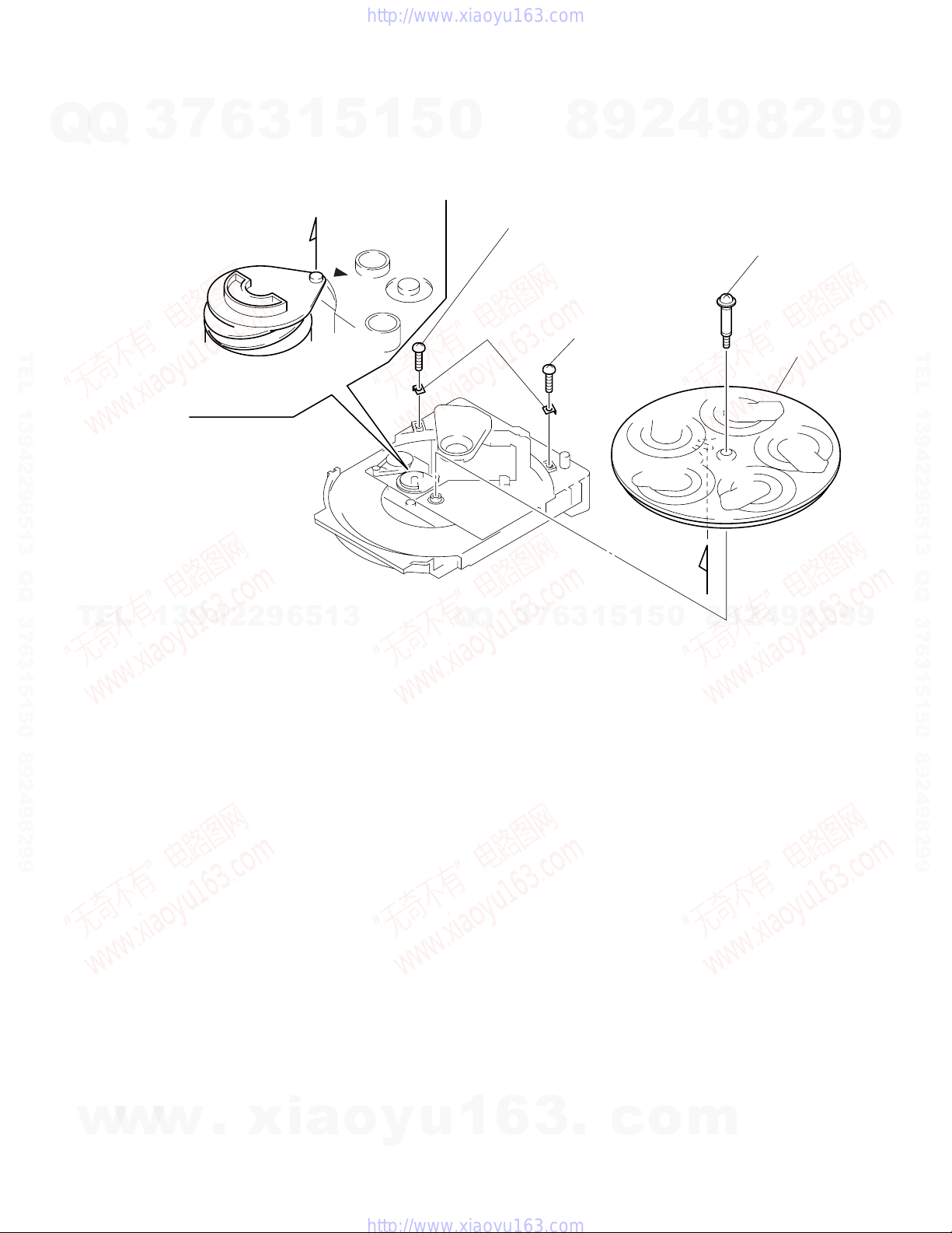
2-5. Disc Table .............................................................................. 9
3. MECHANICAL ADJUSTMENTS ........................... 10
4. ELECTRICAL ADJUSTMENTS
DECK Section ............................................................................. 10
TUNER Section........................................................................... 13
CD Section................................................................................... 15
5. DIAGRAMS
5-1. Circuit boards location ........................................................ 17
5-2. IC Pin Functions .................................................................. 18
• IC501 Graphic Control (ASD0204) .................................. 18
• IC701 Master Control (TMP87CS64YF) .......................... 19
5-3. Block Diagrams
• Main Section...................................................................... 22
• Tuner Section
(E, SP, MY, IA Model) ....................................................... 25
• Tuner Section
(EA Model) ........................................................................ 27
• DECK Section ................................................................... 29
• CD Section......................................................................... 31
5-4. Schematic Diagram — Tuner Section —
(E, SP, MY, IA Model) ......................................................... 34
5-5. Printed Wiring Board — Tuner Section —
(E, SP, MY, IA Model) ......................................................... 36
5-6. Schematic Diagram — Tuner Section —
(EA Model) ......................................................................... 38
5-7. Printed Wiring Board — Tuner Section —
(EA Model) ......................................................................... 40
5-8. Schematic Diagram — CD Panel Section — ...................... 41
5-9. Printed Wiring Board — CD Panel Section —.................... 42
5-10. Schematic Diagram — CD Section — .............................. 45
5-11. Printed Wiring Board — CD Section —............................ 47
5-12. Printed Wiring Board — Deck Section — ......................... 49
5-13. Schematic Diagram — Deck Section —............................ 51
5-14. Printed Wiring Board — Main Section — ......................... 57
5-15. Schematic Diagram — Main Section —............................ 59
5-16. Schematic Diagram — Panel Section — ........................... 64
5-17. Printed Wiring Board — Panel Section — ........................ 69
5-18. Printed Wiring Board — Power Section — ....................... 73
5-19. Schematic Diagram — Power Section — .......................... 77
5-20. Schematic Diagram — CD Motor Section — ................... 80
5-21. Printed Wiring Board — CD Motor Section —................. 81
5-22. Schematic Diagram — Key Control Section — ................ 83
5-23. Printed Wiring Board — Key Control Section —.............. 85
5-24. IC Block Diagrams — CD Section — ............................... 86
w
w
w
.
x
i
a
o
y
u
1
6
3
.
c
o
m
Q
Q
3
7
6
3
1
5
1
5
0
9
9
2
8
9
4
2
9
8
T
E
L
1
3
9
4
2
2
9
6
5
1
3
9
9
2
8
9
4
2
9
8
0
5
1
5
1
3
6
7
3
Q
Q
TEL 13942296513 QQ 376315150 892498299
http://www.xiaoyu163.com

— 7 —
1
Remove the connectors.
• Main board (six connectors)
• power amplifier board (one connector)
2-2.TC MECHANISM DECK
SECTION 2
DISASSEMBLY
Note: Follow the disassembly procedure in the numerical order given.
2-1. FRONT PANEL ASSEMBLY, MAIN BOARD AND KEY CON BOARD
2
Screw (BVTP3 X 8)
6
Screw (BVTP 3x8)
9
Key con board
6
Button (eject-L)
3
Three screws
(BVTP 2.6X8)
4
Four screws
(BVTP 2.6X8)
5
TC mechanism deck
7
Button (eject-R)
1
Push the eject button.
2
Remove the two cassette lids
direction of arrow.
CN1301
CN250
CN201
3
Two earth wire
7
Two screws
(BVTP 3X8)
8
Main board
CN701
CN203
CN402
CN401
Power amplifier board
5
Front panel assembly
4
Three screws
(BVTP 3X8)
w
w
w
.
x
i
a
o
y
u
1
6
3
.
c
o
m
Q
Q
3
7
6
3
1
5
1
5
0
9
9
2
8
9
4
2
9
8
T
E
L
1
3
9
4
2
2
9
6
5
1
3
9
9
2
8
9
4
2
9
8
0
5
1
5
1
3
6
7
3
Q
Q
TEL 13942296513 QQ 376315150 892498299
http://www.xiaoyu163.com

— 8 —
2-3. CD MECHANISM DECK
2-4. BU BRACKET ASSEMBLY
2
BU bracket assembly
1
Yoke bracket
1
Screw (BVTP 3x8)
2
Two screws
(BVTP 3x8)
4
CD mechanism
deck
3
Two screws
(BVTP 3x8)
w
w
w
.
x
i
a
o
y
u
1
6
3
.
c
o
m
Q
Q
3
7
6
3
1
5
1
5
0
9
9
2
8
9
4
2
9
8
T
E
L
1
3
9
4
2
2
9
6
5
1
3
9
9
2
8
9
4
2
9
8
0
5
1
5
1
3
6
7
3
Q
Q
TEL 13942296513 QQ 376315150 892498299
http://www.xiaoyu163.com

— 9 —
A
A
5
Disc table
4
Step screw
1
Screw (BVTP 3x8)
2
Screw (BVTP 3x8)
3
Bracket (BU)
2-5. DISCTABLE
Note:
When the Disc table is installed, adjust the positions
of Roller cam and mark (as shown in the figure,
then set to the groove of disc table.
w
w
w
.
x
i
a
o
y
u
1
6
3
.
c
o
m
Q
Q
3
7
6
3
1
5
1
5
0
9
9
2
8
9
4
2
9
8
T
E
L
1
3
9
4
2
2
9
6
5
1
3
9
9
2
8
9
4
2
9
8
0
5
1
5
1
3
6
7
3
Q
Q
TEL 13942296513 QQ 376315150 892498299
http://www.xiaoyu163.com

— 10 —
SECTION 3
MECHANICAL ADJUSTMENTS SECTION 4
ELECTRICAL ADJUSTMENTS
PRECAUTION
1. Clean the following parts with a denatured alcohol-moistened
swab :
record/playback heads pinch rollers
erase head rubber belts
capstan idlers
2. Demagnetize the record/playback head with a head demagnetizer.
3. Do not use a magnetized screwdriver for the adjustments.
4. The adjustments should be performed with the rated power sup-
ply voltage unless otherwise noted.
Torque Measurement
Torque
FWD
FWD
back tension
REV
REV
back tension
FWD tension
REV tension
FF/REW
Torque meter
CQ-102C
CQ-102C
CQ-102RC
CQ-102RC
CQ-201B
CQ-403A
CQ-403R
Meter reading
36 to 61g • cm
(0.5–0.84 oz • inch)
2 to 6g • cm
(0.02–0.08 oz • inch)
36 to 61g • cm
(0.5–0.84 oz • inch)
2 to 6g • cm
(0.02–0.08 oz • inch)
61 to 143g • cm
(0.85–1.99 oz • inch)
100g or more
(3.53 oz or more)
100g or more
(3.53 oz or more)
DECK SECTION 0 dB=0.775V
1. Demagnetize the record/playback head with a head damagnetizer.
2. Do not use a magnetized screwdriver for the adjustments.
3. After the adjustments, apply suitable locking compound to the
parts adjusted.
4. The adjustmetns should be performed with the rated power sup-
ply voltage unless otherwise noted.
5. The adjustments should be performed in the order given in this
service manual. (As a general rule, playback circuit adjustment
should be completed before performing recording circuit adjust-
ment.)
6. The adjustments should be performed for both L-CH and R-ch.
7. Switches and controls should be set as follows unless otherwise
specified.
Tape
P-4-A100
WS-48B
P-4-L300
Signal
10 kHz, –10 dB
3 kHz, 0 dB
315 Hz, 0 dB
Used for
Azimuth Adjustment
Tape Speed Adjustment
Level Adjustment
Record/Playback Head Azimuth Adjustment
DECK A DECK B
Note : Perform this adjustments for both decks.
Procedure :
1. Mode : Playback (FWD)
level meter
main board
CN403
Pin
3
(L-CH)
Pin
1
(R-CH)
test tape
P-4-A100
(10kHz, –10dB)
set
main board
CN403
Pin
2
w
w
w
.
x
i
a
o
y
u
1
6
3
.
c
o
m
Q
Q
3
7
6
3
1
5
1
5
0
9
9
2
8
9
4
2
9
8
T
E
L
1
3
9
4
2
2
9
6
5
1
3
9
9
2
8
9
4
2
9
8
0
5
1
5
1
3
6
7
3
Q
Q
TEL 13942296513 QQ 376315150 892498299
http://www.xiaoyu163.com

— 11 —
2. Turn the adjustment screw and check output peaks. If the peaks
do not match for L-CH and R-CH, turn the adjustment screw so
that outputs match within 1 dB of peak.
3. Mode : Playback (FWD)
test tape
P-4-A100
(10kHz, –10dB) main board
CN403
Pin
3
Pin
2
L
R
Pin
1
oscilloscope
Waveform of oscilloscope
good wrong
in phase 45° 90° 135° 180°
4. Repeat steps 1 to 3 in playback (REV) mode.
5. After the adjustments, apply suitable locking compound to the
parts adjusted.
Adjustment Location : Record/Playback Head (Deck A and B)
DeckA is RV311 (L-CH) and RV411 (R-CH), deck B is RV301 (L-
CH) and RV401 (R-CH) so that adjustment within the following ad-
justment level.
Adjustment level :
CN403 PB level : 301.5 to 338.3 mV (–8.2 to –7.2 dB)
level difference between the channels : within ± 0.5 dB
Adjustment Location : MD board
L-CH
peak
screw
position
R-CH
peak
within
1dB
output
level
R-CH
peak
L-CH
peak
within 1dB
screw
position
set
FWD side REV side
Adjustment screw
frequency counter
test tape
WS-48B
(3kHz, 0dB)
level meter
set
test tape
P-4-L300
(315Hz, 0dB)
main board
CN403 (Pin
3
: L-CH)
(Pin
1
: R-CH)
Tape Speed Adjustment DECK A
Note : Start the tape speed adjustment as bellow after setting the
test mode. The tape speed can be changed with the HIGH
SPEED DUBBING button during the test mode.
Method :
1. Turn the power switch on.
2. Press the DISPLAY/DEMO button, MENU 1 button and TUNER/
BAND button simulateously.
Procedure :
Mode : Playback (FWD)
1. Insert the WS-48B into the deck A to playback.
2. Press the HIGH SPEED DUBBING button. Then at HIGH
SPEED mode.
3. Adjust RV652 on the MD board so that the frequency counter
reading becomes 6,000 ± 30 Hz.
4. Press the HIGH SPEED DUBBING button again to be set the
NORMAL SPEED mode.
5. Set to the playback mode.
6. Adjust RV651 on the MD board so that the frequency counter
reading becomes 3,000 ± 15 Hz.
Frequency difference between deck A and deck B the beginning of
the tape should be within ± 1.5%.
Adjustment Location : MD board
Playback Level Adjustment DECK A DECK B
Procedure :
Mode : Playback (FWD)
main board
CN403 (Pin
3
: L-CH)
(Pin
1
: R-CH)
set
w
w
w
.
x
i
a
o
y
u
1
6
3
.
c
o
m
Q
Q
3
7
6
3
1
5
1
5
0
9
9
2
8
9
4
2
9
8
T
E
L
1
3
9
4
2
2
9
6
5
1
3
9
9
2
8
9
4
2
9
8
0
5
1
5
1
3
6
7
3
Q
Q
TEL 13942296513 QQ 376315150 892498299
http://www.xiaoyu163.com

— 12 —
LD/VIDEO IN
1) 315Hz
2) 10kHz 50mV (–23.8dB)
blank tape
CS-123
AF OSC
attenuator 600
set
Record Bias Current Adjustment DECK B
Procedure :
1. Mode : record
2. Mode : Playback
recorded
position
set
level meter
CN 403 (Pin
3
: L-CH)
(Pin
1
: R-CH)
Confirm playback the signal recorded in step 1 become adjustment
level as follows.
If these levels do not adjustment level, adjust the RV341 (L-CH) and
RV441 (R-CH) on the MD board to repeat step 1 and 2.
Adjustment level : The playback output of 10 kHz level difference
against 315Hz reference should be ± 0.5 dB
Adjustment Location : MD board
Record Level Adjustment DECK B
Procedure :
1. Mode : record
LD/VIDEO IN
315Hz, 50mV (–23.8dB)
AF OSC
attenuator 600 blank tape
CS-123
set
2. Mode : Playback
recorded
position
set
level meter
main board
CN403 (Pin
3
: L-CH)
(Pin
1
: R-CH)
Confirm playback the signal recorded in step 1 become adjustment
level as follows.
If these levels do not adjustment level, adjust the RV301 (L-CH) and
RV351 (R-CH) on the main board to repeat steps 1 and 2.
Adjustment level: CN 403 PB level: 47.2 to 53.0 mV
(–24.3 to –23.3 dB)
Adjustment Location : main board
Adjustment Location
[MAIN BOARD] (Component Side)
RV351RECLEVEL(R-CH)
RV301 REC LEVEL
(L-CH)
1
3
CN403
– DECK B –
RECORD
BIAS
L
RV441 RV341
(NORMAL)
RV651
¬
R
TAPE SPEED
PB
LEVEL
L
¬
R
¬
– DECK A –
PB LEVEL
RV301
¬
L
RV401
¬
R
[MD BOARD] (Conductor Side)
(HIGH)
RV652
¬
w
w
w
.
x
i
a
o
y
u
1
6
3
.
c
o
m
Q
Q
3
7
6
3
1
5
1
5
0
9
9
2
8
9
4
2
9
8
T
E
L
1
3
9
4
2
2
9
6
5
1
3
9
9
2
8
9
4
2
9
8
0
5
1
5
1
3
6
7
3
Q
Q
TEL 13942296513 QQ 376315150 892498299
http://www.xiaoyu163.com

— 13 —
Procedure :
1. Set the output of SSG so that the input level of the set becomes 55
dB.
2. Tune the set to 999 kHz or 1050 kHz .
3. Adjust RV41 (EA model), RV42 (other model) to the point
(moment) when the TUNED indicator will change from going off
to going on.
Adjustment Location : TCB board
FMTuned Level Adjustment
Note : This adjustment should be performed after the AM Tuned
Level Adjustement.
Setting :
Band : FM
Adjustment Location
EA model
[TCB BOARD] (Component Side)
loop antenna
(Supplied accessories)
AM RF SSG
30% amplitude
modulation by
400 Hz signal
AM antenna
terminal (TM1)
60 cm
Field strength dB (µV/m)=SGG output level dB (µV/m)–26dB.
Carrier frequency : 999kHz (at 9kHz step)
1050kHz (at 10 kHz step)
• Abbreviation
EA : Saudi Arabia model
75 coaxial
Carrier frequency : 98MHz
Modulation : AUDIO 1kHz, 75kHz
deviation (100%)
Output level : 25dB (at 75 open)
set
FM ANTENNA terminal
(TM1) (75 )
Procedure :
1. Supply a 25dB 98 MHz signal from the ANTENNA terminal.
2. Tune the set to 98 MHz.
3. Adjust RV42 (EA model), RV41 (other model) to the point
(moment) when the TUNED indicator will change from going off
to going on.
Adjustment Location : TCB board
TUNER SECTION 0dB=1µV
Note : As a front-end (FE1) is difficult to repair if faulty, replace it
with new one.
AMTuned Level Adjustment
Note : FM Tuned Level adjustment should be performed after this
AM Tuned Level adjustment.
Setting :
Band : AM or MW
loop antenna
RV41
IC41
RV42
RV42
FM Tuned Level
FE1
TM1
RV41
FM Tuned Level
IC2
RV41
RV42
AM Tuned Level
FE1
TM1
RV41
AM Tuned Level
RV42
FM RF SSG
Other model
[TCB BOARD] (Component Side)
w
w
w
.
x
i
a
o
y
u
1
6
3
.
c
o
m
Q
Q
3
7
6
3
1
5
1
5
0
9
9
2
8
9
4
2
9
8
T
E
L
1
3
9
4
2
2
9
6
5
1
3
9
9
2
8
9
4
2
9
8
0
5
1
5
1
3
6
7
3
Q
Q
TEL 13942296513 QQ 376315150 892498299
http://www.xiaoyu163.com

— 14 —
SW OSCVoltage Adjustment
(EA model)
Setting:
Band: SW
Procedure:
1. Connect digital Voltmeter to diode D1 center lead and ground.
2. Adjust for a following value reading on digital voltmeter.
SWTracking Adjustment
(EA model)
Setting:
Band: SW
Procedure:
Adjust for maximum reading on level meter.
SW
• Repeat the procedures is each adjustment several times, and the
frequency coverage and tracking adjustment should be finally done
by the trimmer capacitors.
Adjustment Location
[TCB BOARD] — Component Side —
• Abbreviation
EA : Saudi Arabia model
set
SPEAKER terminal
CV2 CV1
T2 T1
CV1, T1
SW Tracking
Adjustment
level meter
AM RF SSG
30% amplitude
modulation by
400Hz signal AM ANTENNA terminal
TM1
RV41
RV42
D1, CV2, T2
SW OSC Voltage
Adjustment
D1
IC41
Adjustment
part Reading on digital
voltmeter
SW 5.95 MHz
17.9 MHz
T2
CV2
1.2 ± 0.1 V
8.5 ± 0.2 V
7 MHz
17 MHz
T1
CV1
Set frequency
Set frequency Adjustment
part
w
w
w
.
x
i
a
o
y
u
1
6
3
.
c
o
m
Q
Q
3
7
6
3
1
5
1
5
0
9
9
2
8
9
4
2
9
8
T
E
L
1
3
9
4
2
2
9
6
5
1
3
9
9
2
8
9
4
2
9
8
0
5
1
5
1
3
6
7
3
Q
Q
TEL 13942296513 QQ 376315150 892498299
http://www.xiaoyu163.com

— 15 —
oscilloscope
(DC range)
BD board
Procedure :
1. Connect oscilloscope to test point TP (RF).
2. Turned Power switch on.
3. Put disc (YEDS-18) in and playback.
4. Adjust RV101 so that the waveform is clear.
(ClearRF signalwaveformmeansthat the shape “◊” can be clearly
distinguished at the center of the waveform.)
5. After adjustment, check the RF signal level.
• RF signal
VOLT/DIV : 200 mV
TIME/DIV : 500 nS
S Curve Check
BD board
TP(FEO)
TP(VC)
oscilloscope
Symmetry
within 2.4 ± 0.7 Vp-p
6. After check, remove the lead wire connected in step 2.
Note : • Try to measure several times to make sure than the ratio of
A : B or B :A is more than 10 :7.
• Take sweep time as long as possible and light up the
brightness to obtain best waveform.
RF Level Check
BD board
TP(RF)
TP(VC)
oscilloscope
Procedure :
1. Connect oscilloscope to test point TP (RF) on BD board.
2. Turned Power switch on.
3. Put disc (YEDS-18) in and playback.
4. Confirm that osilloscope waveform is clear and check RF signal
level is correct or not.
Note :
Clear RF signal waveform means that the shape“◊” can be clearly
distinguished at the center of the waveform.
RF signal waveform
VOLT/DIV : 200mV
TIME/DIV : 500nS
level : 1.3 ± 0.3 Vp-p
CD SECTION
Note :
1. CD Block is basically designed to operate without adjustment.
Therefore, check each item in order given.
2. UseYEDS-18 disc (3-702-101-01) unless otherwise indicated.
3. Use an oscilloscope with more than 10M impedance.
4. Clean the object lens by an applicatior with neutral detergent when
the signal level is low than specified value with the following
checks.
5. Adjust the focus bias adjustment when optical block is replaced.
Focus Bias Adjustment
TP(RF)
TP(VC)
Procedure :
1. Connect oscilloscope to test point TP (FEO).
2. Connect between test point TP (FOK) and Ground by lead wire.
3. Turn Power switch on.
4. Put disc (YEDS-18) in and turned Power switch on again and
actuate the focus search. (actuate the focus search when disc table
is moving in and out.)
5. Check the oscilloscope waveform (S-curve) is symmetrical
betweenA and B.And confirm peak to peak level within 2.4 ± 0.7
Vp-p.
S-curve waveform
level
1.3 ± 0.3 Vp-p
A
B
w
w
w
.
x
i
a
o
y
u
1
6
3
.
c
o
m
Q
Q
3
7
6
3
1
5
1
5
0
9
9
2
8
9
4
2
9
8
T
E
L
1
3
9
4
2
2
9
6
5
1
3
9
9
2
8
9
4
2
9
8
0
5
1
5
1
3
6
7
3
Q
Q
TEL 13942296513 QQ 376315150 892498299
http://www.xiaoyu163.com

— 16 —
E-F Balance Check
BD board
TP (TEO)
TP (VC)
oscilloscope
Procedure :
1. Connect test point TP703 (ADJ 2) on Main board to Ground with
a lead wire.
2. Connect oscilloscope to test point TP (TEO).
3. Turned Power switch on.
4. Put disc (YEDS-18) in and playback.
5. Confirm that the oscilloscope waveform is symmetrical on the
top and bottom in relation to 0Vdc, and check this level.
Traverse waveform
0V
level : 300 ± 100 mVp-p
Specified level : • X 100=less than ± 7%
• A+B=300 ± 100 mVp-p
6. Remove the lead wire connected in step 1.
Focus/Tracking Gain Adjustment (RV102, RV103)
This gain has a margin, so even if it is slightly off.
There is no problem.
Therfore, do not perform this adjustment.
Please note that it should be fixed to mechanical center position when
you moved and do not know original position.
A-B
2(A+B)
Adjustment Location :
[BD BOARD] (Conductor Side)
[MAIN BOARD] (Conductor Side)
RF FOK
RV101
RV103
IC101 IC102
TEI
FEI
TEO
RV102
VC
IC104
GND
PCK
IC701
B
A
FEO
TP703
(ADJ2)
w
w
w
.
x
i
a
o
y
u
1
6
3
.
c
o
m
Q
Q
3
7
6
3
1
5
1
5
0
9
9
2
8
9
4
2
9
8
T
E
L
1
3
9
4
2
2
9
6
5
1
3
9
9
2
8
9
4
2
9
8
0
5
1
5
1
3
6
7
3
Q
Q
TEL 13942296513 QQ 376315150 892498299
http://www.xiaoyu163.com

— 17 —
MAIN board
Note: pA is including in MD board.
SECTION 5
DIAGRAMS
5-1. CIRCUIT BOARDS LOCATION
CD LED board
HP board
PANEL board
CD (L) board
TRANS board
S.WOOFER board
TCB board
KEY CON board
POWER AMP board
CD (R) board
CD JOG board
DOOR SW board
TC CONTROL board
TC SW board
MIC board
LEAF SWITCH board
MD board (including
p
A)
p
A MOTOR board
BD board
LED board
TABLE SENSOR board
CD MOTOR board
w
w
w
.
x
i
a
o
y
u
1
6
3
.
c
o
m
Q
Q
3
7
6
3
1
5
1
5
0
9
9
2
8
9
4
2
9
8
T
E
L
1
3
9
4
2
2
9
6
5
1
3
9
9
2
8
9
4
2
9
8
0
5
1
5
1
3
6
7
3
Q
Q
TEL 13942296513 QQ 376315150 892498299
http://www.xiaoyu163.com

— 18 —
5-2. IC PIN FUNCTIONS
• IC501 GRAPHIC CONTROL (ASD0204)
Function
I/O
Pin Name
Pin No. VDD
LED8
LDE7, 6
LED5–1
RESET
X2
X1
IC (Vpp)
XT2
JOG B
VDD
LED10, 9
KEY SEL
VOL B
REQ. GM
CLK MG
DATA GM
DATA MG
AVSS
SPEANA 4–1
KEY 4–1
AVDD
AVREF
VOL A
JOG A
RDY MG
SIRCS
VSS
DOR SW
LED SELECT
LED13–11
VDD
LEDS7, 6
LEDS5, 4
LEDS3–1
SEG32–8
V, LOAD
SEG7–1
GR14–1
–
O
O
O
I
O
I
–
I
I
–
O
O
I
O
I
O
I
–
I
I
–
–
I
I
I
I
–
I
O
O
–
O
O
O
O
–
O
O
+5V
LED drive signal output.
Reset signal input.
X’ tal (4 MHz).
GND
Not used.
AMS encoder signal input.
+5V
LED drive signal output.
Key select control.
Volume encoder signal input.
Request signal from/to master control.
Serial clock input.
Serial data output.
Serial data input.
GND
Spectram analizer signal input.
Key matrix input.
+5V
Volume encoder signal input.
AMS encoder signal input.
Ready signal from master control.
SIRCS signal input.
GND
CD door open detection input.
LED select signal output.
LED drive signal output.
+5V
Not used.
LED drive signal output.
FL segment signal output.
–25V for FL
FL segment signal output.
FL grid signal output.
• Abbreviation
FL: Fluorescent Indicator Tube
GND: Ground
1
2
3, 4
5-9
10
11
12
13
14
15
16
17, 18
19
20
21
22
23
24
25
26-29
30-33
34
35
36
37
38
39
40
41
42
43-45
46
47, 48
49, 50
51-53
54-78
79
80-86
87-100
w
w
w
.
x
i
a
o
y
u
1
6
3
.
c
o
m
Q
Q
3
7
6
3
1
5
1
5
0
9
9
2
8
9
4
2
9
8
T
E
L
1
3
9
4
2
2
9
6
5
1
3
9
9
2
8
9
4
2
9
8
0
5
1
5
1
3
6
7
3
Q
Q
TEL 13942296513 QQ 376315150 892498299
http://www.xiaoyu163.com

— 19 —
VSS
XOUT
XIN
RESET
XOUT
XIN
GND (test)
AC CUT
SUPER WOOFER ON
ST-MUTE ON
180-A-PLAY
180-B-PLAY
180-B-REC
V. DET
BD-UP (5CD)
TRAY CLOSE (1CD)
ENCODER-1
ENCODER-2
ENCODER-3
OUT SW OPEN
LOAD IN
LOAD OUT
TBL-L
TBL-R
SCOR
TBL-SENS
RDS INT
RDS DATA
DF LAT
SENS
XRST
MG-RDY
ADJ
GM-REQ
MG-CLK
GM-DATA
MG-DATA
CD-CLK
ADJ-2
CD-DATA
• IC701 MASTER CONTROL (TMP87CS64YF)
Function
I/OPin Name
Pin No. –
O
I
I
O
I
–
I
O
O
I
I
I
I
I
I
I
I
I
I
O
O
O
O
I
I
I
I
O
I
O
O
I
I
O
I
O
O
I
O
GND
X’ tal (10 MHz)
Reset signal input.
X’ tal for clock (32.768 kHz)
GND
Back up signal input.
Super woofer ON/OFF control.
Mute signal output for tuner.
Tape detection sigal input. (Connected to GND)
Voltage detection (Not used).
Disc table up detect.
Connected to GND
Input selector control signal output. (Pull up)
Out switch signal input. (Pull up)
Loading motor control signal output. (Not used)
Table motor control signal output.
Sub-code sync signal input.
CD Table sensor signal input.
RDS data start input. (Not used)
RDS data output. (Not used)
Latch signal for digital filter.
Table sence signal input.
Reset signal output for CD.
Ready signal to graphic control.
Test mode input.
Request signal from graphic control.
Clock signal to graphic control.
Data input from graphic control.
Data output to graphic control.
Clock output. Serial bus line.
Test mode input.
Data output. Serial bus line.
1
2
3
4
5
6
7
8
9
10
11
12
13
14
15
16
17
18
19
20
21
22
23
24
25
26
27
28
29
30
31
32
33
34
35
36
37
38
39
40
• Abbreviation
FL : Fluorescent Indicator Tube
GND : Ground
w
w
w
.
x
i
a
o
y
u
1
6
3
.
c
o
m
Q
Q
3
7
6
3
1
5
1
5
0
9
9
2
8
9
4
2
9
8
T
E
L
1
3
9
4
2
2
9
6
5
1
3
9
9
2
8
9
4
2
9
8
0
5
1
5
1
3
6
7
3
Q
Q
TEL 13942296513 QQ 376315150 892498299
http://www.xiaoyu163.com

— 20 —
Function
I/OPin Name
Pin No.
AUB IN
AUB OUT
FOCUS SW
SQ-CLK
SQ-DATA
X-LAT
TEST
VAREF
AVSS
VSS
VDD
SPEC
DESTINATION
DISC SENS
TC RELAY
A-SHUT
B-SHUT
B-HALF
A-HALF
220-A-PLAY
220-B-PLAY
62427 LAT
K-CON-LAT
VOL LAT (AV)
FRONT SP RELAY B
REAR SP RELAY C
POWER ON
CD POWER
RPOLOG LAT
MUTE
COM CLK
COM DIN
COM DATA
K CON ON
LIDDED LED
MD/VIDEO
DBFB-HIGH
PWM-OUT
PRO-LOGIC
TC A
41
42
43
44
45
46
47
48
49
50
51
52
53
54
55
56
57
58
59
60
61
62
63
64
65
66
67
68
69
70
71
72
73
74
75
76
77
78
79
80
I
O
O
O
I
O
I
I
–
–
–
I
I
I
O
I
I
I
I
I
I
O
O
O
O
O
O
O
O
O
O
I
O
O
O
O
O
I
O
O
Audio bus in/output. (Not used)
Focus switching signal output.
Subcode Q data read clock output.
Subcode Q data input.
Latch signal digital signal processor.
Test land.
Analog reference voltage input.
GND
+5V
Destination detection input.
Not used.
REC/PB select signal output.
Control signal input form deck.
PLL latch output.
Latch signal for KEY CONTROL.
Latch signal for electrical volume. (Not used)
Not used.
Rear speaker relay control output.
Power on signal output
CD power control signal output.
Not used.
Mute signal for AMP.
PLL clock output. (PLL, Function, Graphic Equalizer)
PLL data input. (PLL, Function, Graphic Equalizer)
PLL data output. (PLL, Function, Graphic Equalizer)
Control signal output for KEY CONTROL.
Disc No. LED drive signal output.
MD/VIDEO select output.
DBFB switching signal output.
Not used.
Dolby pro-logic control ourput.
Deck A, B select output.
w
w
w
.
x
i
a
o
y
u
1
6
3
.
c
o
m
Q
Q
3
7
6
3
1
5
1
5
0
9
9
2
8
9
4
2
9
8
T
E
L
1
3
9
4
2
2
9
6
5
1
3
9
9
2
8
9
4
2
9
8
0
5
1
5
1
3
6
7
3
Q
Q
TEL 13942296513 QQ 376315150 892498299
http://www.xiaoyu163.com
Table of contents
Other Sony Stereo System manuals

Sony
Sony CAS-1 User manual

Sony
Sony HCD-GX750 - System Components User manual

Sony
Sony CMT-GP8D

Sony
Sony MHC-F150 - Mini Hi Fi System User manual

Sony
Sony SS-CEX5 User manual

Sony
Sony HCD-LV80 User manual

Sony
Sony MHC-V818 User manual

Sony
Sony CMT-GS30DAB User manual

Sony
Sony SRS-BTX500 User manual

Sony
Sony MHC-V90W Reference guide

Sony
Sony SRS-BTX300 User manual

Sony
Sony MHC-V71D User manual

Sony
Sony BKSR-2020 User manual

Sony
Sony MEX-N5000BT User manual

Sony
Sony MHC-V41D User manual

Sony
Sony LBT-LX5 User manual

Sony
Sony WHG-SLK1i - Audio System Component Setup guide

Sony
Sony CMT-GP6V User manual

Sony
Sony SHAKE5 Use and maintenance manual

Sony
Sony MHC-GX750 User manual