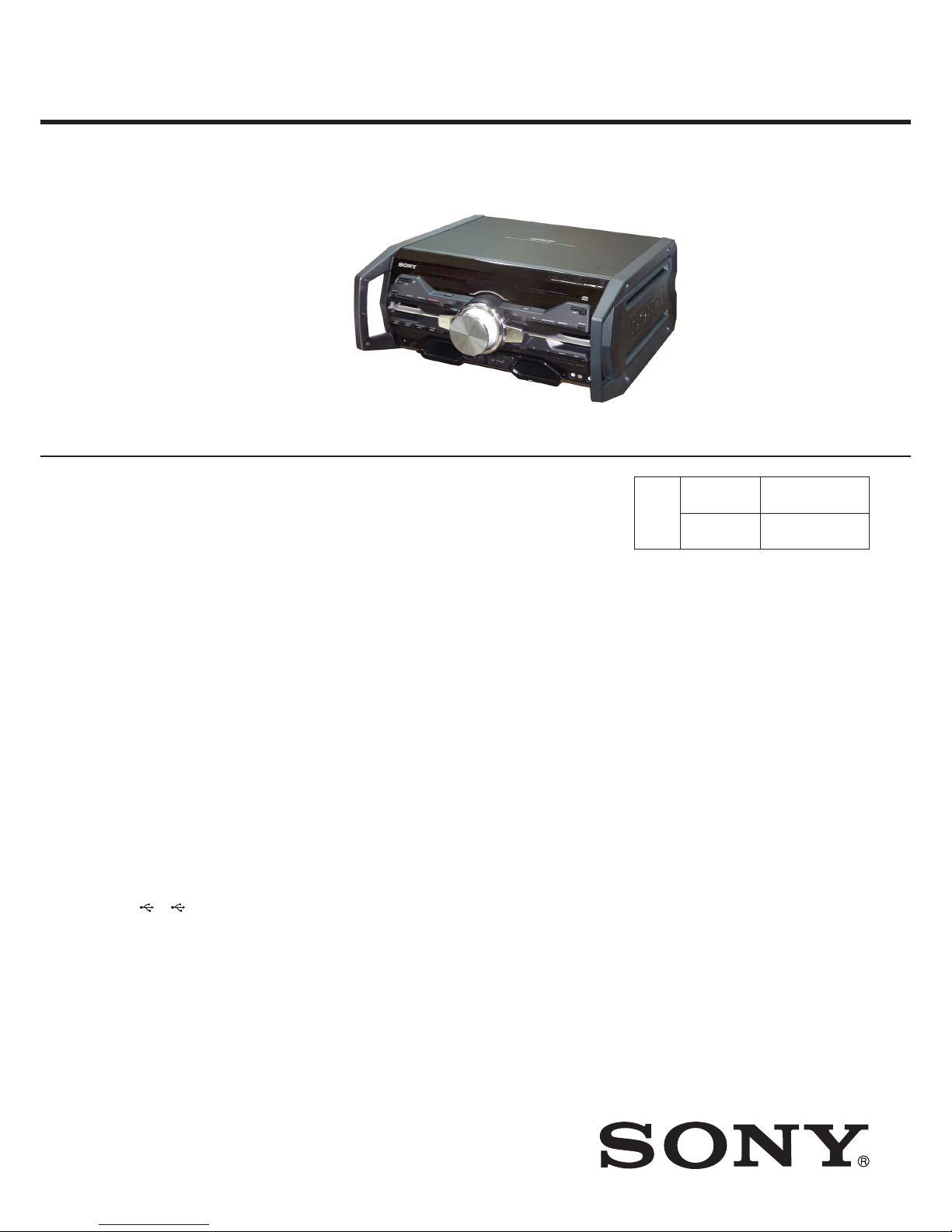
Sony HCD-SH2000 User manual

SERVICE MANUAL
Sony Corporation
Published by Sony EMCS (Malaysia) PG Tec
HCD-SH2000
MINI HI-FI COMPONENT SYSTEM
9-890-576-02
2011I08-1
© 2011.09
E Model
Ver. 1.1 2011.09
• HCD-SH2000 is the tuner, USB, CD
and amplifier section in FST-SH2000/LBT-SH2000.
• “WALKMAN” and “WALKMAN” logo are registered trademarks of Sony Corporation.
• MPEG Layer-3 audio coding technology and patents licensed from Fraunhofer IIS and
Thomson.
• Windows Media is either a registered trademark or trademark of Microsoft Corporation in
the United States and/or other countries.
• This product contains technology subject to certain intellectual property rights of Microsoft.
Use or distribution of this technology outside of this product is prohibited without the ap-
propriate license(s) from Microsoft.
SPECIFICATIONS
Amplifier section
The following are measured at AC 120 V -
240 V, 50/60 Hz
Power output (rated):
High channel
300 W + 300 W (at 4 Ω, 1 kHz,
1% THD)
Low channel
300 W + 300 W (at 4 Ω, 100 Hz,
1% THD)
RMS output power (reference):
High channel
500 W + 500 W (per channel at
4 Ω, 1 kHz)
Low channel
500 W + 500 W (per channel at
4 Ω, 100 Hz)
Inputs
PC (AUDIO IN) L/R, TV (AUDIO IN) L/R,
DVD/SAT (AUDIO IN) L/R, GAME
(AUDIO IN) L/R
Voltage 2 V, impedance 47 kΩ
MIC
Sensitivity 1 mV, impedance 10 kΩ
A, B port: Type A
USB section
Supported bit rate
MP3 (MPEG 1 Audio Layer-3):
32 kbps – 320 kbps, VBR
WMA: 48 kbps – 192 kbps
AAC: 48 kbps – 320 kbps
Sampling frequencies
MP3 (MPEG 1 Audio Layer-3):
32 kHz/44.1 kHz/48 kHz
WMA: 44.1 kHz
AAC: 44.1 kHz
Transfer speed
Full-Speed
Supported USB device
Mass Storage Class
Maximum current
500 mA
Disc player section
System
Compact disc and digital audio system
Laser Diode Properties
Emission Duration: Continuous
Laser Output*: Less than 44.6 μW
* This output is the value measurement
at a distance of 200 mm from the
objective lens surface on the Optical
Pick-up Block with 7 mm aperture.
Frequency response
20 Hz – 20 kHz
Signal-to-noise ratio
More than 90 dB
Dynamic range
More than 88 dB
Tuner section
FM stereo, FM/AM superheterodyne tuner
Antenna:
FM lead antenna
AM loop antenna
FM tuner section
Tuning range
87.5 MHz – 108.0 MHz (50 kHz step)
AM tuner section
Tuning range
AR, E2, E51 and MX models:
530 kHz – 1,710 kHz (10 kHz step)
531 kHz – 1,710 kHz (9 kHz step)
MY model:
530 kHz – 1,610 kHz (10 kHz step)
531 kHz – 1,602 kHz (9 kHz step)
General
Power requirements
AC 120 V – 240 V, 50/60 Hz
Power consumption
320 W
Dimensions (w/h/d) (excl. speakers)
(Approx.)
510 mm × 235 mm × 420 mm
Mass (excl. speakers) (Approx.)
10.0 kg
Supplied accessories
Remote control (1)
R6 (Size AA) batteries (2)
FM lead/AM loop antenna (1)
Speaker foot (8)
Design and specifications are subject to
change without notice.
• Abbreviation
E2 : 120V AC area in E model
E51 : Chilean and Peruvian models
EA : Saudi Arabia model
MX : Mexican model
MY : Malaysia model
SAF : South African model
CD
Section
CD Mechanism
Type CDM86B-DVBU101
Optical Pick-up
Name KHM-313CAB/C2NP

HCD-SH2000
2
SAFETY-RELATED COMPONENT WARNING!
COMPONENTS IDENTIFIED BY MARK 0OR DOTTED LINE
WITH MARK 0ON THE SCHEMATIC DIAGRAMS AND IN
THE PARTS LIST ARE CRITICAL TO SAFE OPERATION.
REPLACE THESE COMPONENTS WITH SONY PARTS
WHOSE PART NUMBERS APPEAR AS SHOWN IN THIS
MANUAL OR IN SUPPLEMENTS PUBLISHED BY SONY.
SAFETY CHECK-OUT
After correcting the original service problem, perform the following
safety check before releasing the set to the customer:
Check the antenna terminals, metal trim, “metallized” knobs,
screws, and all other exposed metal parts for AC leakage. Check
leakage as described below.
LEAKAGE TEST
The AC leakage from any exposed metal part to earth ground and
from all exposed metal parts to any exposed metal part having a
return to chassis, must not exceed 0.5 mA (500 microamperes).
Leakage current can be measured by any one of three methods.
1. A commercial leakage tester, such as the Simpson 229 or RCA
WT-540A. Follow the manufacturers’ instructions to use these
instruments.
2. A battery-operated AC milliammeter. The Data Precision 245
digital multimeter is suitable for this job.
3. Measuring the voltage drop across a resistor by means of a
VOM or battery-operated AC voltmeter. The “limit” indication
is 0.75 V, so analog meters must have an accurate low-voltage
scale. The Simpson 250 and Sanwa SH-63Trd are examples
of a passive VOM that is suitable. Nearly all battery operated
digital multimeters that have a 2V AC range are suitable. (See
Fig. A)
1.5 kΩ0.15 μF
AC
voltmeter
(0.75 V)
To Exposed Metal
Parts on Set
Earth Ground
Fig. A. Using an AC voltmeter to check AC leakage.

HCD-SH2000
3
1. SERVICING NOTES ............................................. 4
2. DISASSEMBLY
2-1. Side Panel A, Side Panel B and Top Panel Section ........ 6
2-2. Back Panel Section ......................................................... 7
2-3. Front Panel Section ........................................................ 7
2-4. DMB21 Board................................................................. 8
2-5. CDM Section .................................................................. 8
2-6. CD MECHANISM DECK BLOCK (1) ......................... 9
2-7. CD MECHANISM DECK BLOCK (2) ......................... 9
2-8. DAMP Board, MAIN Board........................................... 10
2-9. SWITCHING REGULATOR ......................................... 10
3. TEST MODE ............................................................ 11
4. ELECTRICAL CHECK ......................................... 13
5. DIAGRAMS
5-1. Block Diagram - RS SERVO, USB Section -................. 15
5-2. Block Diagram - MAIN Section -................................... 16
5-3. Block Diagram - AMP Section -..................................... 17
5-4. Block Diagram - PANEL, POWER SUPPLY Section - . 18
5-5. Printed Wiring Board
- MAIN Board (Component Side) (Suffix 11) -.............. 20
5-6. Printed Wiring Board
- MAIN Board (Conductor Side) (Suffix 11) - ............... 21
5-7. Printed Wiring Board
- MAIN Board (Component Side) (Suffix 12) - ............. 22
5-8. Printed Wiring Board
- MAIN Board (Conductor Side) (Suffix 12) - ............... 23
5-9. Schematic Diagram - MAIN Board (1/4) (Suffix 11) -... 24
5-10. Schematic Diagram - MAIN Board (2/4) (Suffix 11) -... 25
5-11. Schematic Diagram - MAIN Board (3/4) (Suffix 11) -... 26
5-12. Schematic Diagram - MAIN Board (4/4) (Suffix 11) -... 27
5-13. Schematic Diagram - MAIN Board (1/4) (Suffix 12) - .. 28
5-14. Schematic Diagram - MAIN Board (2/4) (Suffix 12) - .. 29
5-15. Schematic Diagram - MAIN Board (3/4) (Suffix 12) - .. 30
5-16. Schematic Diagram - MAIN Board (4/4) (Suffix 12) - .. 31
5-17. Printed Wiring Board
- DMB21 Board (Component Side) - ............................ 32
5-18. Printed Wiring Board
- DMB21 Board (Conductor Side) - ............................... 33
5-19. Schematic Diagram - DMB21 Board (1/3) - .................. 34
5-20. Schematic Diagram - DMB21 Board (2/3) - .................. 35
5-21. Schematic Diagram - DMB21 Board (3/3) - .................. 36
5-22. Printed Wiring Boards
- DAMP Board (Component Side) - ............................... 37
5-23. Printed Wiring Boards
- DAMP Board (Conductor Side) -................................. 38
5-24. Schematic Diagram - DAMP Board (1/4) - .................... 39
5-25. Schematic Diagram - DAMP Board (2/4) - .................... 40
5-26. Schematic Diagram - DAMP Board (3/4) - .................... 41
5-27. Schematic Diagram - DAMP Board (4/4) - .................... 42
5-28. Printed Wiring Boards - DISPLAY Board - ................... 43
5-29. Schematic Diagram - DISPLAY Board -........................ 44
5-30. Printed Wiring Boards - VOLUME Board- .................... 45
5-31. Schematic Diagram - VOLUME Board - ....................... 46
5-32. Printed Wiring Boards - BUTTON, USB Board -.......... 47
5-33. Schematic Diagram - BUTTON, USB Board - .............. 48
5-34. Printed Wiring Boards - VOLUME LED,
BOTTON LED AND TUNER Board -........................... 49
TABLE OF CONTENTS
5-35. Schematic Diagram - VOLUME LED,
BOTTON LED AND TUNER Board -........................... 50
5-36. Printed Wiring Boards - AUDIO-IN Board - ................. 51
5-37. Schematic Diagram - AUDIO-IN Board -...................... 51
5-38. Printed Wiring Boards - MIC Board - ............................ 52
5-39. Schematic Diagram - MIC Board -................................. 52
6. EXPLODED VIEWS
6-1. Main Section ................................................................... 65
6-2. Front Panel Section (1) ................................................... 66
6-3. Back Panel Section ......................................................... 67
6-4. Chassis Section ............................................................... 68
6-5. CDM Section .................................................................. 69
7. ELECTRICAL PARTS LIST .............................. 70

HCD-SH2000
4
SECTION 1
SERVICING NOTES
Notes on chip component replacement
• Never reuse a disconnected chip component.
• Notice that the minus side of a tantalum capacitor may be
damaged by heat.
Flexible Circuit Board Repairing
• Keep the temperature of the soldering iron around 270 °C
during repairing.
• Do not touch the soldering iron on the same conductor of the
circuit board (within 3 times).
• Be careful not to apply force on the conductor when soldering
or unsoldering.
UNLEADED SOLDER
Boards requiring use of unleaded solder are printed with the
leadfree mark (LF) indicating the solder contains no lead.
(Caution: Some printed circuit boards may not come printed with
the lead free mark due to their particular size)
: LEAD FREE MARK
Unleaded solder has the following characteristics.
• Unleaded solder melts at a temperature about 40 °C higher
than ordinary solder.
Ordinary soldering irons can be used but the iron tip has to be
applied to the solder joint for a slightly longer time.
Soldering irons using a temperature regulator should be set to
about 350 °C.
Caution: The printed pattern (copper foil) may peel away if
the heated tip is applied for too long, so be careful!
• Strong viscosity
Unleaded solder is more viscous (sticky, less prone to flow)
than ordinary solder so use caution not to let solder bridges
occur such as on IC pins, etc.
• Usable with ordinary solder
It is best to use only unleaded solder but unleaded solder may
also be added to ordinary solder.
CAUTION
Use of controls or adjustments or performance of procedures
other than those specified herein may result in hazardous radiation
exposure.
NOTES ON HANDLING THE OPTICAL PICK-UP BLOCK
OR BASE UNIT
The laser diode in the optical pick-up block may suffer electrostatic
break-down because of the potential difference generated by the
charged electrostatic load, etc. on clothing and the human body.
During repair, pay attention to electrostatic break-down and also
use the procedure in the printed matter which is included in the
repair parts.
The flexible board is easily damaged and should be handled with
care.
NOTES ON LASER DIODE EMISSION CHECK
The laser beam on this model is concentrated so as to be focused
on the disc reflective surface by the objective lens in the optical
pickup block. Therefore, when checking the laser diode emission,
observe from more than 30 cm away from the objective lens.
MODEL IDENTIFICATION
- BACK PANEL -
This appliance is
claassified as a CLASS 1
LASER product. This
label is located on the
rear exterior.
Model Part No.
E2, E51, EA, MY, SAF 4-275-656-0[]
MX 4-275-656-1[]
• Abbreviation
E2 : 120 V AC area in E model
E51 : Chilean and Peruvian models
EA : Saudi Arabian model
MX : Mexican model
MY : Malaysia model
SAF : South African model
PLAYABLE DISC
Format of discs Logo
• AUDIO CD
• CD-R/-RW in AUDIO
CD format
• CD-R/-RW in DATA CD
format, containing MP3
audio tracks
1) that
conforms to ISO 9660 2)
Level 1/Level 2, Joliet
(in expansion format), or
Multi Session
3)
1) MP3 (MPEG 1 Audio Layer 3) is a standard format defined
by ISO/MPEG which compresses audio data. MP3 audio
tracks must be in MPEG 1 Audio Layer 3 format.
2) A logical format of files and folders on CD-ROMs, defined
by ISO (International Organization for Standardization).
3) This is a recording method that enables adding of data using
the Track-At-Once method. Conventional discs begin at a
disc control area called the Lead-in and end at an area called
Lead-out. A Multi Session disc is a disc having multiple
sessions, with each segment from Lead-in to Lead-out
regarded as a single session.
NOTE OF REPLACING THE IC102 AND IC4605 ON THE
DMB21 BOARD
IC102 and IC4605 on the DMB21 board cannot exchange with
single. When these parts on the DMB21 board are damaged,
exchange the entire mounted board.
NOTE OF REPLACEMENT OF THE MS-214 BOARD
When the MS-214 board is defective, exchange the entire MD
(AU) ASSY.
PART No.
Ver. 1.1

HCD-SH2000
5
HOW TO EJECT THE DISC WHEN POWER SWITCH
TURNS OFF
Note: Please take out the CD mechanism block from a set
referring to “SECTION 2 DISASSEMBLY”.
Please rotate the pully in the direction of the arrow and eject the disc.
disc
– CD mechanism block bottom view –
MAIN BOARD DISCRIMINATION
In this set, the MAIN board has been changed in the midway of
production.
Repair after distinguishing each type set to doing the repair referring
to the following.
– MAIN Board (Component Side) –
SUFFIX-11 : 1-883-863-11
SUFFIX-12 : 1-883-863-12
NOTE OF REPLACING THE IC103 AND C242
(Combination: TYPE B) ON THE MAIN BOARD
(Suffix-12)
IC103 and C242 (Combination: TYPE B) on the MAIN board
(Suffix-12) cannot exchange with single. When these parts on
the MAIN board (Suffix-12) are damaged, remove IC103 and
C242 (Combination: TYPE B) and replace with IC102 and C239
(Combination: TYPE A)

HCD-SH2000
6
Note: Follow the disassembly procedure in the numerical order given.
2-1. SIDE PANEL A, SIDE PANEL B AND TOP PANEL SECTION
9top panel section
7three
screws
(+BVTP 3
x
10)
1four
screws
(3.5 x 16)
4four
screws
(3.5 x 16)
2
8
5
3
side panel A
6
side panel B
Note: Disassemble the unit in the order as shown below.
2-1. SIDE PANEL A,SIDE PANEL B
AND TOP PANEL SECTION
(Page 6)
2-2. BACK PANEL SECTION
(Page 7)
SET
2-3. FRONT PANEL SECTION
(Page 7)
2-4. DMB21 BOARD
(Page 8)
2-5. CDM SECTION
(Page 8)
2-6. CD MECHANISM DECK BLOCK (1)
(Page 9)
2-8. DAMP Board, MAIN Board
(Page 10)
2-7. CD MECHANISM DECK BLOCK (2)
(Page 9)
2-9. SWITCHING REGULATOR
(Page 10)
SECTION 2
DISASSEMBLY

HCD-SH2000
7
2-2. BACK PANEL SECTION
2-3. FRONT PANEL SECTION
1twelve
screws
(+BVTP 3
x
10)
6back panel section
5
3CN1405 (3P)
2wire (flat type) (7 core)
(CN703)
4CN1404 (3P)
2eight
screws
(+BVTP 3
x
10)
7front panel section
(for SAF, EA only)
65CN300 (14P)
4wire (flat type) (23 core)
(CN105)
1two
screws
(+BVTP 3
x
10)
3CN106 (7P)
Ver. 1.1

HCD-SH2000
8
2-4. DMB21 BOARD
2-5. CDM SECTION
(for SAF, EA only)
4four
screws
(+BV3 (3-CR))
9CN201 (6P)
q; CN302 (3P)
6CN701 (7P)
1four
screws
(+BVTP 3
x
10)
qs DMB21 board
qd shield plate bottom DMB21
5wire (flat type) (13 core)
(CN702)
3Shield plate top DMB21
qa wire (flat type) (13 core)
(CN700)
8wire (flat type) (7P core)
(CN202/CN203)
7wire (flat type) (24 core)
(CN101)
2
8CDM bracket
6cover CDM bottom
4CD MECHANISM DECK BLOK
2cover CDM top
7two
screws
(+BVTP 3
x
10)
3three
screws
(+BVTP 3
x
10)
1two
screws
(+BVTP 3
x
10)
5two
screws
(+BVTP 3
x
10)
(for SAF, EA only)
Ver. 1.1

HCD-SH2000
9
2-6. CD MECHANISM DECK BLOCK (1)
Note 1 : Before disconnecting the wire (flat type) (24 core) of optical pick-up block, solder the short-land.
5Solder the short-land.
Note 2: When assembling the optical pick-up block,
remove the solder of short-land after
connecting the wire (flat type) (24 core).
FFC holder
3two claws
3two claws
1CD mechanism
deck block
– CD mechanism deck block bottom view –
24
wire (flat type)
(24 core) (CN101)
6
two claws
2-7. CD MECHANISM DECK BLOCK (2)
belt (MOT)
– CD mechanism deck block bottom view –
1four insulator screws
2
5insulator
3connector
4wire (flat type) (24 core)
6device, optical
(KHM-313CAB/CZRP)
5insulator
5insulator
5insulator
7
belt (MOT)

HCD-SH2000
10
2-9. SWITCHING REGULATOR
5SWITCHING REGULATOR
2sub chassis
6chassis
3saranet cushion
1four
screws
(+BV3 (3-CR))
4nine
screws
(SCREW, WASHER (M3))
2-8. DAMP BOARD, MAIN BOARD
1two
screws
(+BVTP 3
x
10)
q; MAIN board
8DAMP board
4heat sink DAMP
2bracket tunnel
9six
screws
(+BVTP 3
x
10)
3three
screws
(+BVTT 3
x
12 (S))
5six
screws
(+BVTP 3
x
10)
qa one
screw
(+BVTP 3
x
10)
6CN2 (9P)
qsstopper wiring
qdone screw
(+BVTP 3x10)
qfstopper wiring
7CN3 (6P)
(for SAF, EA only)
(for SAF, EA only)
Ver. 1.1

HCD-SH2000
11
SECTION 3
TEST MODE
PANEL TEST MODE
This mode is used to check the fluorescent indicator tube, LEDs,
keys, [MASTER VOLUME] jog, model, destination and software
version.
Procedure:
1. Press [SEARCH] button and [OPTIONS] button simultane-
ously and hold 3 seconds.
2. All LEDs and segments in fluorescent indicator tube will light
up.
3. When you want to enter to the software version display mode,
press [FLANGER] button. The model information appears on
the fluorescent indicator tube. Press [FLANGER] button again
to view the destination information.
4. During the destination information display, press [FLANGER]
button. Each time [FLANGER] button is pressed, the fluorescent
indicator tube shows the version of each category software in
the following sequence: SC, MTK (DMB Board firmware
version), UI, PF, SYS, CD, CDMA, CDMB, ST, TA, TAS, TM
and return back to model information display.
5. When [SEARCH] button is pressed while the version
numbers are being displayed except model and destination, the
date of the software creation appears. When [SEARCH] button
is pressed again, the display returns to the software version
display.
6. Press [ISOLATOR] button, the key check mode is activated.
7. In the key check mode, the fluorescent indicator tube displays
“K 0 V0”. Each time a button is pressed, “K” value increases.
However, once a button has been pressed, it is no longer taken
into account.
“V” value increases in the manner of 0, 1, 2, 3 ... if [MAS-
TER VOLUME] knob is turned clockwise, or it decreases
in the manner of 0, 9, 8, 7 ... if [MASTER VOLUME] knob
is turned counterclockwise.
8. When [SOUND FLASH] button is pressed after all LEDs and
segments in fluorescent indicator tube light up, alternate
segments in fluorescent indicator tube and LEDs would light
up. If you press [SOUND FLASH] button again, another half
of alternate segments in fluorescent indicator tube and LEDs
would light up. Pressing [SOUND FLASH] button again
would cause all segments in fluorescent indicator tube and
LEDs light OFF. Pressing [SOUND FLASH] button again
would cause all segments in fluorescent indicator tube and all
LEDs light up.
9. To release from this mode, press the [SEARCH] button and
[OPTIONS] button in the same manner as step 1, or disconnect
the power cord.
COMMON TEST MODE
This mode is used to check operations of the Amplifier section.
Procedure:
To enter Common Test Mode
1. Press [USB/USB SELECT] button and [PRESET EQ] button
simultaneously and hold for 3 seconds.
2. The upper segments of fluorescent indicator tube will blink.
The function is changed to TV and the volume is changed to
VOLUME MIN.
Check of Amplifier
1. Press [PRESET EQ] button repeatedly until a message “GEQ
MAX” appears on the fluorescent indicator tube. GEQ
increases to its maximum.
2. Press [PRESET EQ] button repeatedly until a message “GEQ
MIN” appears on the fluorescent indicator tube. GEQ
decreases to its minimum.
3. Press [PRESET EQ] button repeatedly until a message “GEQ
FLAT” appears on the fluorescent indicator tube. GEQ is set to
flat.
4. When the [MASTER VOLUME] knob is turned clockwise
even slightly, the sound volume increases to its maximum and
a message “VOLUME MAX” appears on the fluorescent
indicator tube.
5. When the [MASTER VOLUME] knob is turned counterclock-
wise even slightly, the sound volume decreases to its minimum
and a message “VOLUME MIN” appears on the fluorescent
indicator tube.
To release from Common Test mode
1. To release from this mode, press @/1 button.
2. The cold reset is enforced at the same time.
COLD RESET
The cold reset clears all data including preset data stored in the
EEPROM to initial conditions. Execute this mode when returning
the set to the customer.
Procedure:
1. Press @/1 button to turn on the system.
2. Press [ x ] button and @/1 button simultaneously for 3
seconds.
3. “COLD RESET” appears on the fluorescent indicator tube.
After that, the fluorescent indicator tube becomes blank for a
while, and the system is reset.
TUNER STEP CHANGE
The step interval of AM channels can be toggled between 9
kHz and 10 kHz. This mode is not available for Saudi Arabian,
European and Russian models.
Procedure:
1. Press @/1 button to turn on the system.
2. Press [FUNCTION] button repeatedly to select the “AM”.
3. Press @/1 button to turn off the system.
4. Press [ENTER] button and @/1 button simultaneously. The
system turns on automatically. The message “AM 9K STEP”
or “AM 10K STEP” appears on the fluorescent indicator tube
and thus the channel step is changed.
CD SHIP MODE (WITH MEMORY CLEAR)
This mode moves the optical pick-up to the position durable to
vibration and clears all data including preset data stored in the
data flash to initial conditions during the next AC-In. Use this
mode when returning the set to the customer after repair.
Procedure:
1. Press @/1 button to turn on the system.
2. Select CD function and without dics inserted.
3. Press [EJECT] button and @/1 button simultaneously for 3
seconds. The system turns off automatically.
4. A message “MECHA LOCK” is displayed on the fluorescent
indicator tube and the CD ship mode is set.
CD SHIP MODE (WITHOUT MEMORY CLEAR)
This mode moves the optical pick-up to the position durable to
vibration. Use this mode when returning the set to the customer
after repair.
Procedure:
5. Press @/1 button to turn on the system.
6. Select CD function and without dics inserted.
7. Press [CD] button and @/1 button simultaneously. The system
turns off automatically.
8. A message “MECHA LOCK” is displayed on the fluorescent
indicator tube and the CD ship mode is set.

HCD-SH2000
12
DISC THEFT PREVENTION MODE
This mode let prevent disc to be ejected. When this mode is
activated, the disc will not eject when [EJECT] button is pressed.
The message “LOCKED” will be displayed on the fluorescent
indicator tube. This mode only applied when there is disc.
Procedure:
1. Press @/1 button to turn on the system.
2. Select CD function.
3. Press [PLAY/PAUSE] button and [EJECT] button simultaneously
for 3 seconds. The message “LOCKED” or “UNLOCKED”
displayed on the fluorescent indicator tube.
FACTORY PRESET
This mode is use to load all the factory use preset frequencies
into FM 1-FM 20 and AM 1-AM 10. Originally, frequency of FM
1-FM 20 and AM 1-AM10 are set to the minimum frequency.
Procedure:
1. Press @/1 button to turn on the system.
2. Press [SEARCH] button and [TUNER/BAND] button simulta-
neously and hold for 3 seconds, message “FACTORY” appears
on the fluorescent indicator tube. The function is changed to
TUNER automatically.

HCD-SH2000
13
SECTION 4
ELECTRICAL CHECK
Procedure:
1. Turn the power on.
2. Input the following signal from Signal Generator to FM
antenna input directly.
Carrier frequency : A = 87.5 MHz, B = 98 MHz, C = 108 MHz
Deviation : 75 kHz
Modulation : 1 kHz
ANT input : 35 dBu (EMF)
Note: Please use 75 ohm “coaxial cable” to connect SG and the
set. You cannot use video cable for checking.
Please use SG whose output impedance is 75 ohm.
3. Set to FM tuner function and scan the input FM signal with
automatic scanning.
4. Confirm that input Frequency of A, B and C detected and
automatic scanning stops.
The stop of automatic scanning means “The station signal is
received in good condition”.
FM AUTO STOP CHECK
signal
generator
set
+
–
75
TUNER SECTION 0 dB = 1 ȝV

HCD-SH2000
14
SECTION 5
DIAGRAMS
• Circuit Boards Location
MS-214 board
MAIN board
SWITCHING REGULATOR
DAMP board
DMB21 board
TUNER
BUTTON board
VOLUME LED board
MIC board
DISPLAY board
VOLUME board
USB board
BUTTON LED board
AUDIO-IN board

HCD-SH2000
HCD-SH2000
1515
5-1. BLOCK DIAGRAM – RS SERVO, USB Section –
A
B
DEVICE, OPTICAL
KHM-313CAB/C2RP
RF AMP, SERVO DSP,
AUDIO PROCESSOR
IC101
SYSTEM
CONTROLLER
IC100 (1/4)
FOCUS/TRACKING COIL DRIVE,
SPINDLE/SLED MOTOR DRIVE
IC201
AUTOMATIC POWER
CONTROL
Q102-1
RF_IP125
RF_C3
RF_B2
RF_A1
RF_D4
RF
VOA/A
VOB/B
VOC/C
VOD/D
RF_F6VOE/E+G
RF_E5VOF/F+H
V2O12VC
LDO117LD (780)
AUTOMATIC POWER
CONTROL
Q102-2
LDO218LD (650)
FOO25
CD ON
SWITCH
Q101-1
CD ON
SWITCH
Q101-2
VR (780)
MSW
GPIO
23
118
VR (650)
FCS+
MSW
MDI115
MDI216
PD
LIMIT
Q103
64M SDRAM
IC104
X101
27MHz
36
FCS– 37 1
TRO24
TRK+ 35
TRK– 34 4
FMO21
SL+ 29
SL– 30 10
DMO20
SP+ 27
SP– 28
31
32
41
24
25
46
47
13
SPFG/OPINN12845
DG0, DQ1 – DQ15
RD0 – RD15
PRST #
A0 – A11
RA0 – RA11
2, 4, 5, 7, 8, 10, 11, 13, 42,
44, 45, 47, 48, 50, 51, 53
45 – 49, 51 – 53,
64 – 61, 56 – 59
82, 83, 85, 86,
74 – 69, 81, 67
23 – 26,
29 – 34, 22, 35
XTALI
9
BA0 BA0
78
20
BA1 BA1
80
21
RCLK CLK
66
38
DQM0 LDQM
55
15
DQM1 UDQM
65
39
RAS# RAS
77
18
CAS# CAS
76
17
RWE# WE
75
16
FOCUS
COIL DRIVE
TRACKING
COIL DRIVE
SLED
MOTOR DRIVE
SPINDLE
MOTOR DRIVE
REGULATOR
GPIOMUTE123 11619
6
7
MUTE4MUTE4 2220
GPIOTSD-M 9422
IOPMON/
OPINP
12740
8
1617
PS
DO5-
DO5+
21
BUFFER
BUFFER
RF +3.3V
43
REGO2
REGO1
REGO2
REGO1
XTALO
10
USB CONTROLLER
IC300
31 USBUP_DP
30 USBUP_DM
USB_DP 27
USB_DM 28
2USBDN1_DP
1USBDN1_DM
28/HUB-OC2
CN1150
3
2
1
D+
D–
27/HUB-OC1
VBUS
USB
COMPARATOR
IC301
4USBDN2_DP
3USBDN2_DM
3
2
1
D+
D–
VBUS
MTK-RST42
OCSW86
CKSW85
TRG-SW
REW
FWD
SW 18
MTK-OSD35
MTK-SID36
MTK-CLK37
MTK-XIFCS41
MTK-BUSY40
IFSDI 35
IFSOD 41
IFSCK 40
IFCS# 88
IFBSY 87
HUB_RST47
VBus_Det45
VBUS_DET27
RESET_N26
X332
24MHz
XTAL1/
CLKIN
33
XTAL2
32
VBUS +5V
PLAY
CN1151
OPOUT126
1
7
3
5
SF_CS# CS_
36 1
SF_CK SCK
39 6
FLASH ROM
IC102
SO
2
SI
5
SF_DO 37
SF_DI 38
MS-214 BOARD
LDM-
LDM+
REW
FWD
SW
87
88
REV
FWD
REV
FWR
OCSW/REV
CKSW/FWD
TRG-SW
REV
REV
FWD
FWD
D TYPE FLIP FLOP
IC4609
15
2
GPIO
GPIO
GPIO
GPIO19
120 L-OUT
GPIO
115
14
13
A/D CONVERTER
IC4601
8
L-OUT
R-CH
119 7
114 6
106 9
VOUT L
8
7
VOUT L
D/A CONVERTER
IC4602
2DATA
1BCK
3LRCK
16 SCK
23
27
DSP
IC4605
11
22
19
21
25
23
24
13
ASYNCHRONOUS SAMPLE
RATE CONVERTER
IC4607
4
6
5
6
5
MULTIPLEXER
IC4608
1
2
R-CH
38 79 77 78
32 15 16
SDIN1
SDA1
SCL1
LRCK
MCLKO
SCLKOUT1
SCLKOUT2
SDOUT1
_RESET
2RCKI
SDIN
BCKI
LRCKI
_RST
SDOUT
LRCKO
BCKO
A
B
Y
SEL
CK
D
Q
SCKI
LRCK
BCK
DOUT VINL
VINR
DIGITAL-SEL
DSP-DATA
DSP-CLK
/DSP-RESET
A
REC/PLAY
B
(Page 16)
(Page 16)
: AUDIO (DIGITAL)
: AUDIO
: USB
SIGNAL PATH
R-ch is omitted due to same as L-ch.

HCD-SH2000
HCD-SH2000
1616
5-2. BLOCK DIAGRAM – MAIN Section –
TUNER (FM/AM)
IC1602
FM ANT
AM ANT
LOUT
ROUT
DA
R-CH
CK
ANTENNA
FM/AM
RDSI 20 ST-RDS
41 ST-L
2
15
14 ST-R
21
DATA
22
CLK
46 MIC
26OUTL
39 GAME_L
24 ST-DATA
22 ST-CLK
AUDIO DATA
47
AUDIO CLK
49
MIC DET
80
25SWOUT
28BB1L
38INGAIN OUTL
27
19
17
18
BB2L
BASS AGC
Q528
BASS AGC
Q518
INPUT SELECTOR,
ELECTRICAL VOLUME
IC500
SYSTEM CONTROLLER
IC100 (2/4)
: AUDIO
SIGNAL PATH
R-ch is omitted due to same as L-ch.
: TUNER (FM/AM)
J1300
MIC IN
RV1300
IC1300 MIC AMP
L-OUT
L-OUT
OUT
SW OUT
BASS AGC
: MIC
R-CH
1375
R-CH
(Page 15)
13X-OUT
15X-IN
X113
8MHz
11XC-OUT
10XC-IN
X110
32.768kHz
(Page 15)
(Page 17)
(Page 17)
(Page 17)
75
IC501
OP AMP
4
6
13
10
8
A
E
D
C
B
MIC LEVEL
MIN MAX
R-CH
43 TV IN-L
J1200
TV
R-CH
45 PC IN-L
J1201
PC
R-CH
40 GAME IN-L
R
L
J500
GAME
AUDIO IN
R-CH
42 DVD/SAT IN-L
R
L
DVD/SAT
AUDIO IN

HCD-SH2000
HCD-SH2000
1717
5-3. BLOCK DIAGRAM – AMP Section –
TB1400
/FAN-LOCK
D
G
13V
3
4
13
14
11
10
AMPLIFIER CONTROLLER
IC1406
3
15
IN
COM
VS
HO
VB LO RESONANCE DETECT
Q1430
DC PROTECTION
Q1443,1454
SWITCH
Q1426
DIGITAL AUDIO MOSFET
Q1422
DIGITAL AUDIO MOSFET
Q1423
TH1400
-53V
D1420
+53V
SWITCH
Q1414
MUTE
Q601
CEC DATA SWITCH
Q1412
13
14
11
10
AMPLIFIER CONTROLLER
IC1407
3
15
IN
COM
VS
HO
VB LO RESONANCE DETECT
Q1432
DC PROTECTION
Q1444,1455
SWITCH
Q1428
DIGITAL AUDIO MOSFET
Q1418
DIGITAL AUDIO MOSFET
Q1419
TH1401
-53V
D1419
+53V
LOW SPEAKER
IMPEDANCE USE 4ȍ
R
L
SWITCH
Q1415
CEC DATA SWITCH
Q1413
PREAMP
IC1403
1
7
2
5
AOUTINA-
INB+ BOUT
OP AMP
IC805
BUFFER
IC1410
BUFFER
IC1411
1
7
3
5
OUTPUTINPUT+
INPUT+ OUTPUT
TB1401
3
4
13
14
11
10
AMPLIFIER CONTROLLER
IC1408
3
15
IN
COM
VS
HO
VB LO RESONANCE DETECT
Q1433
DC PROTECTION
Q1445,1456
SWITCH
Q1429
DIGITAL AUDIO MOSFET
Q1420
DIGITAL AUDIO MOSFET
Q1421
TH1402
-53V
D1418
+53V
SWITCH
Q1416
MUTE
Q600
CEC DATA SWITCH
Q1411
13
14
11
10
AMPLIFIER CONTROLLER
IC1409
3
15
IN
COM
VS
HO
VB LO RESONANCE DETECT
Q1431
DC PROTECTION
Q1446,1457
SWITCH
Q1427
DIGITAL AUDIO MOSFET
Q1424
DIGITAL AUDIO MOSFET
Q1425
TH1403
-53V
D1417
+53V
HIGH SPEAKER
IMPEDANCE USE 4ȍ
R
L
SWITCH
Q1417
CEC DATA SWITCH
Q1410
PREAMP
IC1404
1
7
2
5
AOUTINA-
INB+ BOUT
OP AMP
IC600
1
7
3
5
OUTPUTINPUT+
INPUT+ OUTPUT
DAMP FAN
M101
DC FAN
SMPS FAN
M102
DC FAN
FAN LOCK DETECT
Q1447
FAN MOTOR DRIVE
Q1451, Q1441,
Q1439, Q1458,
Q1453, Q1476
SYSTEM CONTROLLER
IC100 (3/4)
D1435
D1403
60
61
75
DC PROTECTION
Q1448
DC PROTECTION
Q1449
OTP DRIVE
Q1469, 1470
OTW DRIVE / SD-SLOW DRIVE
Q1405
TRANSISTOR SWITCH
Q1407
MUTE
Q207
COMPARATOR
IC1405
12
71697051
75
13
75
13
AOUT
INA+ INB+
BOUT
AOUT
INA+ INB+
BOUT
26
1
3
AMPLIFIER
IC502
5
7
1
3
5
7
Lch
R-CH
R-CH
Lch
AMPLIFIER
IC503
OUT -IN
DAMP-CLK
/LINE-MUTE
/DAMP-RESET
/SD-SLOW
NO USE
RESONANCE
FAN-EN
(Page 16)(Page 18)
(Page 16)
(Page 16)
OUTPUT
INPUT+
INPUT+
OUTPUT
OUTPUT
INPUT+
INPUT+
OUTPUT
: AUDIO
SIGNAL PATH
C
E

HCD-SH2000
HCD-SH2000
1818
5-4. BLOCK DIAGRAM – PANEL, POWER SUPPLY Section –
SWITCHING
REGULATOR
+5.0V REG
Q1403
13V
+53V
+18V
+5.0V
-18V
-5.0V
-53V
-40V
-VL
+VL
-VH
+VH
AC-DET
MAIN ON
SUB ON
+18V
REGULATOR
IC1400
-18V
REGULATOR
IC1401
-40V
REGULATOR
IC1402
DC-DC CONVERTER
TRANSFOMER
T900
SWITCHING
Q906, Q907
SWITCHING
Q205, Q204
+5V
REGULATOR
IC804
+3.3V
REGULATOR
IC107
+3.3V
REGULATOR
IC1601
+9V
REGULATOR
IC800
+9V
REGULATOR
IC803
+5V
REGULATOR
IC802
+1.8V
REGULATOR
IC 111
+3.3V
REGULATOR
IC801
SD-FAST
Q1402, Q1460
AMP RESET
Q1475
μCOM RESET
Q200
μCOM RESET
IC101
(Page 17)
SWITCHING
Q804
SWITCHING
Q805
OVP
Q1401
BUFFER
Q203
SWITCHING
DRIVER
Q803
SWITCHING
Q800, Q801
-5.0V REG
Q1401
REGULATOR
Q1400
(AC IN)
DVDD +1.8V
DVDD +3.3V
D 3.3V
VBUS +5V
TU +3.3V
DVDD +5V
AVDD +5V
RF +3.3V
D +9V
VM +9V
M +9V
TUBE
TD FL
LED +13.5V
LED +13.5V
SYSTEM CONTROLLER
IC100 (4/4)
+4V
REGULATOR
IC102
EVER +4V
+4V
REGULATOR
IC103
EVER +4V
MAIN BOARD (Suffix-12 (TYPE B))
MAIN BOARD (Suffix-11 and Suffix-12 (TYPE A))
G
+13V
97
ROTARY
ENCODER
S1000
5
6
3
7
MASTER DJ CONTROL
D1000 – D1005
(ILLUMINATION LED)
LED DRIVE
IC1000
15
16
17
18
19
20
23
24
1
2
22
D1256 – D1259
(DJ LED)
D1280
(LED BAR2)
D1290
(LED BAR1)
D1251
(STANDBY LED)
21
89
19
63
59
12
58
25
43
72
4
5
6
8
FL9001
FLUORESCENT
INDICATOR
TUBE
FLUORESCENT INDICATOR
TUBE DRIVER
IC901
34 – 49
1 2
2 1
321
10 – 33
REMOTE CONTROL
RECEIVER
IC982
4 SIRCS
VBUS-OE
MTK-POWER-CTL
SUB-ON
/SD-FAST
RESET
AC-CUT
PCONT-SUB
PCONT-MAIN
FL-DRIVER-DATA
FL-DRIVER-CLK
USBB-LED-RED
MASTER-VOL
USBB-LED-BLUE
LED-DRIVER-LATCH
LED-DRIVER-DATA
/LED-DRIVER-OE
LED-DRIVER-CLK
USBA-LED-BLUE
STBY-LED
SPK-L-LED-RED
SPK-L-LED-BLUE
SPK-R-LED-RED
SPK-R-LED-BLUE
/FL-DRIVER-CS
SG1/KS1
SG2/KS2
SG3/KS3
SG4/KS4
SG24/KS24
GR1
GR16
GRIDS 1-16
SEGMENTS 1-24
Q1
Q2
DATA
/OE
LATCH
CLOCK
Q9
Q10
Q11
Q12
Q8
Q7
Q6
Q5
Q4
Q3
100
LED DRIVE
Q303
D1151
(USB B : BLUE)
95
LED DRIVE
Q301
D1154
(USB B : RED)
82
D1150
(USB A : BLUE)
S1250 – S1262 68 AD-KEY-0
S1001 – S1013 94 AD-KEY-1
52
CN705
3
4
LED SPEAKER
R
L
LED DRIVE
Q604
53
LED DRIVE
Q605
54
CN704
3
4
LED DRIVE
Q606
55
LED DRIVE
Q607 Note: IC103 (TYPE B) on the MAIN board (Suffix-12) cannot exchange with
single. When this part on the MAIN board (Suffix-12) is damaged, remove
IC103 and C242 (Combination: TYPE B) and replace with IC102 and
C239 (Combination: TYPE A).

HCD-SH2000
HCD-SH2000
1919
Note on Schematic Diagram:
• All capacitors are in μF unless otherwise noted. (p: pF)
50 WV or less are not indicated except for electrolytics
and tantalums.
• All resistors are in and 1/4W or less unless otherwise
specified.
• 2: nonflammable resistor.
• C: panel designation.
• Note for Printed Wiring Boards and Schematic Diagrams
• A: B+ Line.
• B: B– Line.
• Voltage and waveforms are dc with respect to ground
under no-signal (detuned) conditions.
no mark : TUNER
< > : CD PLAY
*: Impossible to measure
• Voltages are taken with a VOM (Input impedance 10 MΩ).
Voltage variations may be noted due to normal production
tolerances.
• Waveforms are taken with a oscilloscope.
Voltage variations may be noted due to normal production
tolerances.
• Circled numbers refer to waveforms.
• Signal path.
F: AUDIO
E: USB
f: TUNER
J: AUDIO (DIGITAL)
• Abbreviation
E2 : 120 V AC area in E model
E51 : Chilean and Peruvian models
EA : Saudi Arabia model
MX : Mexican model
MY : Malaysia model
SAF : South African model
Note on Printed Wiring Board:
• X: parts extracted from the component side.
• : parts extracted from the conductor side.
• : Pattern from the side which enables seeing.
(The other layer’s patterns are not indicated.)
Caution:
Pattern face side:
(Conductor Side)
Parts face side:
(Component Side)
Parts on the pattern face side seen from
the pattern face are indicated.
Parts on the parts face side seen from
the parts face are indicated. Note: The components identified by mark 0or
dotted line with mark 0are critical for safety.
Replace only with part number specified.
• Abbreviation
E2 : 120 V AC area in E model
E51 : Chilean and Peruvian models
EA : Saudi Arabia model
MX : Mexican model
MY : Malaysia model
SAF : South African model
C
B
These are omitted.
E
Q
tIndication of transistor
D
G
These are omitted.
S
Q
B
These are omitted.
CE
Q
B
These are omitted.
CE
Q
Ver. 1.1

HCD-SH2000
HCD-SH2000
2020
5-5. PRINTED WIRING BOARDS – MAIN BOARD (Component Side) (Suffix-11) – • : Uses unleaded solder.
• See page 14 for Circuit Boards Location.
MAIN BOARD (Component side)
C562
222
123
CN105
2
1
6
7CN703
13
CN704
13
CN705
J500
C820
115
CN300
114
CN102 114
CN100
R213
R602
R603
R222
R224
R225
R801
R226
R802
R227
R803
R804
R612
R806
R807
R808
R619
R231
R232
R426
R233
R810
R236
R812
R237
R620
R238
R814
R239
R815
R816
R817
R818
R819
R626
R628
R241
R242
R243
R821
R822
R823
R824
R825
R826 R827
R828
C216
R831
R834
C605
R259
R835
C411
R836
R839
C415
R261
C226
R262
R263
R840
R264
R841
R842 R843
R844
C615
R847
C617
R848
C231
C232
C426
R657
C233
R658
R271
R659
R272
C237
R850
C620
R274
C238
R851
C239
R852
R853
R277
R854
R278
R855
R856
R662
R857
C240
C629
C241
C435
F700
C821
C823
C825
R285
C828
C829
R673
R674
C250
R675
R676
R677
R678
R290
R679
C831
C833
R294
C836
C837
R680
C839
C648
C649
R688
C840
Q301
R689
C267
C843
Q303
C844
C651 C846
C847
R690
R691
R692
C657
C659
R696
R697
R698
C850
C851
C660
C661
C662
D602
Q518
C674
C676
C678
D231
D232
D233
RB131
C873 C874
C680
Q528
C298
ET800
C875
C686
C687
C880
RB140
14
58
IC800 14
5
8IC801
14
5
8
IC802
3
12
IC803
C884
14
5
8IC804
C885
C691
C886
C887
C694
C697
C698
FB300 FB302
R100
R102
R103
R104
R105R107
R109
D267
R110
R111
R113
R118
R119
R502
R120
1
30
51 80 81
31
50
100
R509
17
CN106
R122
R123 R124
R125
R126
R127
R128
R129
1
CN302
R322
R518
R130
R324
R519
RB185
R325
R326
R327
R328
R135
R136
R137
R138
R521
R522
R330
C100
R331
R526
R332
C102
R333
R527
R528
1
2
13
12
CN700
R335
C105
1
7
CN701
1
2
13
12
CN702
R337
R338
R339
R146
R725R726
R727
R728
R340
C110
R341
C111
C305
R342
C112
R343
R344
C116
C501
C502
C503
R158
C310
R541
R159
C311
R542
R543
R544
X110
R545
R739
C509
JL105
R546
R547
X113
R548
R160
C124
R161
R549
C126
R163
FB750
R740
R741
R742
R743
C513
R167
C707
R744
R550
R745
R551
C321
R552
R747
C323
R748
C518
R749
C326
R557
C327
R558
R170
C328
R171
R559
R172
R174
R751
C521
JL311
C522
R177
R560
C524
R178
C332
C334
C335
C336
C337
R180
C338
C339
C722
C723
C724
R184
C725
R762
C726
R186
R763
C533
C340
R189
C341
C342
X332
JL326
JL327
C344
C345
C346
C347
JL520
R190
C540
R194
C541
C542
C543
R197
C545
C546
C547
C548
C549
C162
C163
Q200
C165
Q203
Q204
C551
‚a‚d
Q205
R782
R783
Q207
R784
C554
C748
R785
R786
C556
R787
C557
R788
C558
R789
C559
R790
C754
JL350
R791
C561
JL351
R792
R793
R794
C1
B1 E1C2
B2E2
Q600
C564
R795
C1
B1 E1C2
B2E2
Q601
C565
R796
C566
R797
C567
R798
C568 ET300
IC100
R799
IC101
ET302
IC102
C760
C761
‚a ‚d
Q800
C570
D704
Q801
C767
C1
B1E1 C2
B2 E2
Q803
C768
‚a ‚d
Q804
IC300
C769
‚a ‚d
Q805
‚P ‚S
‚T‚W
IC301
C192
C770
C771
C772
C774
114
15
29
28
42
43
56
IC500
C198
C776
C777
C583
C778
L803
L804
L805
L806
L807
L808
C780
C782
C783
C784
D167
R175
C892
C893
C113C115
C1
B1 E1C2
B2E2
Q604
C1
B1E1 C2
B2 E2
Q605
C1
B1 E1C2
B2E2
Q606
C1
B1 E1C2
B2E2
Q607
C826
C834
C841
C852
C800
C801
C802
C803
C804
C805
C806
C807
C808
C809
C810
C811
R134
R867
R869
R870
C894
C812
C813
C127
C128
R229
R230
L751
R820
R830
R258
‚W
‚P ‚S
‚T
IC600
‚W
‚P ‚S
‚T
IC501
‚W
‚P ‚S
‚T
IC502
‚W
‚P ‚S
‚T
IC503
‚W
‚P ‚S
‚T
IC805
R121
C627
C528
1 2 3 4 5 6 7 8 9 10 11 14 1512 13
A
B
C
D
E
F
G
H
I
J
GAME AUDIO
IN
AUDIO
IN
DVD/SAT L R
L R
LED
SPEAKER
L
R
A
VOLUME
BOARD
CN1000
(Page 45)
H
AUDIO-IN
BOARD
NO1200
(Page 51)
B
DAMP
BOARD
CN1401
(Page 37)
(CHASSIS) (CHASSIS)
(CHASSIS)
C
USB
BOARD
NO1152
(Page 47)
D
DMB21
BOARD
CN109
(Page 32)
F
DMB21
BOARD
CN602
(Page 32)
I
DMB21
BOARD
CN4604
(Page 32)
G
DAMP
BOARD
CN1400
(Page 37)
J
TUNER
BOARD
CN1601
(Page 49)
E
DMB21
BOARD
CN1108
(Page 32)
1-883-863-
11
(11)
Note: Refer to the servicing notes “MAIN BOARD DISCRIMINATION”
(page 5) for how to distinguish SUFFIX-11 and SUFFIX-12.
This manual suits for next models
6
Table of contents
Other Sony Stereo System manuals

Sony
Sony MHC-EC70 - Mini Hi-fi Component System User manual

Sony
Sony 2-661-374-11(4) User manual

Sony
Sony HCD-GR5 User manual

Sony
Sony MHC-G101 Primary User manual

Sony
Sony HCD-GT111 User manual

Sony
Sony CMT-NEZ30 User manual

Sony
Sony SRS-X1 User manual

Sony
Sony SRS-X88 User manual

Sony
Sony MHC-GN660 User manual

Sony
Sony CMT-V10iP User manual

Sony
Sony MHC-D90AV User manual

Sony
Sony MEX-GS810BH User manual

Sony
Sony MHC-V21D User manual

Sony
Sony HCD-TB10 User manual

Sony
Sony MDR-HW300K User manual

Sony
Sony HCD-RG490; HCD-RG590 User manual

Sony
Sony MHC-V90W User manual

Sony
Sony CMT-CP11 User manual

Sony
Sony Psyc ZS-YN7 User manual

Sony
Sony HCD-MC1 User manual