4
HCD-XGR80
TABLE OF CONTENTS
1. GENERAL ·········································································· 5
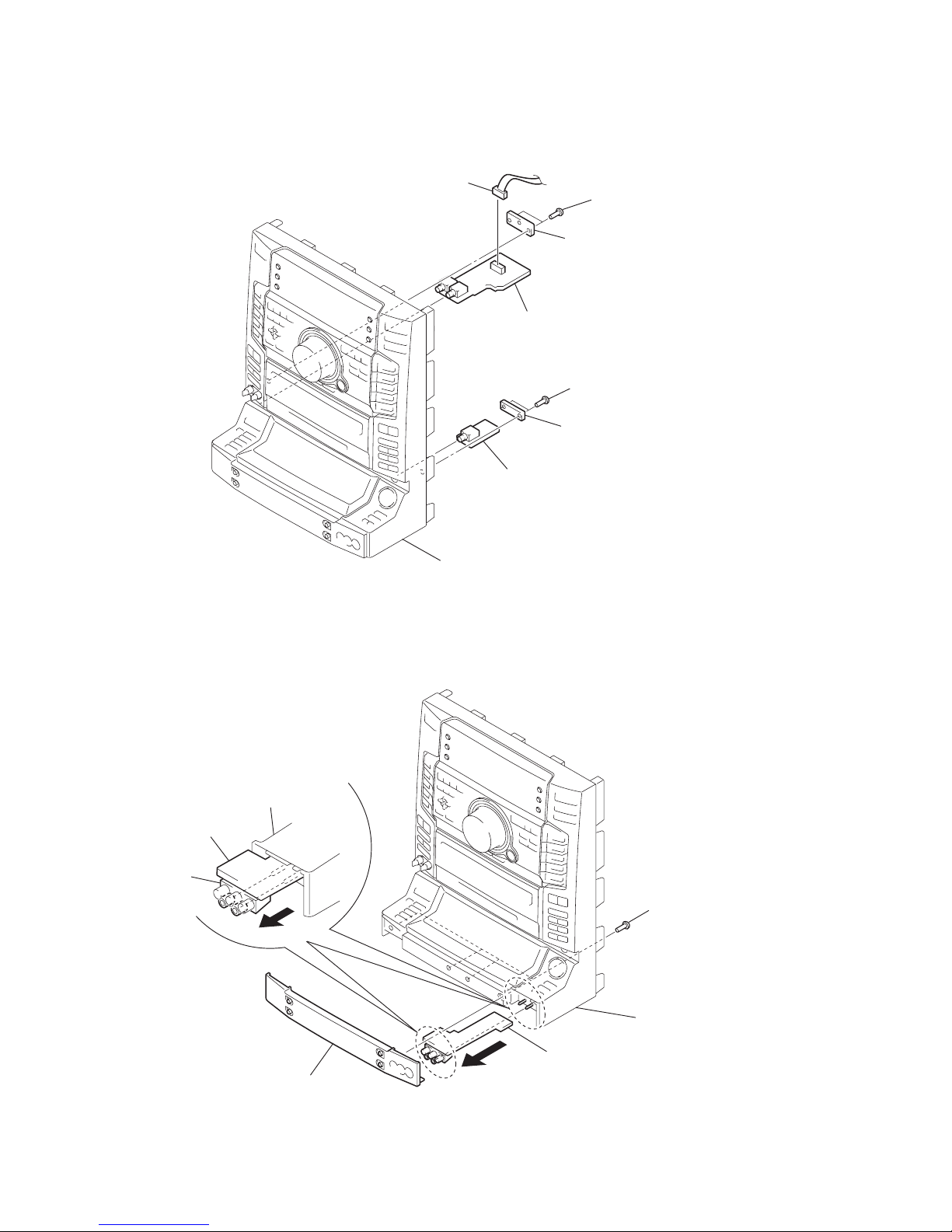
2. DISASSEMBY··································································· 7
3. TEST MODE···································································· 15
4. MECHANICAL ADJUSTMENTS ····························· 17
5. ELECTRICAL ADJUSTMENTS ······························· 17
6. DIAGRAMS
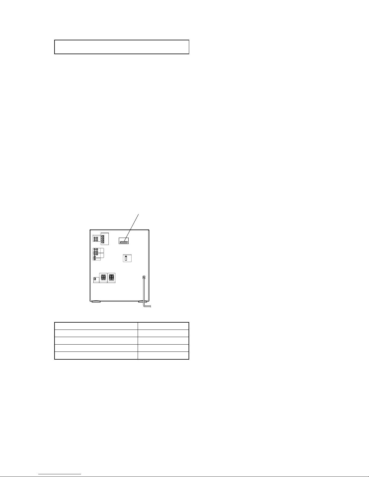
6-1. Circuit Board Location ······················································ 21
6-2. Block Diagram – CD Servo Section –······························· 22
Block Diagram – Tuner/Tape Deck Section – ··················· 23
Block Diagram – Main Section – ······································ 24
Block Diagram
– Display/Key Control/Power Supply Section –·········· 25
6-3. Printed Wiring Board – BD Section – ······························· 26
6-4. Schematic Diagram – BD Section – ·································· 27
6-5. Printed Wiring Board – Motor, LED Section – ················· 28
6-6. Schematic Diagram –Motor, LED Section – ····················· 28
6-7. Schematic Diagram – MIC/Guitar Section –····················· 29
6-8. Printed Wiring Board – MIC/Guitar Section – ·················· 29
6-9. Schematic Diagram – Main (1/3) Section – ······················ 30
6-10.Schematic Diagram – Main (2/3) Section – ······················ 31
6-11.Schematic Diagram – Main (3/3) Section – ······················ 32
6-12.Printed Wiring Board – Main Section – ····························· 33
6-13.Printed Wiring Board
– CD-L,CD-R,Headphone,Front Input,D-SW Section – ·· 34
6-14.Schematic Diagram
– CD-L,CD-R,Headphone,Front Input,D-SW Section – ·· 35
6-15.Printed Wiring Board – Panel VR Section – ······················ 36
6-16.Schematic Diagram – Panel VR Section – ························ 37
6-17.Printed Wiring Board – Panel FL,TC-A,TC-B Section – · 38
6-18.Schematic Diagram – Panel FL,TC-A,TC-B Section –····· 39
6-19.Printed Wiring Board – PA Section – ································ 40
6-20.Schematic Diagram – PA Section – ··································· 41
6-21. Printed Wiring Board – Sub Amp Section – ····················· 42
6-22.Schematic Diagram – Sub Amp Section –························· 43
6-23. Printed Wiring Board – Trans,Sub Trans Section – ·········· 44
6-24.Schematic Diagram – Trans,Sub Trans Section –·············· 44
6-25. IC Pin Function Description ············································· 46
6-26. IC Block Diagram ····························································· 51
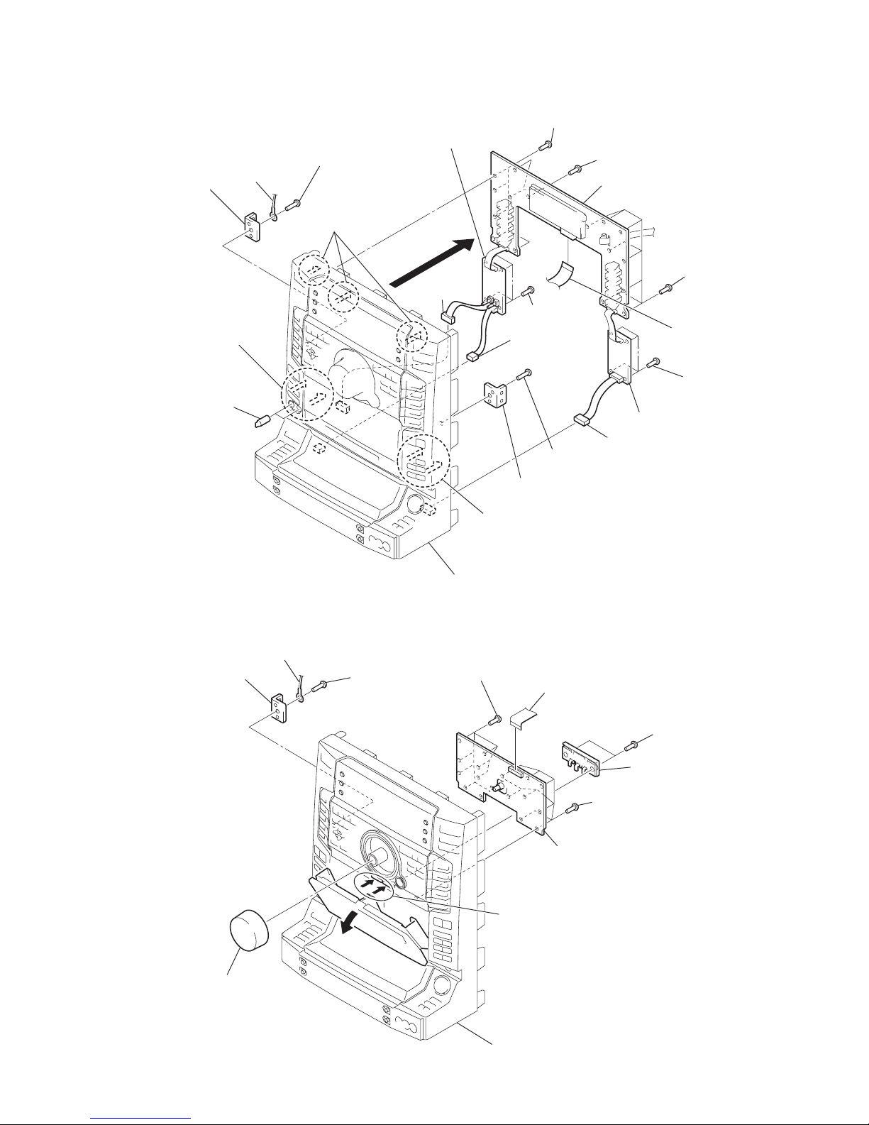
7. EXPLODED VIEWS
7-1. Case,Back Panel Section ···················································54
7-2. Front Panel Section-1 ························································ 55
7-3. Front Panel Section-2 ························································ 56
7-4. Chassis Section ·································································· 57
7-5. CD Mechanism Deck Section
(CDM-30BD60C)······························································· 58
7-6. Base Unit Section (BU-30BD60C)····································59
8. ELECTRICAL PARTS LIST ······································· 60