5
HCD-ZUX9
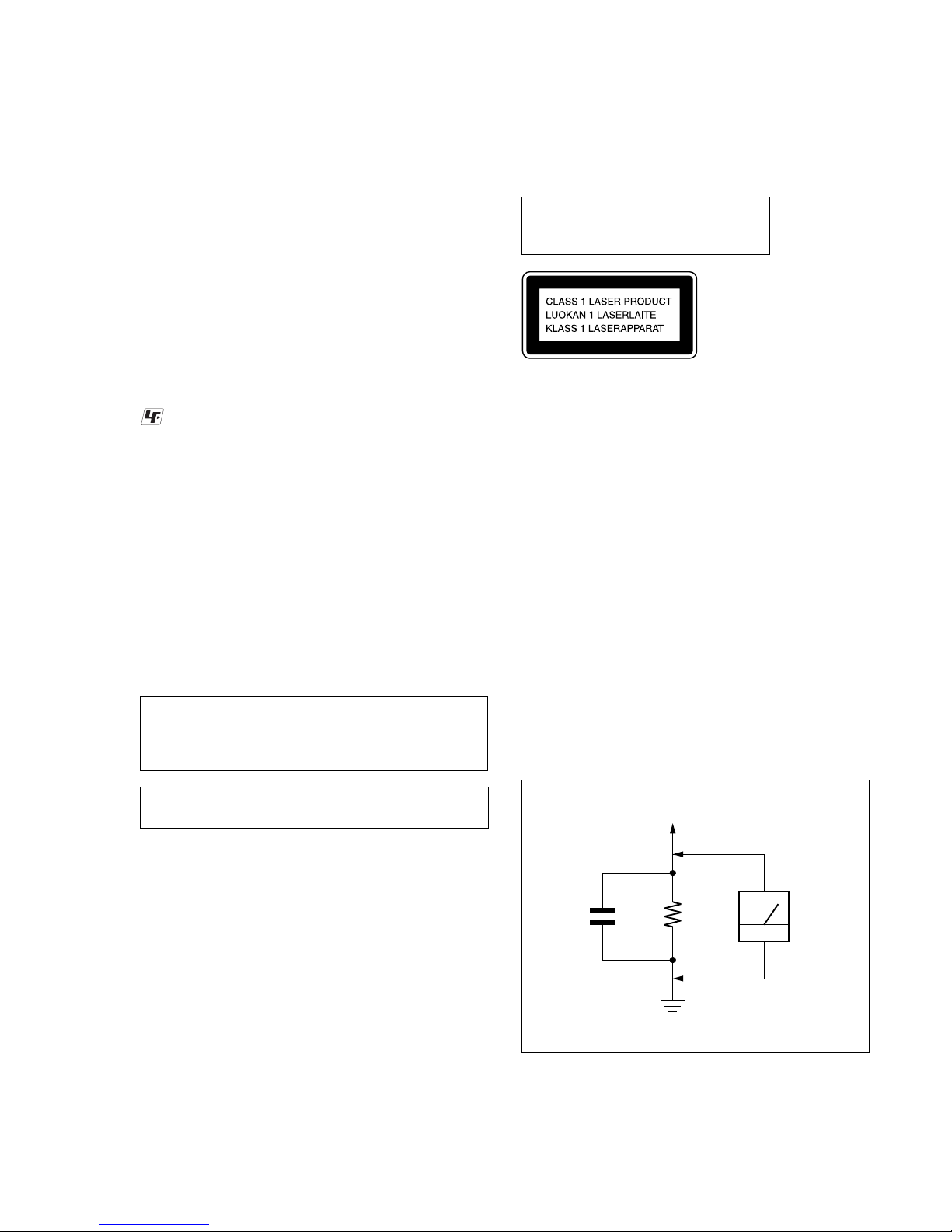
1. SERVICING NOTES
Loading Panel .................................................................. 6
2. GENERAL
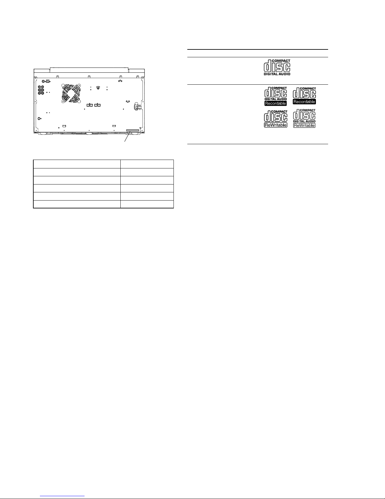
Guide to Parts and Controls............................................. 7
3. DISASSEMBLY
3-1. Side R Panel, Side L Panel .............................................. 16
3-2. Top Case Section ............................................................. 16
3-3. Back Panel Section .......................................................... 17
3-4. Loading Panel .................................................................. 17
3-5. Front Panel Section ......................................................... 18
3-6. Tape Mechanism Deck .................................................... 18
3-7. Holder (TC-L), Holder (TC-R) ....................................... 19
3-8. Power AMP Section ........................................................ 19
3-9. Main Board...................................................................... 20
3-10. FL Board, Power LED Board .......................................... 20
3-11. Illumination Board,VOL Board...................................... 21
3-12. MIC Board, Base R LED Board...................................... 21
3-13. HP-Video Board, USB Connector Board,
Base L LED Board .......................................................... 22
3-14. Center Key Board, Beat Creator Board,
X-Round Board ............................................................... 22
3-15. USB Board ...................................................................... 23
3-16. CD Mechanism ................................................................ 23
3-17. Driver Board, SW Board ................................................. 24
3-18. BD91 Board..................................................................... 24
3-19. Optical Pick-Up ............................................................... 25
3-20. Sensor Board ................................................................... 25
3-21. Motor (TB) Board ........................................................... 26
3-22. Motor (LD) Board ........................................................... 26
4. TEST MODE.............................................................. 27
5. MECHANICAL ADJUSTMENTS ....................... 31
6. ELECTRICAL ADJUSTMENTS ......................... 31
7. DIAGRAMS
7-1. Block Diagram – RF/Servo Section – ............................. 35
7-2. Block Diagram – Tape/Tuner Section – .......................... 36
7-3. Block Diagram – Main Section – .................................... 37
7-4. Block Diagram – Effector Section – ............................... 38
7-5. Block Diagram – USB Section –..................................... 39
TABLE OF CONTENTS
7-6. Block Diagram – AMP Section – .................................... 40
7-7. Block Diagram – Display/Power Section – ..................... 41
7-8. Printed Wiring Board – BD91 Section – ......................... 43
7-9. Schematic Diagram – BD91 Section –............................ 44
7-10. Printed Wiring Boards – Driver Section –....................... 45
7-11. Schematic Diagram – Driver Section – ........................... 46
7-12. Printed Wiring Board – Main Section – .......................... 47
7-13. Schematic Diagram – Main Section (1/4) – .................... 48
7-14. Schematic Diagram – Main Section (2/4) – .................... 49
7-15. Schematic Diagram – Main Section (3/4) – .................... 50
7-16. Schematic Diagram – Main Section (4/4) – .................... 51
7-17. Printed Wiring Boards
– HP-Video/MIC/USB Connector Section –................... 52
7-18. Schematic Diagram
– HP-Video/MIC/USB Connector Section –................... 53
7-19. Printed Wiring Board – USB Section –........................... 54
7-20. Schematic Diagram – USB Section –.............................. 55
7-21. Printed Wiring Board – Effector Section –...................... 56
7-22. Schematic Diagram – Effector Section – ........................ 57
7-23. Printed Wiring Board – PowerAMP Section – ............... 58
7-24. Schematic Diagram – Power AMP Section – .................. 59
7-25. Printed Wiring Board – FL Section – .............................. 60
7-26. Schematic Diagram – FL Section –................................. 61
7-27. Printed Wiring Boards – Key Section (1/2) –.................. 62
7-28. Printed Wiring Boards – Key Section (2/2) –.................. 63
7-29. Schematic Diagram – Key Section – ............................... 64
7-30. Printed Wiring Boards – LED Section (1/2) – ................ 65
7-31. Printed Wiring Boards – LED Section (2/2) – ................ 66
7-32. Schematic Diagram – LED Section –.............................. 67
7-33. Printed Wiring Boards – Power Section – ....................... 68
7-34. Schematic Diagram – Power Section – ........................... 69
8. EXPLODED VIEWS
8-1. Main Section.................................................................... 87
8-2. Front Panel Section (1).................................................... 88
8-3. Front Panel Section (2).................................................... 89
8-4. Front Panel Section (3).................................................... 90
8-5. Top Case Section ............................................................. 91
8-6. Back Panel Section .......................................................... 92
8-7. Chassis Section................................................................ 93
8-8. CD Mechanism Section (1) ............................................. 94
8-9. CD Mechanism Section (2) ............................................. 95
9. ELECTRICAL PARTS LIST................................ 96